downloadGroupGroupnoun_press release_995423_000000 copyGroupnoun_Feed_96767_000000Group 19noun_pictures_1817522_000000Member company iconResource item iconStore item iconGroup 19Group 19noun_Photo_2085192_000000 Copynoun_presentation_2096081_000000Group 19Group Copy 7noun_webinar_692730_000000Path
Skip to main content
Default Banner Image

semiconductors

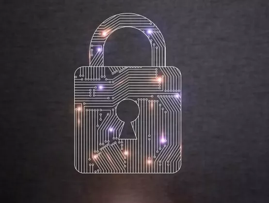
Even though microchips continue to get smarter, vital security gaps continue to be exposed through such hack attacks as Meltdown, Spectre, and in recent weeks, Plundervolt. Researchers continue to discover open doors in chip architectures for malicious players to steal increasingly sensitive data, hide the identity of counterfeits, or tamper with electronics systems most anywhere along the global microelectronics supply chain. Today, it’s impossible to have full visibility of the distributed chip making process – from design and fabrication to packaging, testing and delivery. That’s why our industry’s future hinges to a large degree on establishing a hardware root of trust throughout the silicon’s operational lifecycle. Trust but verify! It’s easy to say, but how do we do it?To gain insights, SEMI interviewed Dr. Mark Tehranipoor, currently the Intel Charles E. Young Preeminence Endowed Chair Professor in Cybersecurity at the University of Florida’s Electrical and Computer Engineering Department. A foremost authority on microelectronics security and trust, counterfeit electronics detection, and supply chain risk management, Dr. Tehranipoor will be a keynote speaker at the SEMICON Taiwan Security on Chip Summit, Friday, September 25, where a full program of industry leaders will address key security challenges and solutions involving IoT, systems on a chip (SoCs), integrated circuits, physical unclonable function (PUF) technology, future design, certifications, managed services, and more.For additional insights and to hear Dr. Tehranipoor’s full presentation, register for SEMICON Taiwan 2020, which SEMI is holding as a hybrid event with both a virtual format and an in-show program September 23-25.SEMI: What are the major uncertainties in providing the hardware root of trust within the cyber domain?Tehranipoor: One of the most critical issues we’re dealing with now is loss of control over the process of designing and fabricating integrated circuits and systems. This has happened along with globalization and the movement of supply chain operations overseas to lower costs of nearly all goods, including electronics products and semiconductors. As skill sets, talent, design and fabrication have all shifted offshore, concerns have also risen about security controls across the many different segments of the microelectronics supply chain.For example, when you think about the security of military, space, transportation, power grids, financial or other networks, it becomes a major concern if you cannot trust the underlying electronics system that runs them. New SoCs are also holding more sensitive data around encryption keys, biometrics, personal information or banking data. And as reports escalate about cybersecurity gaps at the electronics part level, it’s increasingly important to establish a hardware root of trust. Today, it’s not enough for a buyer to just call up the design house and verify the electronic ID of an asset. The ID might match, but the device could have been tampered with or replaced with a counterfeit somewhere along its end-to-end journey. Unlike software or networks where problems can be automatically identified, upgraded and fixed, verifying electronic hardware is a costly and time-consuming process, especially when they’re as complex as microchips. It can take months to deconstruct, reverse engineer, inspect, and authenticate a chip. By then, discovery of any security breaches is too late.When addressing the security of electronics systems, there are three important features to keep in mind. First, there’s confidentiality. The device shouldn’t leak information to an unauthorized user. Second, there’s integrity. Unauthorized users should not be able to manipulate an SoC’s sensitive data. The third feature is availability, which can be a result of Denial of Service (DoS) attacks. If the device is under attack and can’t access your online service or network, you must still have security measures for your electronics system to be available in a safe mode while you simultaneously identify the problem, recover from it, and return to normal functions.SEMI: What framework should be followed to establish greater trust and confidence across the entire microelectronics supply chain?Tehranipoor: In the United States, we recognize it may not be possible to bring all manufacturing, design, and delivery teams back to this country and have them certified by the U.S. Department of Defense. You could do some of it, but it would be very costly and complex to bring back all the design, fab, testing, and packaging operations involved with electronics systems and still have complete control.The most practical approach is to make sure we design electronic systems with security and trust in mind from the start. We need to provide security features up front throughout the extended supply chain – into the design flow, fab flow, and out into the field to make it easier and faster for anyone at any point to verify the authenticity of an electronic system as well as identify and mitigate a problem. Finally, we have to remember that we are all in this together – designers, developers, packaging facilities and fabs. We can’t just blame semiconductor manufacturers or any other single entity. As a result, we must be cooperative and collaborative by focusing on this issue as a consortium. Everyone in this ecosystem must come to the table, share best practices, establish standards, and initiate best practices for device to system authentication.SEMI: How can SEMI and the SEMI Electronic System Design (ESD) Alliance help the industry meet these challenges?Tehranipoor: It’s certainly of utmost importance for members of organizations like SEMI and its ESD Alliance committees to jointly develop and adhere to standards or guidelines that establish hardware root of trust across all participants in the global supply chain. At the same time, such alliances should make it a high priority to protect each company’s intellectual property (IP). Collectively, we need resolutions that allow us to develop unique IPs and more easily trace, identify, and verify the authenticity of electronics systems as they flow throughout the end-to-end electronic supply chain. Great efforts are under way and progress is being made. But it’s not enough. Clearly, more needs to be done to establish root of trust standards at the chip level.I can’t emphasize enough the importance of consortia like the SEMI ESD Alliance to create an environment where industry, government, and academia can come together, share best practices and even case studies on how they handled security vulnerabilities and breaches. We understand that not everyone wants to share their security problems, vulnerabilities, or attack surfaces, but learning from each other’s experiences can have a tremendous impact on industrywide progress. If you don’t know what you need to address, you won’t be able to address it when it happens.I also encourage organizations like SEMI to create standards or guidelines that reduce the complexity of microchip designs for security purposes. Realtors often say there are three things to consider in finding a home that will appreciate in value: Location, location, location. To build more secure electronics systems, my mantra is: Automation, automation, automation. Complexity is the enemy of security. By using automation to simplify security mechanisms and detect inconsistencies, it will be easier to find and fix security problems, not to mention lower costs at the same time. SEMI: What will an attendee take away from your talk at SEMICON Taiwan?Tehranipoor: I have a large team of researchers who day and night spot vulnerabilities by attacking and assessing data from different electronic systems set up in our labs. Attendees will see real-world examples and lab animations that show how electronics systems can be hacked most anywhere across the supply chain. They will also learn about step-by-step security solutions we have developed at the microchip level. We need to do a better job of protecting the security of our semiconductor assets and the electronic solutions or services they power. My call to action will be that we need to invest more in research and foster an environment of more open trust and cooperation. We can do this by bringing together different countries, companies, and organizations in the microelectronics ecosystem to overcome this major challenge.Dr. Mark Tehranipoor is currently the Intel Charles E. Young Preeminence Endowed Chair Professor in Cybersecurity at the ECE Department, University of Florida. He is currently serving as Director for Florida Institute for Cybersecurity Research (FICS), National Microelectronics Security Training Center (MEST), CYAN Center of Excellence, and ECI Transition Center. He also serves as Program Director of Cybersecurity for UF Herbert Wertheim College of Engineering. His current research interests include IoT security, hardware security and trust, and reliable circuit design.Samer Bahou is senior manager of corporate communications at SEMI.
Read More
Teck Khiong, WOI, senior manager of Factory Integration at Infineon Technologies Asia Pacific Pte Ltd, recently shared with me how the Infineon backend plant in Singapore has benefited from its journey to qualify for the lighthouse certification.WOI is driving Infinion smart manufacturing projects with a strong focus in the area of connect and control using IoT (Internet of Things) and analytics technologies. Ng: How did the Infineon backend plant in Singapore distinguish itself to qualify for lighthouse certification? WOI: The Infineon Singapore backend manufacturing plant is proud to be a Lighthouse Certified Smart Manufacturing site as part of the World Economic Forum’s (WEF) Fourth Industrial Revolution platform. Our Industry 4.0 (I4.0) implementation reduces labor costs by 30% and improves capital efficiency by 15%. We drove this successful digital transformation continuously investing in our people development and digital backbone.Of the many initiatives under our I4.0 Smart Factory platform, five were selected for WEF Lighthouse submission and certification. Digital foundation with integrated connectivity and workflow execution We implemented an Internet of Things (IoT) framework to connect machines to manufacturing system more than two years ago. The digitization of our Work-in-Progress (WIP) management systems provides full traceability and gives us better control of the four Ms (Man-Machine-Method-Material). Material handling and process automation We progressively deployed automated solutions starting six years ago using autonomous transport, robotic material management systems and automation of packing processes. This eliminated non-value touches in areas of WIP storage and retrieval. Advanced algorithms enabled WIP scheduling and dispatching As our product mix and volume grew in complexity, our advanced algorithms has enabled us to increase our machine uptime, thus reducing idle and set-up time. Manufacturing control tower Our control tower provides a real-time pulse of the entire manufacturing process, from machine efficiency to quality. The tower also improves data integrity and collaborative information sharing while issuing early-warning alerts that enable exception management and timely decisions. Running a global virtual factory Our Global Production Network deployments allows us to connect and manage a growing contract-manufacturing network in real time, with the same transparency, traceability and control as if the manufacturers are our internal sites.About Teck Khiong, WOITeck Khiong, WOI graduated from Loughborough University in the UK with a Master of Science degree in Computer Integrated Manufacturing (CIM). For more than 20 years he has delivered manufacturing IT solutions to global backend (assembly and test) semiconductor manufacturing, ranging from equipment, factory, process control, material handling automation and manufacturing execution systems (MES).
Read More
Is your company working on the next big thing in flexible, hybrid and printed electronics – a breakthrough or innovation that will make the world safer, healthier or more productive for years to come? If so, we want to hear from you.You’re invited to deliver a technical presentation at virtual FLEX 2021, February 22-26, 2021. The call for abstracts is now open! Celebrating its 20th year, the online event will gather executives, product managers, business development professionals, and engineering directors as well as leading industry analysts and media for the latest developments, trends and innovations in flexible hybrid electronics (FHE). More than 400 companies, universities, R D labs, and government agencies from around the world have participated in FLEX conferences.Technical presentations should focus on the conference theme, 20 Years of Driving Innovation to Make the World Safer, covering flexible hybrid or printed electronics products, equipment, processes, materials, and the applications they enable. FLEX 2021 also takes aim at the future of the planet, so presentations on global sustainability in areas such as impacts, strategies, tactics, successes and progress area also a great fit. To submit your abstract, please complete the online form: Upload your abstract (100-300 words) describing the topic of your presentation and how it applies to the flexible, hybrid, and printed electronics products. Preference is given to original research and advancements in process and materials as they relate to end users. We also invite students from research universities to submit posters describing their work and results for the popular FLEX Poster Competition. As in the past, a panel of industry and academic experts will evaluate the posters and recognize the top three students and their work. Here are key deadlines and dates for industry experts and students to keep in mind: September 30, 2020 – Submit your abstract. October 31, 2020 – We’ll notify you whether your presentation has been accepted by this date. November 15, 2020 – Sign a Speaker Agreement and provide a bio and headshot. February 1, 2021 – Send us an electronic copy of your presentation. We’re looking for presentations in these topic areas: Flexible Hybrid Electronics Systems Materials Processing Sustainability and Power MEMS and Sensors Applications Presentations should include the following: Why the technology presented matters and to whom Practical recommendations for addressing commercialization issues or applications. This includes providing innovative technological or market solutions driven by a use case, the integration challenges you faced, and the system-level architecture decisions you made. Descriptions of how you overcame each challenge Ideas for what as an industry we should be working on and what are you working on to demonstrate sustainability For a full rundown on topics and other information, please visit the FLEX 2021 Call for Papers web page.Michelle Fabiano is a program and event manager for SEMI Americas.
Read More
MEMS and image sensors are shining stars in the chip industry as technology companies worldwide accelerate innovation in the fight against COVID-19. The tiny devices are behind advances in areas of electronics ranging from thermal imaging and faster point-of-care testing to microfluidics-based polymerase chain reaction (PCR) tools and techniques to detect SARS-CoV-2.SEMI recently spoke with Yole Développement analysts Dimitrios Damianos and Chenmeijing Liang about MEMS and imaging sensors market trends and how microelectronics-enhanced technologies are supporting the worldwide push to contain the spread of COVID-19.For additional insights on the technologies, join the SEMI MEMS Imaging Sensors Summit, held for the first time at SEMICON Europa, 12-13 November 2020 in Munich, Germany. Registration is open.SEMI: Despite the global pandemic, the MEMS and sensors market is still growing and is one of the healthiest industries, not only in Europe, but globally. What is driving this growth?Damianos: MEMS have been continuously evolving from the first sensors that were measuring pressure and acceleration to rotation sensing and visible light management followed by light sensing beyond visible and the expansion to ultrasound and multi-spectral. Now we are heading towards an era where we want to sense every aspect of our environment, with more processing and eventually analytics bringing more quality to the data.COVID-19 has impacted various global markets in very different ways. While automotive, mobility and civil aviation have suffered, the impact on telecommunications and medical has been positive. The effects on the consumer, mobile and industrial markets have been moderate. Moreover, COVID-19 is changing the perception of the current global supply chain in manufacturing, potentially leading to more localized value chains and further regionalization in order to minimize similar risks posed by the pandemic and the first lockdown.SEMI: Who are the main MEMS players based on your research? Damianos: For MEMS players, the picture in 2019 was not the same as 10 years ago, when Texas Instruments (TI) and Hewlett-Packard (HP) were leading the scene, with Bosch and ST Microelectronics following, all at comparable revenue levels. Now, Broadcom and Bosch lead with almost $1.4 billion in revenue each, and the rest of the MEMS key stakeholders compete in the $400 million to $600 million league. Microphone players profited from the voice interface adoption trend, while players active in MEMS for mobility and smartphones suffered slightly due to weak end-system demand.SEMI: What scenarios can we expect for each market with regard to the impact of COVID-19 on MEMS for 2020? Damianos: For 2020, at Yole Développement we expect the consumer market to contract slightly by 2.6%, with the automotive market to dip by 27.5%, and defense and aerospace by 20.5%. For the defense market, no major effect is expected, as all major programs still run for the year. The market may experience some slight delays in deliveries due to supply chain and logistics problems. However, sensors integrated in commercial/civil aerospace applications will suffer due to the general paralysis of the air travel industry. On the positive side, telecommunications could increase by 4.7%, medical applications by 10.6%, and industrial by 11.5%.Due to the global pandemic, some types of MEMS have spiked in demand this year. For example, demand for thermopiles and microbolometers used in temperature guns and thermal cameras has increased because of the need for contactless monitoring of people’s temperatures. Moreover, microfluidics for DNA sequencing and real-time polymerase chain reaction (PCR) diagnostic tests for detecting COVID-19 are gaining market relevance, with the latter serving as a premier method of detecting a bacteria or virus on the molecular level with high degrees of accuracy. Furthermore, pressure and flowmeters in ventilators will grow because of huge demand by hospital intensive care units (ICUs).SEMI: What growth trends do you predict for the long haul?Damianos: In the longer term, we expect global MEMS volumes to almost double, from 24.4 billion units in 2019 to 50.8 billion units in 2025, with a 13% CAGR during the same period. The global MEMS market could reach $17.7 billion in revenue by 2025.We see a trend to more wearable devices integrating a lot of sensors but also a move to a more consumer-oriented healthcare. Moreover, everything related to voice interfaces and voice/virtual-personal assistants (VPAs) will continue to see strong growth, increasing demand for MEMS mics with better quality and high-fidelity voice capture. MEMS devices are shifting to higher accuracy, ultra-low power, embedded intelligence and possibly some bio-compatibility for medical applications.MEMS players will try to escape the commoditization cycle and deliver more value by increasing the value of the data, either grouping many sensors to create sensor hubs or by adding processing, algorithms and software. Industry players are employing strategies such as adding extra processing close to the sensor (e.g. Knowles) or ameliorating the use cases of their applications of their clients (e.g. Bosch or ST). AI on the edge seems very alluring for extra value acquisition, with many startups already working on it. Some examples include always-on-sensing (Aspinity in collaboration with Infineon, Syntiant), echolocation (IMERAI) and predictive maintenance using inertial sensors (Cartesiam). This will be the next pit stop for MEMS technology for sure. SEMI: The CMOS Image Sensor (CIS) is a cornerstone technology in the development of devices powered by machine sensing and artificial intelligence (AI) for applications such as advanced driver assistance system (ADAS). CIS powers many of the ongoing revolutions in new technical products and use cases. What is the status of the image sensors industry? Liang: Last year was exceptional with a combination of high demand and high prices due to capacity limitations. Q4 2019 went way above the forecast, and, in the end, the CIS industry reached $19.3 billion for the full year. This year, we think it will return to normal, and, despite the pandemic impact, we expect significant growth in the range of 7% to 12%. Last year’s 25% year-over-year (YOY) growth was the highest we’ve seen over the past decade. Mobile still dominates the marketplace for CIS with 69% market share. Two markets, computing (8%) and consumer (5%), are adjacent to the mobile market but progressively losing ground due to the smartphone disruption.Security, at 6% market share, will probably be the second largest CIS market in the future. Although this is an area of excellence for the emerging Chinese players, unfortunately, they could be hit by the current trade war. The automotive market did very well from 2018 to 2019 because of the numerous applications recently developed for ADAS, viewing, and in-cabin applications. Lastly, the industrial camera applications benefited from large investments in automation, especially in the semiconductor and automotive industries, but here again many uncertainties remain as these markets will reshuffle in the post COVID-19 world. SEMI: Which CIS markets are most susceptible to seasonality and the impact of COVID-19?Liang: According to our quarterly CIS monitor, automotive and security were both negatively impacted by the pandemic beyond what we expected in terms of seasonality. For computing, the situation improved just prior the lockdown. Q1 got a positive impact with high sales results for laptops and tablets, but no significant impact was seen for security equipment. For automotive, the demand for cameras was very high in Q1, which is seasonally normal, despite the decrease of car shipments that followed later. The automotive CIS market in 2020 should remain relatively flat compared to 2019 due to the higher attachment rates of cameras despite the lower number of cars produced. Consumer and industrial segments dropped in Q1, which is typical early in the year.The next five years might be a bit slow, and although we forecast growth for the next year, in the future the market share will be lower in mobile. In fact, mobile CIS growth will fall below the CIS growth average, but we will see an increase of market share for the security, automotive and industrial segments. The CIS market could reach $28 billion in 2025.At first, COVID-19 had a limited impact on the production side, as factories in China are usually closed for the New Year holiday, when the pandemic started. While supply is currently recovering, we still consider the limited impact on demand. Smartphone production for 2020 will be down 6%, but camera shipments for mobile should increase about 10% this year. Another positive trend for the mobile market is optical fingerprint implementation. Currently, high-end Android phones use this kind of technology. For 2023, we estimate optical fingerprint technology revenue to be over $1 billion.The roadmap for the automotive market is driven by camera proliferation. We’ll see 10 cameras per car and more for some high-end vehicles. Increasing demand for safety and convenience will mean more cameras per car in the future. With a strong attachment rate, the market average in automotive is around 2.0 cameras per car nowadays, and we expect the market average to reach 3.5 cameras per car in 2025. In security, Charge Coupled Device (CCD)-based cameras are nearly out of the market, as CMOS-based IP cameras are most important now.SEMI: What are current key technology trends?Liang: 3D semiconductor technology is the hot topic. CIS wafer staking technology is indeed at the center of the CIS technology race. Future applications could be AI analytics or recently developed applications on new types of CIS. So far, we have seen the introduction of variants of the CIS pixel. Global shutter (GS) and indirect Time of Flight (iToF) were recently introduced, and now direct time-of-flight (dTOF) pixels are being used in high volume. 3D semiconductor technology is a bonanza for the industry, as it allows to pack more value in a single chip. While the surface of silicon is still increasing, additional silicon is added through stacking.With COVID-19 still a problem, the endpoint for smartphones in 2020 remains uncertain. The short-term impact for CIS will be slower growth with respect to the 25% YoY of last year. The downturn in car production will be mitigated by an increased attachment rate for automotive cameras. The security market will also help maintain CIS growth.For more insights, see the following reports: Status of the MEMS Industry 2020 3D Imaging and Sensing 2020 CIS Market Monitor Q2 2020 Dimitrios Damianos is a technology and market analysts at Yole Développement covering MEMS, Sensors, Photonics and Imaging. Chenmeijing Liang is a technology and market analysts at Yole Développement covering Imaging. Serena Brischetto is senior manager of Marketing and Communications at SEMI Europe.
Read More
To attract and cultivate new talent across the microelectronics industry, virtual SEMICON West 2020 offered wide-ranging career insights for engineering students seeking that vital first job and young employees embarking on their careers. They learned about overcoming challenges at work and gained a competitive edge by connecting with industry leaders for insider knowledge. These are just some examples of how the SEMI Foundation and the SEMI Workforce Development and Diversity, Equity and Inclusion (DEI) initiatives serve as a springboard to careers in the industry and help close its talent gap.Following are experiences of aspiring engineers at SEMICON West and career lessons presented to help them shape the future of our semiconductor industry.Jump-Starting Careers at SEMICON West 2020More than 600 students from over 50 colleges and universities across the Unites States joined SEMICON West 2020 to jump-start their careers in the semiconductor industry. With free access to SEMI’s first virtual expo, they connected with recruiters and companies in the exhibit hall, and sponged up insights from speakers about digital internships, job opportunities, and key trends shaping the digital future.“It was almost overwhelming,” said Jason Wong, 20, a junior at San Jose State University working toward an advanced degree in mechanical engineering. “It was kind of like an engineering student’s dream for contacts and knowledge all on one platform.”Wong visited about 15 booths in the online exhibit hall to speak with company representatives about his field of interest – microelectromechanical systems (MEMS).“MEMS is a pretty niche area, so it was really surprising how many companies were there in this category alone,” Wong said.Through the expo’s chat tool, Wong made some solid contacts and has followed up with several engineers via email, LinkedIn and Zoom meetings, cultivating what he believes will be “some long-lasting and valuable connections.”“I’m not really looking for a job at the moment, but I hope to get an internship at some point,” Wong said. “With the current (COVID-19) outbreak, a lot of events with opportunities to interact are no longer available, so this was an enlightening and useful experience for me I plan to attend again.”On the other side of the country in Virginia, Devayani Pawar, 23, found it easy to network at SEMICON West. She especially appreciated the free pass for students and practical sessions in the Smart Workforce Pavilion tailored to help early-career job seekers find opportunities, build contacts, and polish resumes.She was drawn to the Smart Manufacturing Pavilion because of her skills and interests in toolmaking and wafers.“I understand manufacturing and it’s a hot field right now,” said Pawar, who recently earned her master’s degree in data science from George Mason University. “It’s interesting to me how such tiny components can do so much powerful work.”“A lot of people my age aren’t very aware of the microchip industry – they’re mostly focused on information technology and companies like Google, Amazon, or Facebook,” Pawar said.After landing an internship at Micron Technology analyzing wafers and working in clean rooms, she was wowed by the potential of nanotechnology. Pawar learned about the strong demand for data scientists in semiconductor manufacturing. After making connections at SEMICON West and absorbing information, she now has a better handle on career opportunities.“The recruiters and other contacts I made have been so responsive, and now I have a better understanding of use cases and what companies are seeking,” she said.A Day in the Life of an EngineerRight after college in 2017, Erika Gabrielle Hansen joined Applied Materials as an engineer. She told management she wanted to travel, learn about the “big picture” behind the company’s products, and work with customers.In her presentation A Day in the Life of an Engineer at the SEMICON West Smart Workforce Pavilion, she recalled a whirlwind of unforeseen opportunities, soul-searching challenges, and the rewards of personal, professional, and community growth. She also candidly shared lessons learned about pride, collaboration, and resilience.Her journey began when she had the opportunity to share her aspirations for her at career at Applied and landed a dual role as a process engineer and customer account technologist.In her job as a process engineer, Hansen puts her materials engineering degree from Cal Poly, San Luis Obispo to good use analyzing data, solving technical problems, developing new processes to meet customer requirements, and working with cutting-edge technologies. At one moment she might be in a clean-room laboratory wearing a bunny suit doing hands-on work with tools. In another, she could be videoconferencing with hardware, software, and systems engineers worldwide, or preparing a report for upper management.“I was very nervous at first as a process engineer,” Hansen said. “I was the only person in my group who didn’t have a Ph.D. and tried to compensate for that by doing things on my own and not asking for help.”After making a few mistakes, she began to turn to her team for their expertise and sharing the results of her work – both good and bad – with them.“Having humility to ask for help and not let pride get in the way was a huge learning point for me,” she said.As a customer account technologist, she has made a dozen trips to customer sites in four countries to implement new processes or resolve technical issues. By seeing tools in action, she now has what she calls a “whole picture” perspective on their effectiveness, while enjoying the camaraderie of colleagues and sampling local cuisines, sites, and scenes around the world.At one point, she was assigned to lead an international team to resolve an issue with a major customer – her greatest challenge yet and her first time in such a role. She struggled to overcome language barriers and eventually told her boss she might not be the best person to lead the project. He promised to provide more support, and her team went on to resolve the customer’s problem.“I picked myself up, reached out to people with international experience, and changed my communication style,” Hansen said. “I learned it’s okay to be uncomfortable, to flex my leadership style, and be resilient, which is a learned skill.”Building a Better Network: Crucial ConnectionsAndrew Carnegie, one of history’s richest industrialists and most generous philanthropists, said 85 percent of a person’s success is based on “interpersonal relationships” and “abilities to be a human being.” Professional skills account for just 15 percent of success.While advancing to her current role as Chief Marketing Officer for FormFactor, Amy Leong found this advice critical to her career trajectory. Just like the challenge of raising a strong family, building a successful career “takes a village… you can’t do it alone,” she said in her Smart Workforce Pavilion presentation Building a Better Network: Crucial Connections.Outperforming expectations might be essential early in one’s career to get promotions, raises, and the attention, but that mindset goes only so far.“As seniority levels increase, people already know you’re a phenomenal performer and expect nothing less,” Leong said. “So, the higher you go the more vital it is to spend almost a disproportionate amount of effort on building relationships.”Building your network isn’t about the quantity of one’s business cards or LinkedIn connections; it’s about building quality relationships with mutual benefits over the long run.“We need to be smart about return on investment when building our professional network,” she said. “You help me, and I help you. It’s win-win horse trading.”And the most important factor in career success? For Leong, a strong family foundation has mattered most.“Family comes first,” said Leong, who has twin teenagers. “Take care of the ones you love. Check in with your family whenever you can. Family relationships are bound by blood. Thanks to my retired parents and a helpful husband, we tough it through.”She reemphasized the importance of mutually beneficial relationships, noting “A rising tide will lift all boats.”Fostering Talent for the Industry’s FutureDeveloping young talent and future leaders in microelectronics stands as a persistent and growing need – and a critical challenge to realizing expected growth. Emerging technologies such as artificial intelligence, quantum computing, and augmented/virtual reality are expected to impact a huge range of markets, leading to projections that the semiconductor industry will double in size in the next 10 to 15 years.The opportunities for growth and technologies that promise to improve the quality of human life worldwide are breathtaking. The industry’s talent pool will need to scale accordingly, magnifying the importance of expanding industry-wide programs such as the Workforce Development and DEI initiatives that the SEMI Foundation are building. Learn more about how you and your company can get involved with these initiatives on the SEMI Foundation website.Shari Liss is executive director of the SEMI Foundation. She oversees SEMI Workforce Development programs from K-12 through re-skilling for veterans.
Read More
SEMI Korea is back on track. New confirmed COVID-19 cases in Korea now average about 50 per day – with more than half from abroad – after peaking in early March, setting the stage for the Seoul office’s first on-site program since the global coronavirus outbreak began.For four days in late July, SEMI Korea held the Semiconductor Process Technology Tutorial (SPT Tutorial) at COEX, home to SEMICON Korea. Nearly 180 university students and chip engineers gathered for two semiconductor manufacturing courses (beginner and intermediate) taught by professors from schools including Hongik and Sungkyunkwan Universities and senior engineers from major semiconductor makers. The beginner’s course covered the end-to-end chipmaking process and the intermediate class examined key phases of semiconductor manufacturing including silicon wafer preparation, cleaning and CMP, lithography, etch, metrology and inspection, implantation and diffusion, deposition and packaging.Social distancing, now part of daily life in Korea, and other protective measures implemented by SEMI Korea to ensure the safety and well-being of the attendees and lecturers made the event possible. SEMI Korea followed best COVID-19 practices including the following.Step 1. Site check of COVID-19 prevention systemCOEX is amply equipped with sanitizers and thermal imaging cameras, with medical staff available in case of an emergency. COEX also constantly monitors air quality at the entire facility while keeping it well-ventilated. Step 2. Screening of registrants Online medical questionnaire review: After attendees completed a SEMI Korea medical questionnaire and submitted it prior to registration, SEMI Korea checked the health status of each attendee and whether they had recently traveled overseas to a high-risk COVID-19 region. Registrant identification: Upon each registrant’s arrival at COEX, SEMI Korea confirmed that the identification of each attendees matched the registrant who completed the questionnaire. Temperature measurement and sanitizer use: SEMI Korea required all attendees to apply hand sanitizer before entering the classroom and measured the body temperature of each. Anyone running a temperature would have been denied entry. Mask Wearing: All attendees were required to wear mask socially distance during check-in and the lectures. Attendees line up for registration while social distancing. Step 3. Badge Distribution and Classroom Entry: Once attendees had passed through all the safety protocols, they were given badges and admitted to the lecture room. Each classroom table was equipped with acrylic desktop social distancing shields to contain the respiratory aerosols of the students. In addition, only one-way passage was allowed through entrances and exits to minimize contact among participants. Acrylic desktop shields helped with social distancing. "Thanks to SEMI's thorough COVID-19 prevention plan for COVID-19, both the speakers and attendees participated in the tutorial confident that the environment was safe,” said speaker Professor Taesung Kim of Sungkyunkwan University. “I look forward to seeing SEMI continue to take these precautions to help the semiconductor industry remain connected and grow.”SEMI Korea moves forward with nine on-site events in 2020Webinars will continue to serve as important forums for SEMI Korea to help members connect, collaborate and innovate while preventing the spread of COVID-19. But to help the industry grow and prosper, SEMI Korea’s on-site events – which have always and will continue to make safety the top priority – will remain robust.In 2020, SEMI Korea will host nine on-site events including the MEMS Sensor Forum and SMC Korea. We appreciate the industry’s support and cooperation as the world continues to battle COVID-19 and look forward to connecting with members in webinars and at on-site events again soon!Jaegwan Shim is a marketing specialist at SEMI Korea.
Read More
I recently spoke with Andrew Goh, Vice President at General Manager at Lam Research Southeast Asia, about the importance of the company's new production facility in Penang and its COVID-19 relief efforts. Ng: Before we delve into details, please provide a quick introduction to Lam Research Southeast Asia for our readers who aren't as familiar with your work. Goh: As you know, Lam Research is a leading supplier of wafer fabrication equipment and services to the global semiconductor industry. Since we were established in 1980, Lam has played a key role in contributing to the extraordinary pace of innovation in the semiconductor industry. We have always developed innovative solutions that help our customers build smaller, faster, more powerful, and more power-efficient electronic devices – the kind that are driving the proliferation of technology in our everyday lives.Further to this, we established Lam Research Southeast Asia in 1992 to better serve our customers in this region. We have about 260 employees in both Malaysia and Singapore, with more than two-thirds of them in engineering or technical roles.Ng: Early this year, Lam Research announced a new advanced technology production facility in Malaysia. Please tell us about it.Goh: Yes, Lam Research and the Malaysian Investment Development Authority jointly announced in February 2020 that Lam selected Batu Kawan Industrial Park in Penang, Malaysia as the location for a new advanced technology production facility.Our new state-of-the-art manufacturing site in Penang’s Batu Kawan will open in May 2021 and be the largest in our network. The current plan envisions a 700,000 square-foot facility with expansions already anticipated to serve current and future customers. Construction started in May 2020, and we aim to have our first shipment by 2021. We are currently at our temporary site in Bayan Lepas.Ng: As Lam’s manufacturing site, what role does it play in the larger organisation?Goh: The semiconductor industry is expanding and so are we. To help our customers move the world forward, we need a dynamic, energized team with initiative and focus to help establish our footprint in Malaysia. This has led to the expansion of our existing global production footprint with locations in the United States, South Korea, and Austria. As the industry moves forward, we at Lam Manufacturing Malaysia will work on the entire portfolio of our leading-edge products, collaborating closely with customers to create some of the world’s most sophisticated processes and fabrication equipment. We chose Penang for its talented workforce with experience in aerospace, health sciences manufacturing and other high-tech fields. We are currently hiring now for our site in Penang. Anyone interested in exploring job opportunities at the site can send learn more and apply at www.MakeAtLamPenang.com. Artist's rendering of new Lam Research production facility at the Batu Kawan Industrial Park in Penang. Ng: With the world now thrown into an unprecedented situation, do you expect any delay in the construction schedule?Goh: Despite the COVID-19 pandemic, construction began in May 2020. We still expect to make our first shipment from the Batu Kawan factory around mid 2021, in line with our initial estimates. Close cooperation with and timely support from MIDA and Invest Penang have allowed us to stay on track.Ng: How has Lam done supported COVID-19 relief or recovery efforts during this pandemic?Goh: Just as with any other business, this pandemic indeed is a trying time for all of us around the world. We announced on April 8 that we are donating $25 million to global COVID-19 relief and recovery efforts, which includes relief funds to employees, employee benefit resources, and additional support for the areas in which we operate. This support includes supplies for hospitals, both short-term and long-term community assistance, and our 2-for-1 gift matching for eligible COVID-19 relief programmes.In addition to the fund, we have also donated our surplus inventory of masks for immediate relief to local hospitals. At the same time, our innovative engineers and others with 3D printers at home have begun developing prototypes and printing protective face shields.Consistent with current guidance from the U.S. as well as the region’s respective Centers for Disease Control (CDC) and World Health Organization (WHO), we have activated our business continuity plan (BCP) to safeguard the health and well-being of our employees and their families, as well as to mitigate business disruptions to our customers. Measures we've implemented include strict social distancing, quarantine measures and travel restrictions.Bee Bee Ng is president of SEMI Southeast Asia.
Read More