
Gütenbach, Germany – December 16, 2025 – RENA Technologies is proud to be a key industrial partner in a new 1.3 million Euro Government-funded project led by the National Physical Laboratory (NPL) and supported by the Department for Science, Innovation and Technology (DSIT). The initiative will establish critical new metrology capabilities to strengthen the UK’s semiconductor innovation infrastructure and accelerate the development and adoption of next-generation semiconductor materials and processes.
This strategic investment underlines the UK’s commitment to maintaining global competitiveness in semiconductors, helping to attract private investment, strengthen supply chains, and support long-term economic growth. As advanced semiconductor materials become central to technologies such as electric vehicles, renewable energy, 5G communications and advanced electronics, robust measurement, verification and standards are increasingly essential.
The project brings together a broad consortium spanning industry and academia. Together, the partners cover the full innovation landscape, from materials research and process development to device fabrication and performance verification.
“At RENA, we develop advanced wet processing and surface treatment solutions that are critical in manufacturing of compound semiconductors and emerging materials. Through this collaboration, RENA will contribute industrial insight and process expertise to ensure that new measurement and testing capabilities are closely aligned with real manufacturing challenges.” States Peter Schneidewind, CEO of RENA Technologies.
While silicon remains the foundation of much of today’s semiconductor industry, many high-growth applications increasingly depend on advanced materials such as gallium arsenide (GaAs), gallium nitride (GaN), silicon carbide (SiC), and indium phosphide (InP). These materials offer superior performance in high-power, high-frequency and optoelectronic applications, but they also introduce new complexities in processing, characterization and quality assurance. Reliable standards and independent measurement methods are therefore essential to derisk innovation and support scale-up.
Through this project, consortium partners will work with NPL to:
• Develop new UK measurement and test capabilities for advanced semiconductor materials by combining academic research excellence with world-leading metrology expertise.
• Apply these capabilities to critical industry challenges, including assessing material integrity, verifying RF performance, and testing device reliability under demanding operating conditions.
• Share the resulting capabilities openly with industry, helping to build national consensus and strengthen the UK’s influence in international standards development for novel semiconductor technologies.
Following extensive consultation the consortium has identified three priority application areas where the UK can have the greatest global impact: power electronics, RF-communications, and optoelectronics. These areas align closely with RENA’s customer base and technology roadmap, particularly in power and compound semiconductor manufacturing.
By participating in this program, RENA reinforces its commitment to supporting the UK semiconductor ecosystem with industrially relevant innovation, enabling customers to adopt advanced materials with confidence, and helping position the UK as a global leader in next-generation semiconductor technologies.
About NPL
The National Physical Laboratory (NPL) is the UK's National Metrology Institute (NMI), developing and maintaining the national primary measurement standards, as well as collaborating with other NMIs to maintain the international system of measurement. As a public sector research establishment, it delivers extraordinary impact by providing the measurement capability that underpins the UK's prosperity and quality of life. NPL develops the metrology required to ensure the timely and successful deployment of new technologies and work with organizations as they develop and test new products and processes.
About RENA Technologies GmbH
RENA Technologies is a leading global supplier of production machines for wet chemical surface preparation. RENA products are used in path-breaking application fields such as semiconductors, MedTech, renewable energies, and the glass industry. RENA equipment is used to treat or modify surfaces of, for example, semiconductor wafers, solar cells, glass, optical substrates or other high-tech products using wet chemical processes. RENA offers proven standard machines as well as customer-specific solutions and process support.
 “Global semiconductor equipment sales show robust momentum, with both the front-end and back-end segments projected to see three consecutive years of growth, culminating in total sales surpassing $150 billion for the first time in 2027,” said Ajit Manocha, SEMI president and CEO. “Investments to support AI demand have been stronger than anticipated since our midyear forecast, leading us to boost the outlook for all segments.”
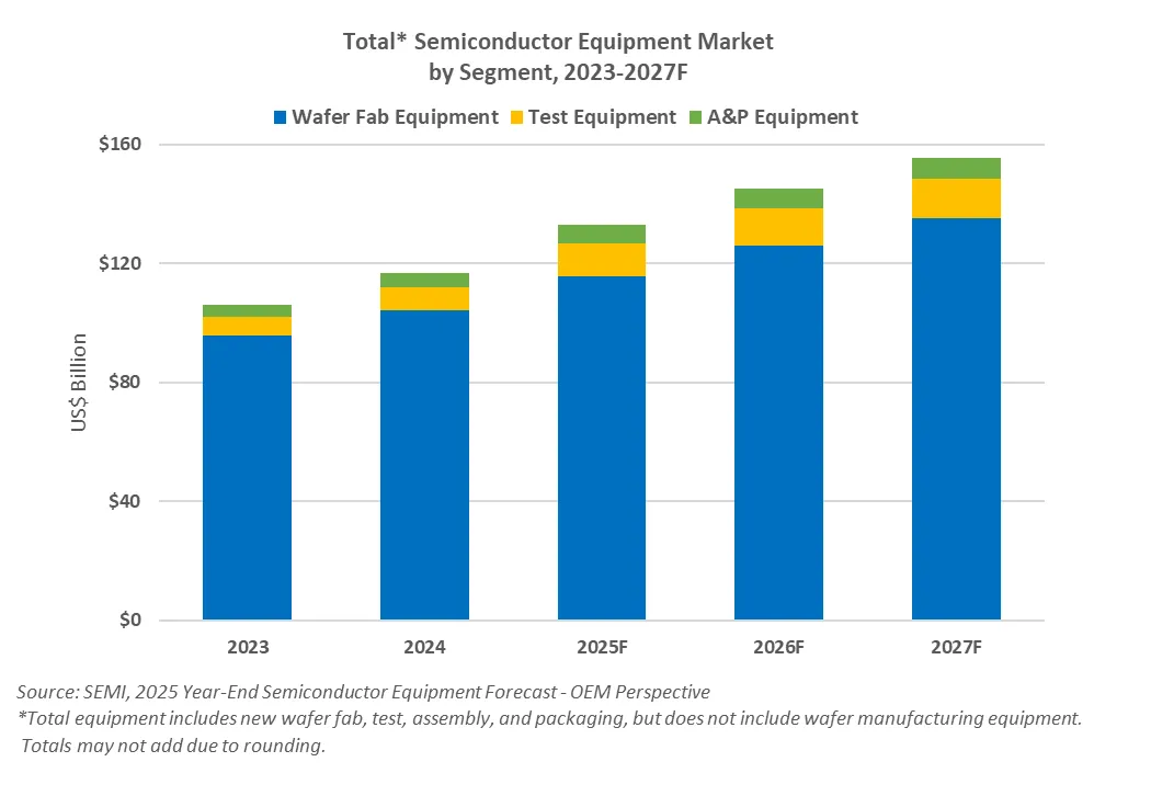
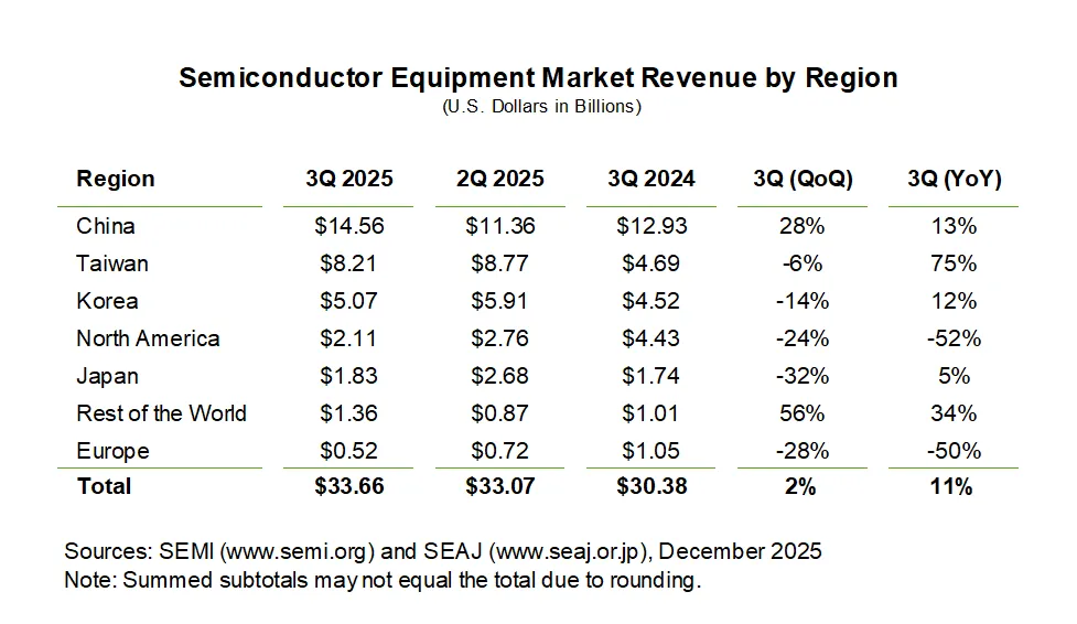
 “Global semiconductor equipment billings year-to-date have reached nearly $100 billion – a record through three quarters – reflecting the industry’s sustained momentum and commitment to invest in technology innovation,” said Ajit Manocha, SEMI President and CEO. “Strong AI demand continues to drive spending in advanced logic and memory segments, as well as in packaging applications geared toward energy efficiency. This positive trajectory underscores the critical role semiconductors play in shaping a smarter and more connected world that powers next-generation digital solutions.”
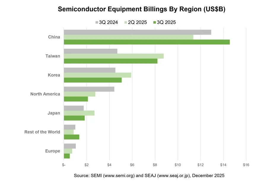
 “January through September silicon shipments registered a significant year-on-year increase primarily driven by the growth of 300 mm shipments for advanced logic, cloud infrastructure, and memory demand,” said Lee Chungwei (李崇偉), Chairman of SEMI SMG and Vice President and Chief Auditor at GlobalWafers. “AI empowers significant investments expansion in advanced processes contributing to the wafer demand growth.”
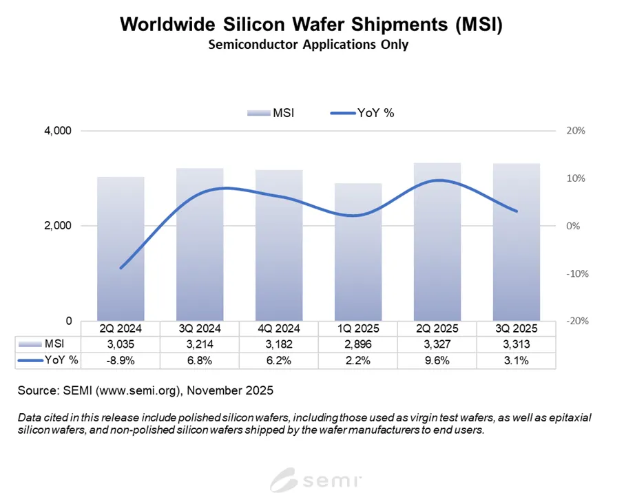
 In 2025, the increase in silicon wafer shipments has been supported by strong AI-related growth, including advanced epitaxial wafers for leading edge logic devices and polished wafers for high bandwidth memory (HBM). Wafer shipments for non-AI applications, however, are just beginning to demonstrate a gradual recovery from the recent downcycle. The steady growth is expected to continue through 2028, driven by AI’s expanding compute footprint in data centers and at the edge.
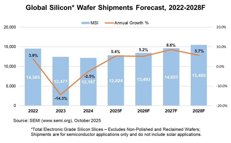
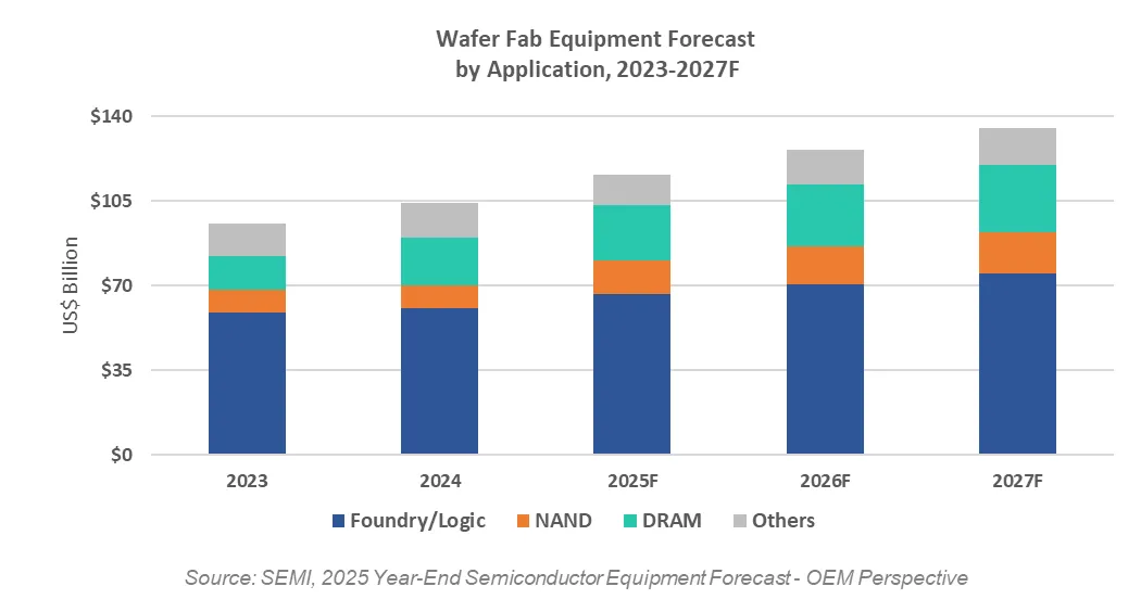
 Worldwide 300mm fab equipment spending is expected to surpass $100 billion for the first time in 2025, growing 7% to $107 billion. The report projects investment will increase 9% to $116 billion in 2026, 4% to $120 billion in 2027, and 15% to $138 billion in 2028.
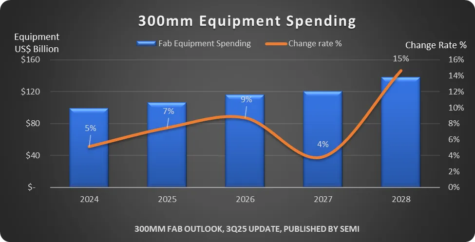
 “The electronic design automation (EDA) industry continues to report strong year-over-year revenue growth in Q2 2025,” said Walden C. Rhines, Executive Sponsor of the SEMI Electronic Design Market Data report. “Product categories including Computer-Aided Engineering (CAE), Printed Circuit Board and Multi-Chip Module, Semiconductor IP, and Services reported increases, with CAE and Services showing double digit gains. Geographic regions including Americas, EMEA, and APAC reported growth in Q2, even hitting double digits in Americas and EMEA.”
 “The global semiconductor equipment market has followed record billings of $117 billion in 2024 with a strong first half of 2025, registering more than $65 billion in revenue,” said Ajit Manocha, SEMI President and CEO. “Chipmakers continue to invest in production capacity to support advanced logic and memory innovation powering the AI wave, as well as key projects to bolster regional supply chain resilience.”
 “Following strong growth in 2024, global semiconductor manufacturing equipment sales are forecast to expand again this year and set a new record in 2026,” said Ajit Manocha, SEMI president and CEO. “While the semiconductor industry is closely monitoring macroeconomic uncertainty, AI-fueled demand for chip innovations is driving investments in capacity expansions and leading-edge production.”
 “The electronic design automation (EDA) industry once again reported strong year-over-year revenue growth in Q1 2025,” said Walden C. Rhines, Executive Sponsor of the SEMI Electronic Design Market Data report. “Product Categories CAE, IC Physical Design and Verification, and PCB & MCM reported single digit increases, with Semiconductor IP and Services reporting significant double-digit increases. All geographic regions reported growth in Q1, with Americas, EMEA, and Japan reporting double digit growth.”