
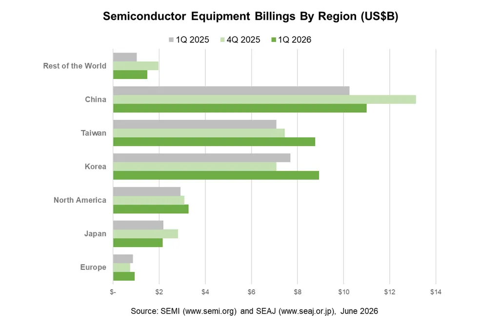
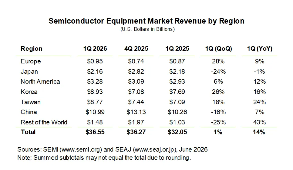
Record Quarterly Equipment Billings Reflect Continued AI-Driven Investment
MILPITAS, Calif. – June 4, 2026 – SEMI, the industry association serving the global semiconductor and electronics design and manufacturing supply chain, today announced in its Worldwide Semiconductor Equipment Market Statistics (WWSEMS) report that global semiconductor equipment billings increased 14% year-over-year to US$36.55 billion in the first quarter of 2026. First quarter 2026 billings registered a 1% quarter-over-quarter growth.
Record quarterly billings were driven by continued AI-related investment, including capacity expansion and technology upgrades supporting leading-edge logic, DRAM, and advanced packaging.
 “The strong start to 2026 reflects continued industry investment in the capacity and infrastructure needed to support AI-driven semiconductor growth,” said Ajit Manocha, SEMI President and CEO. “Record first-quarter billings highlight ongoing momentum in leading-edge manufacturing and advanced packaging.”
Compiled from data submitted by members of SEMI and the Semiconductor Equipment Association of Japan (SEAJ), the WWSEMS report is a summary of the monthly billings figures for the global semiconductor equipment industry.
The following are quarterly billings data in billions of U.S. dollars, with quarter-over-quarter and year-over-year changes by region:
About SEMI Equipment Market Data Subscription (EMDS)
The Equipment Market Data Subscription (EMDS) from SEMI provides comprehensive market data for the global semiconductor equipment market. A subscription includes three reports:
- Monthly SEMI North American Billings Report, an early perspective of equipment market trends
- Monthly Worldwide Semiconductor Equipment Market Statistics (WWSEMS), a detailed report of semiconductor equipment billings for seven regions and more than 22 market segments
- Bi-annual Total Semiconductor Equipment Forecast – OEM Perspective, an outlook for the semiconductor equipment market
Download a sample EMDS report.
For more information about the report or to subscribe, please contact the SEMI Market Intelligence Team at [email protected]. More details are also available on the SEMI Market Data webpage.
Follow SEMI Market Intelligence
Follow SEMI
About SEMI
SEMI® is the global industry association connecting over 4,000 companies and 1.5 million professionals worldwide across the semiconductor and electronics design and manufacturing supply chain. We accelerate member collaboration on solutions to top industry challenges through Advocacy, Workforce Development, Sustainability, Supply Chain Management and other programs. Our SEMICON® expositions and events, technology communities, standards and market intelligence help advance our members’ business growth and innovations in design, devices, equipment, materials, services and software, enabling smarter, faster, more secure electronics. Visit www.semi.org, contact a regional office, and connect with SEMI on LinkedIn and X to learn more.
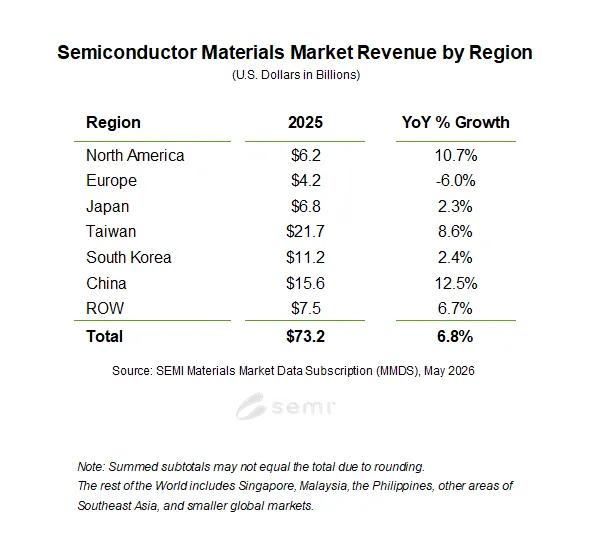
 Wafer fabrication materials revenue increased 5.4% to $45.8 billion. Lithography-related materials, including photomask, photoresist and ancillaries, along with wet chemicals, posted strong double-digit growth as higher process intensity and tighter lithography requirements continued to increase materials consumption.
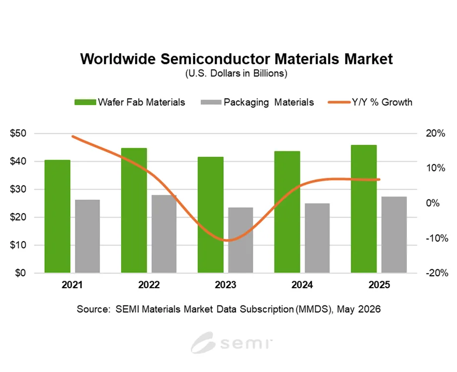
 “The electronic design automation (EDA) industry continues to report strong year-over-year revenue growth in Q4 2025,” said Walden C. Rhines, Executive Sponsor of the SEMI Electronic Design Market Data report. “Product categories CAE, PCB and MCM, Semiconductor IP (SIP), and Services all reported gains. Geographic regions including Americas, EMEA, and APAC reported growth in Q4, with a double digit increase in Americas and APAC.”
 In 2025, the global front-end semiconductor equipment market posted solid growth, with wafer processing equipment sales increasing 12% and other front-end segments rising 13%. The expansion was driven primarily by continued investment in leading-edge logic and memory capacity, supported by AI-related demand and ongoing node and technology migrations.
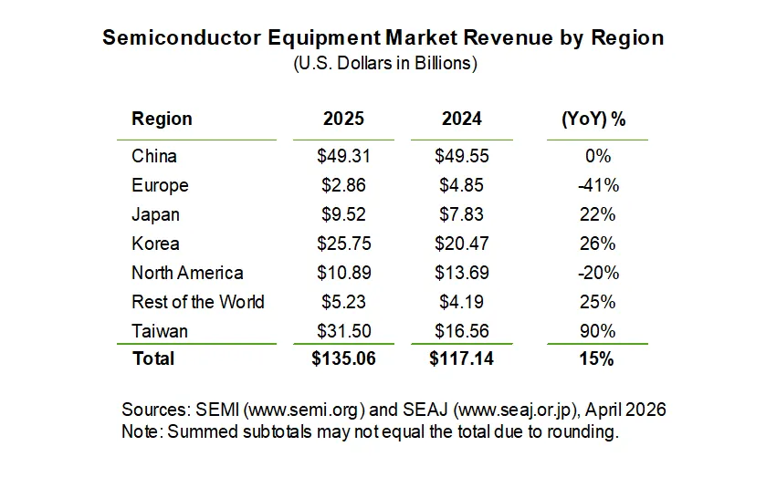

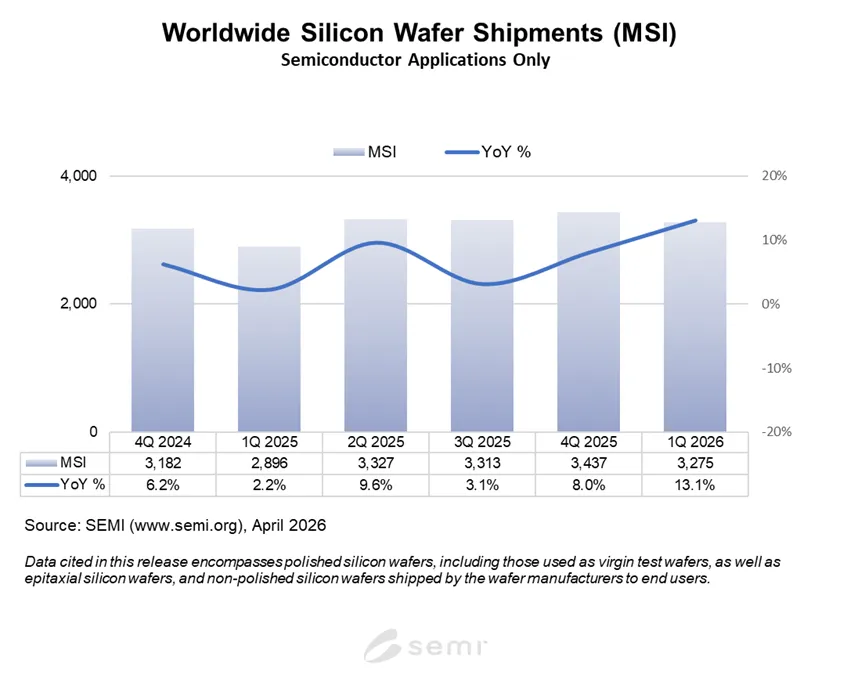
 2025 marks an inflection year for wafer shipments, with silicon MSI resuming growth supported by strong demand for advanced epitaxial wafers in logic and polished wafers for high-bandwidth memory (HBM), driven by AI applications. Softness in wafer revenue is mostly attributed to the slow momentum in traditional semiconductor applications where the demand and pricing environment are yet to improve.
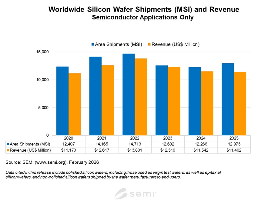
 “The electronic design automation (EDA) industry continues to report strong year-over-year revenue growth in Q3 2025,” said Walden C. Rhines, Executive Sponsor of the SEMI Electronic Design Market Data report. “All product categories reported increases, with Semiconductor IP (SIP) and Services showing double digit gains. Geographic regions including Americas, EMEA, and APAC reported growth in Q3, with a double digit increase in APAC.”