downloadGroupGroupnoun_press release_995423_000000 copyGroupnoun_Feed_96767_000000Group 19noun_pictures_1817522_000000Member company iconResource item iconStore item iconGroup 19Group 19noun_Photo_2085192_000000 Copynoun_presentation_2096081_000000Group 19Group Copy 7noun_webinar_692730_000000Path
Skip to main content
Default Banner Image

Market Intelligence

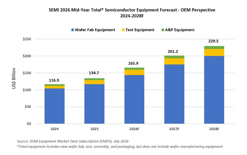
MILPITAS, Calif. — July 14, 2026 — Global sales of total semiconductor manufacturing equipment by original equipment manufacturers (OEMs) are forecast to reach a record high of $165.9 billion in 2026, increasing 23.2% year-on-year, SEMI announced today in its Mid-Year Total Semiconductor Equipment Forecast – OEM Perspective. Growth momentum is expected to continue through 2028, with total equipment sales forecast to reach a record $229.5 billion, marking five consecutive years of growth as AI-driven demand reshapes semiconductor manufacturing investment. 

The stronger outlook reflects accelerating investment in AI infrastructure, leading-edge logic, advanced memory, and back-end technologies needed to support higher compute density, high bandwidth memory (HBM)-related investment, and increasingly complex device architectures.

“AI is accelerating demand for more powerful and efficient chips, driving increased investment across the semiconductor capital equipment market,” said Ajit Manocha, SEMI president and CEO. “The mid-year forecast points to a higher equipment spending trajectory as chipmakers invest in the leading-edge logic, advanced memory, test and packaging capabilities required for the AI era.”

Semiconductor Equipment Sales by Segment 

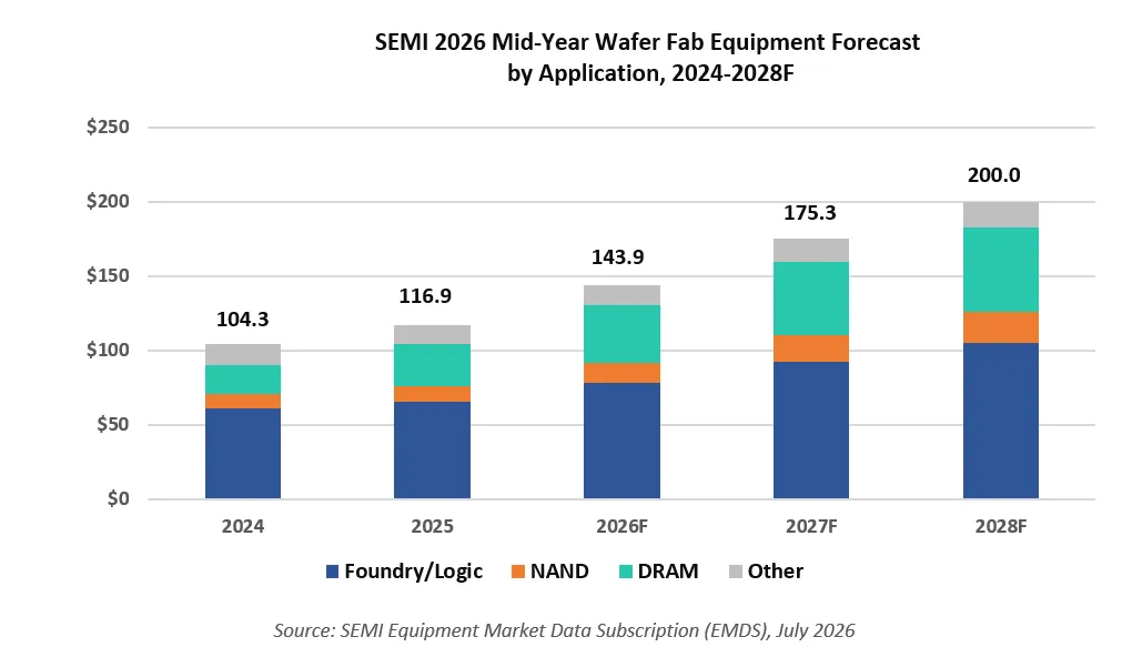
After registering a record $116.9 billion in sales last year, the Wafer Fab Equipment (WFE) segment, which includes wafer processing, mask/reticle, and fab facilities equipment, is projected to increase 23.1% to $143.9 billion in 2026. This represents a significant upward revision from SEMI’s 2025 year-end forecast and reflects stronger investment in advanced memory, especially HBM-related DRAM technologies, and leading-edge logic applications. WFE segment sales are projected to expand 21.8% in 2027 and 14.1% in 2028 to reach the $200 billion mark, as manufacturers accelerate capacity expansion and technology migration for AI-related workloads.

AI-related semiconductor demand is also driving expansion in back-end equipment. After surging 55.3% in 2025, semiconductor test equipment sales are projected to increase 31.0% to $15.3 billion in 2026, marking a strong upward revision from SEMI’s 2025 year-end forecast. Assembly and packaging equipment sales, which increased 20.8% in 2025, are projected to rise 9.6% to $6.7 billion in 2026, broadly in line with the prior forecast. Growth is expected to continue through 2028, with test equipment reaching $20.8 billion and assembly and packaging equipment reaching $8.6 billion, supported by increasing device complexity, advanced and heterogeneous packaging adoption, and more rigorous performance and reliability requirements for AI and HBM devices.

WFE Sales by Application

WFE sales for foundry and logic applications are expected to increase 18.9% year-over-year to $78.0 billion in 2026, driven by advanced-node capacity buildouts for AI accelerators, high-performance computing, and premium mobile processors. The segment is forecast to grow 18.1% in 2027 and 13.6% in 2028, reaching $104.7 billion, as the industry advances toward high-volume manufacturing at the 2nm gate-all-around node.

Memory-related equipment spending is projected to expand significantly through 2028, supported by HBM demand, advanced DRAM node migration, and NAND technology transitions. DRAM equipment sales are projected to rise 39.0% to $38.8 billion in 2026, followed by 27.4% growth in 2027 and 15.0% growth in 2028, reaching $56.9 billion. NAND equipment sales are expected to grow 30.7% to $13.9 billion in 2026, then increase 31.1% in 2027 and 14.5% in 2028, reaching $20.8 billion, driven by 3D NAND layer migration and investment in higher-density architectures.

Semiconductor Equipment Sales by Region

China, Taiwan and Korea are expected to remain the top three destinations for equipment spending through 2028. China is projected to maintain the leading position over the forecast period, though growth is expected to moderate in 2026 following elevated investment levels in recent years. In Taiwan, spending is supported by leading-edge capacity builds for AI and high-performance computing, while Korea’s equipment spending is driven by advanced memory technologies, including HBM. Other regions tracked are expected to see equipment spending increase in 2027 and 2028, supported by regionalization efforts, government incentives and targeted specialty capacity expansions.

The SEMI forecast is based on collective input from top equipment suppliers, the SEMI Worldwide Semiconductor Equipment Market Statistics (WWSEMS) data collection program, and the industry-recognized SEMI World Fab Forecast database. 

About SEMI Market Data

The Equipment Market Data Subscription (EMDS) from SEMI provides comprehensive market data for the global semiconductor equipment market. A subscription includes three reports: 

  • Monthly SEMI North American Billings Report, an early perspective of equipment market trends
  • Monthly Worldwide Semiconductor Equipment Market Statistics (WWSEMS), a detailed report of semiconductor equipment billings for seven regions and more than 22 market segments
  • Bi-annual Total Semiconductor Equipment Forecast – OEM Perspective, an outlook for the semiconductor equipment market

Download a sample EMDS report.

For more information about the report or to subscribe, please contact the SEMI Market Intelligence Team at [email protected]. More details are also available on the SEMI Market Data webpage.  

Follow SEMI Market Intelligence

Follow SEMI 

About SEMI

SEMI® is the global industry association connecting over 4,000 companies and 1.5 million professionals worldwide across the semiconductor and electronics design and manufacturing supply chain. We accelerate member collaboration on solutions to top industry challenges through Advocacy, Workforce Development, Sustainability, Supply Chain Management and other programs. Our SEMICON® expositions and events, technology communities, standards and market intelligence help advance our members’ business growth and innovations in design, devices, equipment, materials, services and software, enabling smarter, faster, more secure electronics. Visit www.semi.org, contact a regional office, and connect with SEMI on LinkedIn and X to learn more.

MILPITAS, Calif. - July 7, 2026 - SEMI and TechSearch International today announced the release of the 2026 edition of the Worldwide Assembly & Test Facility Database, a comprehensive resource tracking semiconductor back-end manufacturing facilities operated by integrated device manufacturers (IDMs) and outsourced semiconductor assembly and test (OSAT) companies worldwide.

The 2026 edition covers more than 820 facilities, up from 750 in the 2025 edition, and adds new fields that help users analyze not only where facilities are located and what assembly and test services they provide, but also the materials, platforms, technologies and end markets they support.

Based on the new classifications, more than 360 facilities report compound semiconductor capabilities, including sites supporting silicon carbide (SiC), gallium nitride (GaN), gallium arsenide (GaAs) and indium phosphide (InP). More than 170 facilities identify AI and high-performance computing (HPC) among their end-market focus, while more than 70 facilities support photonics and optical applications. The new fields also capture substrate and interposer platforms along with broader technology and module capabilities, providing clearer visibility into how global back-end infrastructure is aligning with emerging demand.

“AI infrastructure, photonics and compound semiconductors are expanding the range of capabilities required across semiconductor assembly and test,” said Clark Tseng, Senior Director of Market Intelligence at SEMI. “The 2026 database gives users a more detailed view of which facilities support these technologies and end markets, helping them assess supply-chain exposure, identify manufacturing partners and track the evolution of global back-end capabilities.”

The 2026 edition includes the following updates and enhancements:

  • Expanded Global Coverage: More than 820 facilities worldwide, an increase of more than 70 facilities from the 2025 edition. The largest additions to database coverage were in China and Taiwan.
  • Compound Semiconductor Visibility: New fields identify whether facilities support compound semiconductors and specify material types including SiC, GaN, GaAs and InP.
  • End-Market Focus: New classifications provide insight into facilities supporting AI/HPC, automotive, mobile and consumer, industrial, networking and telecom, photonics and optical, and other end markets.
  • Substrate and Interposer Platforms: New data identifies capabilities across laminate substrates, redistribution layers (RDL), ceramic substrates, silicon interposers and leadframes.
  • Technology and Module Capabilities: Expanded facility-level descriptions provide additional detail on advanced packaging, modules, test services and specialized technology capabilities.
  • Updated Facility Profiles: The database continues to provide current information on facility status, ownership, location, plant type, assembly and test capabilities, device focus, automotive certification and operating history.
  • Updated OSAT Market Benchmarks: The 2026 edition includes updated top 10 OSAT capital expenditure and top 20 OSAT revenue rankings.

The database supports semiconductor manufacturers, equipment and materials suppliers, packaging and test providers, investors, government agencies and analysts seeking to map global manufacturing footprints, compare facility-level capabilities, identify potential partners, evaluate regional concentration and monitor facility openings, closures, expansions and ownership changes.

To access the Worldwide Assembly & Test Facility Database, visit https://www.semi.org/en/products-services/market-data/ww-assembly-test-facility-database. For more information on the report or to subscribe, please contact the SEMI Market Intelligence Team at [email protected]. More details are also available on the SEMI Market Data webpage.  

Follow SEMI Market Intelligence

Follow SEMI 

About SEMI

SEMI® is the global industry association connecting over 4,000 companies and 1.5 million professionals worldwide across the semiconductor and electronics design and manufacturing supply chain. We accelerate member collaboration on solutions to top industry challenges through Advocacy, Workforce Development, Sustainability, Supply Chain Management and other programs. Our SEMICON® expositions and events, technology communities, standards and market intelligence help advance our members’ business growth and innovations in design, devices, equipment, materials, services and software, enabling smarter, faster, more secure electronics. Visit www.semi.org, contact a regional office, and connect with SEMI on LinkedIn and X to learn more.  

About TechSearch International

TechSearch International, Inc., founded in 1987, is a market research leader specializing in technology trends in microelectronics packaging and assembly. Multi- and single-client services encompass technology licensing, strategic planning, and market and technology analysis. TechSearch International professionals have an extensive network of ~20,000 contacts in North America, Asia, and Europe. For more information, contact TechSearch International at [email protected] or tel: 512-372-8887 or see www.techsearchinc.com. Follow us on LinkedIn.


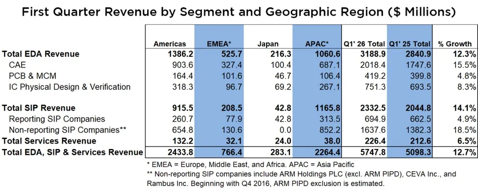
MILPITAS, Calif. — July 13, 2026 — Electronic System Design (ESD) industry revenue increased 12.7% to $5,747.8 million in the first quarter of 2026 from the $5,098.3 million registered in the first quarter of 2025, the ESD Alliance, a SEMI Technology Coalition, announced today in its latest Electronic Design Market Data (EDMD) report. The four-quarter moving average rose 10.3%, based on a comparison of the most recent four quarters to the prior four.

A black and white image of a number

Description automatically generated with medium confidence“The electronic design automation industry continued to report strong year-over-year revenue growth in Q1 2026,” said Walden C. Rhines, Executive Sponsor of the SEMI Electronic Design Market Data report and Chief Executive Officer of Silvaco Group, Inc. “All product categories reported gains, with Computer-Aided Engineering and Semiconductor IP showing double digit growth. The Americas, EMEA, and APAC geographic regions reported growth in Q1, with double digit increases in EMEA and APAC.”

The companies tracked in the EDMD report employed 72,544 people globally in Q1 2026, a 12.6% increase over the Q1 2025 headcount of 64,403 and up 1.1% compared to Q4 2025.

The quarterly EDMD report contains detailed revenue information within the following category and geographic breakdowns. 
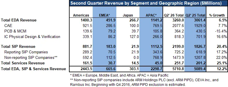
 

Revenue by Product and Application Category – Year-Over-Year Change

  • Computer-Aided Engineering (CAE) revenue increased 15.5% to $2,018.4 million. The four-quarter CAE moving average increased 13.1%. 
  • IC Physical Design and Verification revenue increased 8.3% to $751.3 million. The four-quarter moving average for the category decreased 0.9%. 
  • Printed Circuit Board and Multi-Chip Module (PCB and MCM) revenue rose 4.8% to $419.2 million. The four-quarter moving average for PCB and MCM rose 4.3%.
  • Semiconductor Intellectual Property (SIP) revenue increased 14.1% to $2,332.5 million. The four-quarter SIP moving average rose 13.7%.
  • Services revenue increased 6.5% to $226.4 million. The four-quarter Services moving average rose 11.9%.

Revenue by Region – Year-Over-Year Change

  • The Americas, the largest reporting region by revenue, procured $2,433.8 million of electronic system design products and services in Q1 2026, a 10.2% increase. The four-quarter moving average for the Americas rose 9.8%. 
  • Europe, Middle East, and Africa (EMEA) procured $766.4 million of electronic system design products and services in Q1 2026, a 17.6% increase. The four-quarter moving average for EMEA grew 10.9%. 
  • Japan’s procurement of electronic system design products and services decreased 9.9% to $283.1 million in Q1 2026. The four-quarter moving average for Japan decreased 12.4%. 
  • Asia Pacific (APAC) procured $2,264.4 million of electronic system design products and services in Q1 2026, a 17.7% increase. The four-quarter moving average for APAC grew 14.5%. 

About the EDMD Report

The ESD Alliance Electronic Design Market Data (formerly the Market Statistics Service) report presents Electronic Design Automation (EDA), SIP and Services industry revenue data quarterly. Both public and private companies contribute data to the report available from SEMI. Each quarterly report is published approximately three months after quarter close. EDMD report data is segmented as follows: 

  • Revenue by product category (CAE, IC Physical Design and Verification, SIP, PCB and MCM Layout, and Services) including numerous detailed sub-categories
  • Revenue by geographic region (Americas, EMEA, Japan and APAC)
  • Total employment at participating companies

For information about SEMI market research reports, visit the SEMI Market Research Reports and Databases Catalog

About the Electronic System Design Alliance

The Electronic System Design (ESD) Alliance, a SEMI Technology Coalition, is the central voice to communicate and promote the value of the semiconductor design ecosystem as a vital component of the global electronics industry. As an international association of companies providing goods and services throughout the semiconductor design ecosystem, it is a forum to address technical, marketing, economic and legislative issues affecting the entire industry. For more information about the ESD Alliance, visit http://esd-alliance.org.

Follow the ESD Alliance

About SEMI

SEMI® is the global industry association connecting over 4,000 companies and 1.5 million professionals worldwide across the semiconductor and electronics design and manufacturing supply chain. We accelerate member collaboration on solutions to top industry challenges through Advocacy, Workforce Development, Sustainability, Supply Chain Management and other programs. Our SEMICON® expositions and events, technology communities, standards and market intelligence help advance our members’ business growth and innovations in design, devices, equipment, materials, services and software, enabling smarter, faster, more secure electronics. Visit www.semi.org, contact a regional office, and connect with SEMI on LinkedIn and X to learn more.

The information supplied by the ESD Alliance is believed to be accurate and reliable, but the ESD Alliance assumes no responsibility for any errors that may appear in this document. All trademarks and registered trademarks are the property of their respective owners.

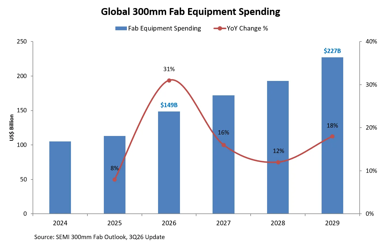
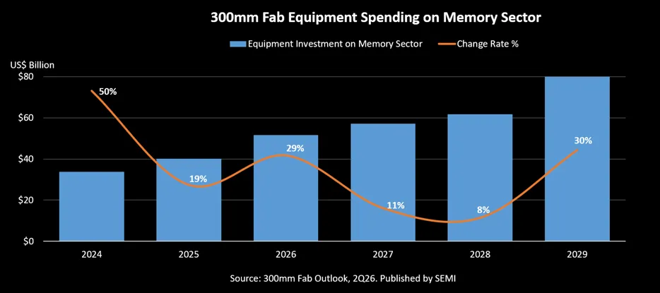
MILPITAS, Calif. – June 29, 2026 – Worldwide 300mm fab equipment investment in the memory sector is projected to surpass $50 billion for the first time in 2026, rising 29% to $52 billion before increasing another 11% to $57 billion in 2027, SEMI reported today in its latest 300mm Fab Outlook. The growth reflects continued AI-driven demand for advanced memory, supported by rising investment in AI infrastructure, data centers, and next-generation computing systems.

Looking further out, global 300mm fab equipment spending in the memory sector is expected to grow at a 19% CAGR from 2024 to 2029. Worldwide 300mm memory capacity is also projected to increase, reaching 4.1 million wafers per month in 2026 and 4.2 million wafers per month in 2027.

“Strong demand for high bandwidth memory and other advanced memory technologies is reshaping investment priorities across the semiconductor supply chain,” said Ajit Manocha, SEMI President and CEO. “As AI infrastructure expands, memory manufacturers are accelerating investments in both capacity and technology migration to support the next wave of data-intensive applications.”

Memory Segment Growth

The 2Q26 edition of the SEMI 300mm Fab Outlook includes an increased projection in 300mm fab equipment spending in the memory sector driven by continued upward capital expenditure plans among leading cloud service providers and strong demand for AI accelerators. DRAM equipment spending is expected to grow 29% to $37 billion in 2026, supported by strong HBM and DDR5 demand for GPUs and other AI accelerators. Equipment spending on 3D NAND is also projected to rise 28% to $14 billion in 2026, supported by increasing data storage requirements tied to AI deployment.

Continued investment in advanced-node DRAM and higher-layer 3D NAND is supporting a stronger memory capacity outlook, which has been revised upward in the 2Q26 edition of the SEMI 300mm Fab Outlook. Effective capacity growth, however, remains moderated by technology migration and process complexity, including advanced-node DRAM, HBM, and higher-layer NAND transitions.

The SEMI 300mm Fab Outlook lists 413 facilities and lines globally. The report reflects 155 updates and addition of 7 new fabs/lines projects since its last publication in March 2026. 

For more information on the report or to subscribe, please contact the SEMI Market Intelligence Team at [email protected]. More details are also available on the SEMI Market Data webpage.  

Follow SEMI Market Intelligence

Follow SEMI 

About SEMI

SEMI® is the global industry association connecting over 4,000 companies and 1.5 million professionals worldwide across the semiconductor and electronics design and manufacturing supply chain. We accelerate member collaboration on solutions to top industry challenges through Advocacy, Workforce Development, Sustainability, Supply Chain Management and other programs. Our SEMICON® expositions and events, technology communities, standards and market intelligence help advance our members’ business growth and innovations in design, devices, equipment, materials, services and software, enabling smarter, faster, more secure electronics. Visit www.semi.org, contact a regional office, and connect with SEMI on LinkedIn and X to learn more.  


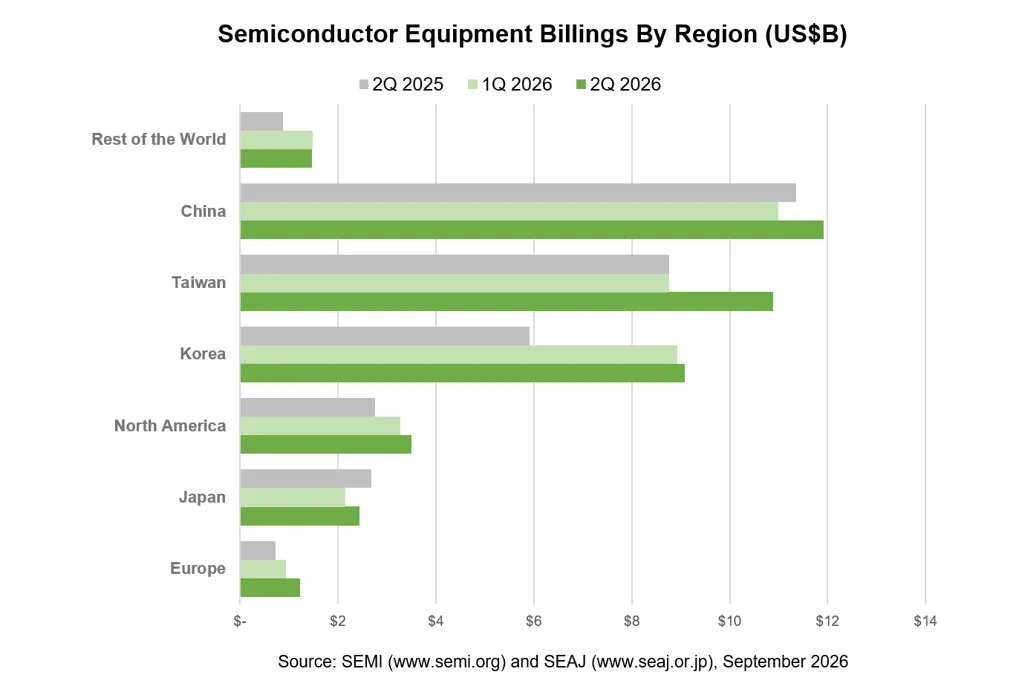
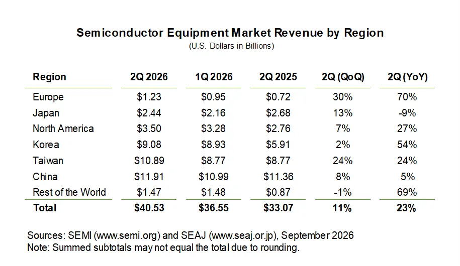
MILPITAS, Calif. – June 4, 2026 – SEMI, the industry association serving the global semiconductor and electronics design and manufacturing supply chain, today announced in its Worldwide Semiconductor Equipment Market Statistics (WWSEMS) report that global semiconductor equipment billings increased 14% year-over-year to US$36.55 billion in the first quarter of 2026. First quarter 2026 billings registered a 1% quarter-over-quarter growth.

Record quarterly billings were driven by continued AI-related investment, including capacity expansion and technology upgrades supporting leading-edge logic, DRAM, and advanced packaging. 

“The strong start to 2026 reflects continued industry investment in the capacity and infrastructure needed to support AI-driven semiconductor growth,” said Ajit Manocha, SEMI President and CEO. “Record first-quarter billings highlight ongoing momentum in leading-edge manufacturing and advanced packaging.”
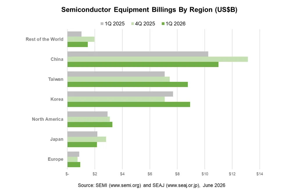
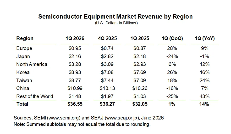
 

Compiled from data submitted by members of SEMI and the Semiconductor Equipment Association of Japan (SEAJ), the WWSEMS report is a summary of the monthly billings figures for the global semiconductor equipment industry. 

The following are quarterly billings data in billions of U.S. dollars, with quarter-over-quarter and year-over-year changes by region:


About SEMI Equipment Market Data Subscription (EMDS)

The Equipment Market Data Subscription (EMDS) from SEMI provides comprehensive market data for the global semiconductor equipment market. A subscription includes three reports: 

  • Monthly SEMI North American Billings Report, an early perspective of equipment market trends
  • Monthly Worldwide Semiconductor Equipment Market Statistics (WWSEMS), a detailed report of semiconductor equipment billings for seven regions and more than 22 market segments
  • Bi-annual Total Semiconductor Equipment Forecast – OEM Perspective, an outlook for the semiconductor equipment market

Download a sample EMDS report.

For more information about the report or to subscribe, please contact the SEMI Market Intelligence Team at [email protected]. More details are also available on the SEMI Market Data webpage.  

Follow SEMI Market Intelligence

Follow SEMI 

About SEMI

SEMI® is the global industry association connecting over 4,000 companies and 1.5 million professionals worldwide across the semiconductor and electronics design and manufacturing supply chain. We accelerate member collaboration on solutions to top industry challenges through Advocacy, Workforce Development, Sustainability, Supply Chain Management and other programs. Our SEMICON® expositions and events, technology communities, standards and market intelligence help advance our members’ business growth and innovations in design, devices, equipment, materials, services and software, enabling smarter, faster, more secure electronics. Visit www.semi.org, contact a regional office, and connect with SEMI on LinkedIn and X to learn more.

MILPITAS, Calif. — May 27, 2026 — SEMI, the industry association serving the global semiconductor and electronics design and manufacturing supply chain, today announced the availability of a new industry research report focused on the glass core substrate market and trends, produced in collaboration with Global Net Corp. (GNC). The Glass Core Substrate Market and Development Trends Report examines the emerging market for glass core substrates, a potential next-generation packaging technology attracting increased attention as AI and high-performance computing (HPC) drive demand for larger and more advanced semiconductor packages.

“As chipmakers look for new ways to improve system performance beyond traditional device scaling, advanced packaging has become a critical area of innovation,” said Clark Tseng, Senior Director of Market Intelligence, SEMI. “Glass core substrates are being evaluated as one possible solution for future high-end packages because they may help support larger package sizes, finer interconnects, and improved dimensional stability compared to conventional package-substrate materials. This new report helps industry stakeholders understand where glass core substrates may fit in the next phase of packaging technology and what challenges must be addressed to achieve broader adoption.”

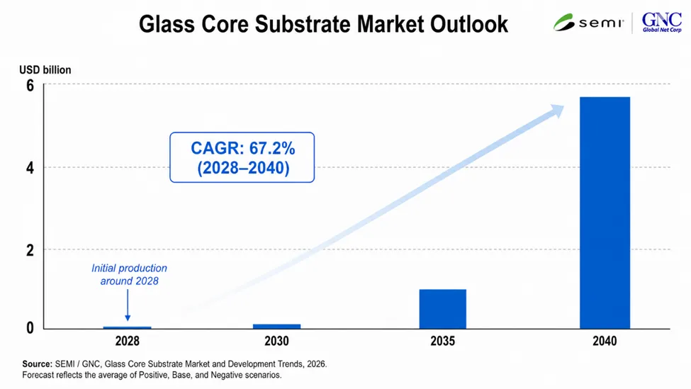
The report highlights increasing industry activity and investment around glass core substrates as companies prepare for the next phase of advanced packaging—providing an independent view of the technology’s market potential, development status, key players, and remaining barriers to commercialization. Under the report’s market-development scenarios, initial production could begin around 2028 in selected high-performance applications, with adoption expanding over time across larger and more complex package architectures. Based on the average of its Positive, Base, and Negative scenarios, the report projects a compound annual growth rate (CAGR) of 67.2% from 2028 to 2040. It also maps an increasingly active global development ecosystem, with companies and research organizations across Asia, North America and Europe advancing glass core substrate technologies.


Key topics covered in the report include:

  • Market outlook and adoption scenarios for glass core substrates 
  • Technology drivers and barriers to commercialization 
  • Expected applications in AI, HPC, advanced processors, co-packaged optics, and image sensors 
  • Company activities across substrates, glass materials, equipment, processing, inspection, and related supply-chain segments 
  • Development hubs, consortia, and supply-chain structure 
  • Forecast scenarios through 2040 

The Glass Core Substrate Market and Development Trends report is available in English and Japanese editions through SEMI Market Intelligence. Download the report.

For more information, please visit the Glass Core Substrate Market and Development Trends page or contact the SEMI Market Intelligence Team at [email protected].

Follow SEMI Market Intelligence

Follow SEMI 

About Global Net Corp.

Global Net Corp. is a Tokyo-based company serving the semiconductor and electronics industries. Established in 1990, the company provides wafer processing, equipment sales, consulting, technical seminars, research groups, and industry publishing services. Its technical and market coverage spans semiconductors, electronics, FPD, packaging, CMP, and related manufacturing processes.

About SEMI

SEMI® is the global industry association connecting over 4,000 companies and 1.5 million professionals worldwide across the semiconductor and electronics design and manufacturing supply chain. We accelerate member collaboration on solutions to top industry challenges through Advocacy, Workforce Development, Sustainability, Supply Chain Management and other programs. Our SEMICON® expositions and events, technology coalitions, standards and market intelligence help advance our members’ business growth and innovations in design, devices, equipment, materials, services and software, enabling smarter, faster, more secure electronics. Visit www.semi.org, contact a regional office, and connect with SEMI on LinkedIn and X to learn more.

MILPITAS, Calif. — May 12, 2026 — Global semiconductor materials market revenue increased 6.8% year-over-year to $73.2 billion in 2025, SEMI, reported today in its Materials Market Data Subscription (MMDS). Growth was supported by gains in both the wafer fab materials and packaging materials segments, reflecting higher process complexity, advanced-node demand, and continued investment in high-performance computing and high-bandwidth memory manufacturing. 

Wafer fabrication materials revenue increased 5.4% to $45.8 billion. Lithography-related materials, including photomask, photoresist and ancillaries, along with wet chemicals, posted strong double-digit growth as higher process intensity and tighter lithography requirements continued to increase materials consumption.

Packaging materials revenue grew 9.3% to $27.4 billion in 2025. Substrates and bonding wire led the increase, supported by higher gold prices in bonding wire and stronger demand for advanced substrates.

Taiwan remained the largest consumer of semiconductor materials for the 16th consecutive year, with revenue of $21.7 billion in 2025. China ranked second at $15.6 billion, supported by double-digit growth, followed by South Korea at $11.2 billion. All regions except Europe posted year-over-year increases, with China and North America recording the strongest growth among major regions.

The Materials Market Data Subscription (MMDS) from SEMI provides annual revenue with 10 years of historical data and a two-year forecast. The annual subscription includes quarterly updates for the materials segment and reports revenue for seven market regions (North America, Europe, Japan, Taiwan, South Korea, China and Rest of World). The report also features detailed historical data for silicon shipments and revenues for photoresist, photoresist ancillaries, process gases and lead frames.

For more information about the report or to subscribe, please contact the SEMI Market Intelligence Team at [email protected]. More details are also available on the SEMI Market Data webpage.  

Download a sample of the MMDS report

Follow SEMI Market Intelligence

Follow SEMI 

About SEMI

SEMI® is the global industry association connecting over 4,000 companies and 1.5 million professionals worldwide across the semiconductor and electronics design and manufacturing supply chain. We accelerate member collaboration on solutions to top industry challenges through Advocacy, Workforce Development, Sustainability, Supply Chain Management and other programs. Our SEMICON® expositions and events, technology communities, standards and market intelligence help advance our members’ business growth and innovations in design, devices, equipment, materials, services and software, enabling smarter, faster, more secure electronics. Visit www.semi.org, contact a regional office, and connect with SEMI on LinkedIn and X to learn more.

Semiconductor industry leader takes the helm to accelerate Beneq’s next phase of growth in atomic layer deposition

Espoo, Finland, 8 May, 2026 – Beneq Oy, the home of atomic layer deposition (ALD), today announced the appointment of Dr. Jason Harrison as Chief Executive Officer. Dr. Harrison succeeds Dr. Tommi Vainio and will lead Beneq into its next phase of growth across semiconductor, optical, and emerging technology markets.

A Strategic Leadership Transition
Beneq enters its next phase of growth from a position of strong commercial momentum. Recent milestones include the qualification of the Beneq Transform® cluster tool for volume production of GaN power and RF filter devices; the introduction of Beneq Transmute™ and Beneq Transform® XP, both engineered for high-volume manufacturing (HVM) of specialty semiconductors; growing adoption of the P-Series for coating critical chamber parts in advanced node devices; and selection of the C2R™ for AR waveguide production in next-generation XR optics.

Against this backdrop, the Board of Directors has determined that the time is right to align executive leadership with the company's evolving strategic priorities. As part of this transition, Dr. Tommi Vainio has decided to step down as CEO to pursue other opportunities. The Board of Directors extends its sincere thanks to Tommi, whose leadership advanced Beneq's technology platform, strengthened its market position in thin film deposition, and guided the company through important stages of its development.

A Proven Leader for a Scaling ALD Business
Dr. Harrison brings extensive global experience across the semiconductor and advanced technology sectors. He holds a Ph.D. in Quantum Chemistry and has built a distinguished career spanning device manufacturing, process development, and equipment solutions, with senior leadership roles at Intel, Lam Research, Veeco, and Applied Materials covering research and development, new product introduction, global account management, and business unit leadership. This combination of technical depth and commercial acumen positions him to scale Beneq’s commercial execution and growth across its global customer base.

Looking Ahead
Under Jason’s leadership, Beneq will accelerate strategic execution across its expanding portfolio, deepen customer engagement across North America, Asia, and Europe, and continue investing in innovative ALD solutions from R&D to HVM to deliver long-term value to customers, employees, and stakeholders.

Dr. Patrick Rabinzohn, Member of the Board of Directors, Beneq, said: “Jason brings the technical depth, the business and account management experience, and the global perspective Beneq needs at this stage of its growth. His academic background and compelling track record across the semiconductor industry positions Jason to build on the momentum the company generated especially.”

Dr. Jason Harrison, Chief Executive Officer, Beneq, added: “Beneq has a strong technology foundation, a talented team, and a growing pipeline of customers in some of the most important markets in semiconductors and optics. I look forward to working with the team to accelerate execution and deliver on the trust our customers place in us.”

About Beneq
Beneq pioneered industrial production of Atomic Layer Deposition (ALD) with the introduction of the first commercial ALD equipment in 1984. Today, Beneq advances ALD adoption and validation with a portfolio that includes the Beneq Transform®, Transform XP, Transform 300, and Transmute™ for specialty semiconductor device fabrication; TFS 200 and TFS 500 for R&D; the P400A, P800, and P1500 batch systems for coating critical semiconductor chamber components and complex part geometries; and spatial ALD platforms such as the C2R™ and roll-to-roll processing equipment. Headquartered in Espoo, Finland, Beneq enables ALD integration from lab to fab for semiconductors, optics, and functional coatings.

Press Contacts
Lie Luo
Head of Marketing
[email protected]

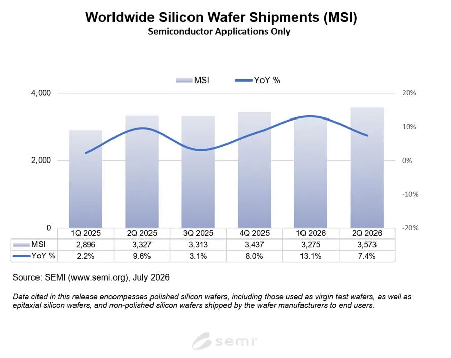
MILPITAS, Calif. — April 29, 2026 — The SEMI Silicon Manufacturers Group (SMG) reported today, in its quarterly analysis of the silicon wafer industry, that worldwide silicon wafer shipments increased 13.1% year-on-year to 3,275 million square inches (MSI) from the 2,896 MSI recorded during the same quarter of 2025. Sequentially, shipments declined 4.7% quarter-over-quarter from the 3,437 MSI recorded during the fourth quarter of 2025 in line with typical seasonality. 

“Silicon wafer demand related to AI data centers continues to be strong, including advanced logic and memory, and also now extending to power management devices,” said Ginji Yada, Chairman of SEMI SMG and Managing Executive Officer, General Manager, Sales and Marketing Division at SUMCO Corporation. “Overall, silicon wafer demand has improved, but the recovery is not uniform. Many device companies have noted improvements in the industrial semiconductor segment, and this is creating a more broad-based recovery as wafer inventory is absorbed. Weaker smartphone and PC shipments in the first quarter of this year may show the impact of tighter supply of memory due to AI high bandwidth memory (HBM) allocation decisions.”

Silicon wafers are the fundamental building material for the majority of semiconductors, which are vital components of all electronic devices. The highly engineered thin disks are produced in diameters of up to 300 mm and serve as the substrate material on which most semiconductors are fabricated.

The SMG is a sub-committee of the SEMI Electronic Materials Group (EMG) and is open to SEMI members involved in manufacturing polycrystalline silicon, monocrystalline silicon or silicon wafers (e.g., as cut, polished, epitaxial). The SMG facilitates collective efforts on issues related to the silicon industry, including the development of statistics about the silicon industry.

For more information, visit SEMI Worldwide Silicon Wafer Shipment Statistics.

Follow SEMI Market Intelligence

Follow SEMI 

About SEMI

SEMI® is the global industry association connecting over 4,000 companies and 1.5 million professionals worldwide across the semiconductor and electronics design and manufacturing supply chain. We accelerate member collaboration on solutions to top industry challenges through Advocacy, Workforce Development, Sustainability, Supply Chain Management and other programs. Our SEMICON® expositions and events, technology communities, standards and market intelligence help advance our members’ business growth and innovations in design, devices, equipment, materials, services and software, enabling smarter, faster, more secure electronics. Visit www.semi.org, contact a regional office, and connect with SEMI on LinkedIn and X to learn more.
 

MILPITAS, Calif. — April 13, 2026 — Electronic System Design (ESD) industry revenue increased 10.3% to $5,466.3 million in the fourth quarter of 2025 from the $4,955.2 million registered in the fourth quarter of 2024, the ESD Alliance, a SEMI Technology Community, announced today in its latest Electronic Design Market Data (EDMD) report. The four-quarter moving average rose 10.1%, based on a comparison of the most recent four quarters to the prior four.

“The electronic design automation (EDA) industry continues to report strong year-over-year revenue growth in Q4 2025,” said Walden C. Rhines, Executive Sponsor of the SEMI Electronic Design Market Data report. “Product categories CAE, PCB and MCM, Semiconductor IP (SIP), and Services all reported gains. Geographic regions including Americas, EMEA, and APAC reported growth in Q4, with a double digit increase in Americas and APAC.”

The companies tracked in the EDMD report employed 71,517 people globally in Q4 2025, a 13.8% increase over the Q4 2024 headcount of 62,833 but down 2.3% compared to Q3 2025. 

The quarterly EDMD report contains detailed revenue information within the following category and geographic breakdowns. 

Revenue by Product and Application Category – Year-Over-Year Change

  • Computer-Aided Engineering (CAE) revenue increased 9.4% to $1,887.4 million. The four-quarter CAE moving average increased 10.8%. 
  • IC Physical Design and Verification revenue decreased 2.6% to $777.2 million. The four-quarter moving average for the category decreased 5.1%. 
  • Printed Circuit Board and Multi-Chip Module (PCB and MCM) revenue rose 1.8% to $484.6 million. The four-quarter moving average for PCB and MCM rose 4.5%.
  • Semiconductor Intellectual Property (SIP) revenue increased 18.3% to $2,083.2 million. The four-quarter SIP moving average rose 17.4%.
  • Services revenue increased 19.6% to $233.9 million. The four-quarter Services moving average rose 15.9%.

Revenue by Region – Year-Over-Year Change

  • The Americas, the largest reporting region by revenue, procured $2,473.5 million of electronic system design products and services in Q4 2025, a 13.9% increase. The four-quarter moving average for the Americas rose 10.6%. 
  • Europe, Middle East, and Africa(EMEA) procured $683.4 million of electronic system design products and services in Q4 2025, a 9.8% increase. The four-quarter moving average for EMEA grew 9.4%. 
  • Japan’s procurement of electronic system design products and services decreased 18.8% to $258.5 million in Q4 2025. The four-quarter moving average for Japan decreased 7.4%. 
  • Asia Pacific (APAC) procured $2,050.8 million of electronic system design products and services in Q4 2025, an 11.3% increase. The four-quarter moving average for APAC grew 12.6%. 

About the EDMD Report

The ESD Alliance Electronic Design Market Data (formerly the Market Statistics Service) report presents Electronic Design Automation (EDA), SIP and Services industry revenue data quarterly. Both public and private companies contribute data to the report available from SEMI. Each quarterly report is published approximately three months after quarter close. EDMD report data is segmented as follows: 

  • Revenue by product category (CAE, IC Physical Design and Verification, SIP, PCB and MCM Layout, and Services) including numerous detailed sub-categories
  • Revenue by geographic region (Americas, EMEA, Japan and APAC)
  • Total employment at participating companies

For information about SEMI market research reports, visit the SEMI Market Research Reports and Databases Catalog.

About the Electronic System Design Alliance

The Electronic System Design (ESD) Alliance, a SEMI Technology Community, is the central voice to communicate and promote the value of the semiconductor design ecosystem as a vital component of the global electronics industry. As an international association of companies providing goods and services throughout the semiconductor design ecosystem, it is a forum to address technical, marketing, economic and legislative issues affecting the entire industry. For more information about the ESD Alliance, visit http://esd-alliance.org.

Follow the ESD Alliance

About SEMI

SEMI® is the global industry association connecting over 3,000 member companies and 1.5 million professionals worldwide across the semiconductor and electronics design and manufacturing supply chain. We accelerate member collaboration on solutions to top industry challenges through Advocacy, Workforce Development, Sustainability, Supply Chain Management and other programs. Our SEMICON® expositions and events, technology communities, standards and market intelligence help advance our members’ business growth and innovations in design, devices, equipment, materials, services and software, enabling smarter, faster, more secure electronics. Visit www.semi.org, contact a regional office, and connect with SEMI on LinkedIn and X to learn more.

The information supplied by the ESD Alliance is believed to be accurate and reliable, but the ESD Alliance assumes no responsibility for any errors that may appear in this document. All trademarks and registered trademarks are the property of their respective owners.