downloadGroupGroupnoun_press release_995423_000000 copyGroupnoun_Feed_96767_000000Group 19noun_pictures_1817522_000000Member company iconResource item iconStore item iconGroup 19Group 19noun_Photo_2085192_000000 Copynoun_presentation_2096081_000000Group 19Group Copy 7noun_webinar_692730_000000Path
Skip to main content
Default Banner Image

Packaging

ERS electronic, the industry leader of thermal management solutions for semiconductor manufacturing, today announced its fully automated panel-level packaging (PLP) system for 310×310 mm substrates. The machine integrates temporary carrier bonding, debonding, and detaping into a single automated platform at 13 panels per hour, eliminating inter-tool transfers across three thermally critical process steps. The first unit has been delivered to a leading semiconductor manufacturer for integration into its panel production line.

The machine is developed and manufactured at the company’s Advanced Packaging facility in Barbing, Germany. The facility combines ERS's 55 years of thermal management expertise with more than 30 years of in-house machine-building capability, following ERS's 2024 integration of a semiconductor specialist equipment engineering team.

ERS is considered an early adopter of panel-level packaging, as it shipped its first commercial panel-level tool to Fraunhofer IZM in Berlin in 2018. The 310×310 mm panel format is gaining traction across the industry because it improves substrate area utilisation significantly compared to 300 mm circular wafers. The panel-level packaging segment is projected to grow at a compound annual growth rate of over 40% over the next five years, according to Yole Group (1). As dual-carrier bonding and debonding workflows become increasingly important for backside processing in 3D IC, HBM and 2.5D IC packaging, ERS's integrated platform addresses these requirements in a single automated system.

In dual-carrier processes, bonding and debonding typically requires separate machines, often located at different points on the fab floor. Moving panels between them introduces handling steps, transit time, and the risk of substrate damage. ERS’s machine consolidates all three process steps within one platform, so panels move between process modules rather than between machines, thereby reducing handling time and risk without changes to the surrounding fab layout.

"Our new machine reflects our commitment to solving real manufacturing challenges. By integrating three process steps that have traditionally required separate tools into one automated platform, we're enabling customers to streamline production, improve process consistency, and achieve higher yield and throughput,” says Laurent Giai-Miniet, CEO of ERS electronic GmbH.

1 Source: Panel-Level Packaging 2026, Yole Group, 2026.

About ERS:
ERS electronic GmbH, based in the Munich suburb of Germering, has been providing innovative thermal management solutions to the semiconductor industry for more than 50 years. The company has gained an outstanding reputation, notably with its fast and accurate air cooling-based thermal chuck systems for wafer probing. In 2008, ERS extended its expertise to the Advanced Packaging market. Today, their fully automatic and manual debonding and warpage correction systems can be found on the production floors of most semiconductor manufacturers and OSATs worldwide.

Rolla, Missouri, USA — August 24, 2026 — Brewer Science, Inc., a global leader in advanced materials and process solutions for the semiconductor industry, will be showcasing its latest innovations in material solutions enabling next-generation technology at SEMICON Taiwan 2026, taking place September 2–4, 2026, in Taipei, Taiwan. Visit Brewer Science at Booth I2316 to discuss applications and specific solutions for artificial intelligence (AI), high-performance computing (HPC), and other advanced materials.

AI-driven patterning innovation: Learn how advanced materials enable high-selectivity patterning and support next-generation lithography in AI-driven semiconductor manufacturing.

2D materials integration breakthroughs: Discover new approaches for integrating fragile 2D semiconductors using low-temperature transfer and proven temporary bonding technologies.

Advanced packaging & heterogeneous integration: Explore materials solutions designed to support increasingly complex device architectures and multi-layer integration.

Engage with Brewer Science experts at Booth I2316: Discuss your challenges in patterning, advanced packaging, and emerging materials integration with our technical team.

"As AI pushes semiconductor design to new limits, our customers need materials that can keep pace," said Dr. Srikanth (Sri) Kommu, co-CEO of Brewer Science. "SEMICON Taiwan brings the industry together at exactly the right moment, and we're here to show how Brewer Science enables greater performance, scalability, and supply chain resilience.”

Technical Presentation Highlights

Navigating the Patterning Landscape in the Era of AI-Driven Semiconductor Manufacturing

Presented by Dr. Douglas Guerrero, Senior Technologist, Brewer Science

Artificial intelligence is driving one of the most rapid technology transformations in history, pushing semiconductor manufacturing to its limits. As chipmakers race to meet the demands of AI and HPC, both logic and memory architectures are becoming more complex, requiring increasingly sophisticated patterning materials.

Dr. Guerrero will explore how the industry is adapting to a shifting ecosystem, where advanced manufacturing capabilities are consolidating while the number of specialized materials providers continues to grow. He will highlight how Brewer Science leverages its advanced materials portfolio to support next-generation lithography and advanced packaging.

Key Takeaways:

AI is accelerating adoption of advanced semiconductor technologies

Patterning complexity is driving demand for highly engineered materials

High-selectivity materials are critical for next-generation lithography

Supply chain resilience is essential in a rapidly evolving ecosystem

Brewer Science innovations enable improved yield and process performance

Heterogeneous Integration of 2D Materials for Advanced Logic Scaling

Presented by Dr. Douglas Guerrero, Senior Technologist, Brewer Science

As silicon-based CMOS scaling approaches fundamental limits, alternative materials such as two-dimensional (2D) semiconductors are gaining attention. Transition metal dichalcogenides (TMDs) offer significant promise but present major integration challenges due to their ultrathin and fragile nature.

Dr. Guerrero will examine how low-temperature transfer approaches can overcome these challenges, enabling the stacking of multiple 2D layers while preserving device integrity. The presentation will highlight how Brewer Science is repurposing temporary bonding and debonding (TBDB) materials, traditionally used in wafer processing, to support precise handling and integration of 2D materials.

Key Takeaways:

2D materials offer a pathway beyond traditional CMOS scaling limits

Integration challenges include fragility and thermal sensitivity

Low-temperature transfer preserves material and device integrity

TBDB materials enable precise handling and layer stacking

Established packaging solutions can accelerate emerging device adoption

Visit with Brewer Science at Booth I2316

At Booth I2316, Brewer Science will showcase a comprehensive portfolio of advanced materials supporting key semiconductor processes:

Patterning and lithography materials for advanced nodes

Temporary bonding solutions for wafer-level processing

Materials for heterogeneous integration and advanced packaging

High-selectivity materials for next-generation device architectures

These solutions are designed to address the growing complexity of semiconductor fabrication as AI and HPC applications continue to drive performance demands.

With decades of expertise in materials science and semiconductor processing, Brewer Science partners with leading chipmakers and research institutions worldwide. The company’s collaborative approach enables customers to overcome technical barriers and accelerate innovation.

Visit Brewer Science at Booth I2316 during SEMICON Taiwan 2026 to connect with Brewer Science experts and explore the materials shaping the future of semiconductor manufacturing. Event updates can also be found on their website: https://www.brewerscience.com/news-semicon-taiwan-2026/

About Brewer Science

Brewer Science is a global leader in developing and manufacturing next-generation materials and processes that enable cutting-edge technology. Since 1981, the company has expanded its technology portfolio within advanced lithography, advanced packaging, smart devices, and printed electronics to support microdevices and industrial monitoring solutions. Brewer Science’s relationship-focused approach ensures critical outcomes for its partners worldwide. Headquartered in Rolla, Missouri, Brewer Science operates globally. Learn more at www.brewerscience.com.

Micross to Acquire AEMtec, Significantly Expanding European Footprint in Advanced Packaging and Optoelectronics
Acquisition Broadens Micross' Advanced Packaging, Photonics and Test Capabilities and Expands Its Reach into the European Market

Melville, NY – July 28, 2026 – Micross Components, Inc. ("Micross" or the "Company"), a leading provider of high-reliability microelectronic product and service solutions for aerospace, defense, space, medical and industrial applications and a portfolio company of Behrman Capital, today announced that it has entered into a definitive agreement to acquire AEMtec GmbH ("AEMtec"). AEMtec is a leading provider of complex micro- and optoelectronic modules, advanced packaging, test and assembly services for high-reliability applications, headquartered in Berlin, Germany and a portfolio company of Capiton.

The acquisition significantly enhances Micross' presence in continental Europe and further broadens Micross' portfolio of high-reliability microelectronic services and products. AEMtec specializes in delivering end-to-end solutions across the entire packaging and integration value chain—from design, prototyping and industrialization through qualification, series production and lifecycle support. AEMtec's technology portfolio spans wafer back-end services and wafer testing, chip-on-board, flip chip, 3D integration and opto packaging, all performed in cleanroom facilities in Berlin and Dresden, Germany, and Boston, Massachusetts. Its deep expertise in miniaturization and high-precision assembly enables highly reliable solutions for the most demanding customer requirements.

Serving demanding customers across the semiconductor, medical and biotechnology, industrial automation, communications, and aerospace & defense sectors, AEMtec offers customized solutions for complex, mission-critical requirements. The company's reputation for engineering excellence and reliability has made it a trusted, single-source development and manufacturing partner to blue-chip customers bringing innovative, high-performance products to market. AEMtec's management team, led by CEO Robert Giertz, will join Micross as part of the transaction.

Micross' acquisition – the eleventh under Behrman Capital's ownership and seventh since consummating a continuation fund transaction in February of 2022 – continues to build on the strategic priorities for the Company, namely broadening Micross' advanced packaging, photonics and test capabilities. The acquisition also materially expands Micross' manufacturing and engineering footprint in Europe, positions the Company closer to leading European customers, and better positions the Company for future growth opportunities. The acquisition of AEMtec enhances Micross's ability to serve existing customers with advanced optoelectronic packaging capabilities, while expanding its European manufacturing footprint to further support the European defense industrial base.

Jim Cannon, CEO of Micross, said, "We are excited to welcome AEMtec to the Micross family, as their world-class expertise in advanced packaging, photonics and optoelectronics will augment our capabilities and accelerate our ability to deliver cutting-edge solutions to our customers. AEMtec establishes our first scaled foothold in continental Europe, augmenting our existing European facilities in the United Kingdom and Denmark, and positions Micross as a leading supplier of high-reliability microelectronic products and services. Together, we look forward to pursuing new business opportunities and expanding our reach in high-growth markets across Europe and beyond."

Robert Giertz, CEO of AEMtec, said, "We are delighted to join Micross and together capitalize on the significant growth capabilities of both AEMtec and Micross. Our broad technological expertise and end-market exposure strategically align with Micross' capabilities and provide our customers and employees a promising future."

Simon Lonergan, Managing Partner of Behrman Capital, said, "Micross' acquisition of AEMtec enhances the combined company's strategic position in the high-reliability microelectronics market. This acquisition underscores the Company's commitment to a truly global offering of high-reliability products and services, allowing us to access the high potential European market. We look forward to supporting Jim and the management to drive growth at Micross."

Financial terms of the transaction were not disclosed. Completion of the transaction is expected in the second half of 2026, subject to customary regulatory approvals. Harris Williams acted as exclusive financial advisor and Goodwin Procter LLP acted as legal counsel for Micross in connection with the transaction.

About Micross

Micross is a provider of advanced, high-reliability microelectronic products and services. With broad authorized access to die & wafer suppliers, an extensive portfolio of hi-rel power, RF, optoelectronics, memory, data bus, logic, and SMD/5962 qualified products, and comprehensive advanced packaging, assembly, modification, upscreening, and test capabilities, Micross is uniquely positioned to provide differentiated high-reliability solutions, from bare die, to fully packaged devices including hermetic ICs/MCMs, PEMs, ASICs, FPGAs, and PCBs, to complete program lifecycle sustainment. For more than 45 years, Micross has been a trusted source for the aerospace, defense, space, medical, energy, communications, and industrial markets. For more information about Micross, please visit www.micross.com and follow us on LinkedIn.

About Behrman Capital

Based in New York City, Behrman Capital was founded in 1991 by Grant G. and Darryl G. Behrman. The firm invests in management buyouts, leveraged buildups and recapitalizations of established growth businesses. The company's investments are focused in three industries: Defense & Aerospace, Healthcare, and Specialty Industrials. The firm has raised nine private equity funds with combined capital of $4.7 billion and is currently managing active partnerships capitalized at $1.6 billion cumulatively. For more information, please visit www.behrmancap.com.

About AEMtec

AEMtec GmbH is a leading European provider of engineering and electronic manufacturing services specializing in complex micro- and optoelectronic modules and systems. Founded in 2000, AEMtec offers a broad technology portfolio spanning wafer back-end services, chip-on-board, flip chip, 3D integration and opto packaging, serving blue-chip customers across the semiconductor, medical, industrial automation, communications, and aerospace and defense sectors. Headquartered at the Berlin-Adlershof science and technology hub, the company operates cleanroom facilities in Berlin and Dresden, Germany, and Boston, Massachusetts. www.aemtec.com

Contacts

For Micross
Thomas J. Dinges, CFA
Sr. VP of Finance
P: +1 (631) 542-5019
[email protected]

MILPITAS, Calif. – June 22, 2026 – The Strategic Materials Conference (SMC) 2026 will convene materials and semiconductor leaders from July 13-15, 2026 at Hayes Mansion in San Jose, Calif. for three days of executive insights, technical discussions and networking. Under the theme, Materials Innovation in the AI Era: Powering Semiconductors to One Trillion Dollars and Beyond, industry experts will present exciting developments in this new frontier. Registration is open.

SMCSMC is the industry’s premier event focused on the materials innovations enabling semiconductor growth. The 2026 program will explore how materials advances are supporting scalable AI systems, advanced packaging, quantum computing, and emerging devices, and the industrialization of next-generation manufacturing technologies amid evolving market, geopolitical and supply chain dynamics.

SMC will open with a welcome reception on July 13 followed by two full days of keynote presentations and six sessions covering the following topics:

  • Market, Geopolitical & Economic Trends, Forecast & Outlook
  • Materials for Scalable AI Systems
  • Advanced Packaging & Materials Integration
  • From Lab to Fab: Accelerating the Industrialization of Next Generation Materials Deployment and Manufacturing
  • Quantum and the Future of Emerging Devices
  • Executive Panel: Strengthening the Supply Chain for Industry Growth

Featured keynote speakers include: 

  • Hideaki Okamoto, Mitsubishi Chemical
  • Prahalad Parthangal, Lam Research
  • Beth Adkison, Intel Corporation
  • Chuck Mattera, Avalanche Thinking

Joe Stockunas, President of SEMI Americas, and Sanjiv Bhatt of Mitsubishi Chemical Advanced Materials will welcome attendees. Additional presentations will feature industry leaders from Applied Materials, Boston Materials, EMD Electronics, Entegris, General Graphene, Georgia Institute of Technology, GlobalFoundries, Needham & Company, NVIDIA, Qnity Electronics, Rapidus Corporation, Resonac, and SkyWater Technology.

The program will also feature an executive panel examining how the industry can address supply chain constraints to support long-term resilience and growth. View the full SMC 2026 agenda and register.

Follow SEMI 

About SEMI

SEMI® is the global industry association connecting over 4,000 companies and 1.5 million professionals worldwide across the semiconductor and electronics design and manufacturing supply chain. We accelerate member collaboration on solutions to top industry challenges through Advocacy, Workforce Development, Sustainability, Supply Chain Management and other programs. Our SEMICON® expositions and events, technology communities, standards and market intelligence help advance our members’ business growth and innovations in design, devices, equipment, materials, services and software, enabling smarter, faster, more secure electronics. Visit www.semi.org, contact a regional office, and connect with SEMI on LinkedIn and X to learn more.  

RENA Technologies GmbH, a long-standing and experienced manufacturer of wet processing solutions for the semiconductor, advanced packaging, and solar industries, has been awarded a multi-million Euro order by a leading European semiconductor manufacturer for a specialized cleaning application designed for advanced substrates.

The solution is based on a high-performance batch wet processing platform and has been specifically engineered to deliver ultra-clean and highly efficient processing of demanding substrates. By combining advanced process control with a scalable batch architecture, the system ensures outstanding process stability, repeatability, and optimized throughput.

The customer’s decision underscores the technological strength and competitiveness of RENA’s wet processing solutions. Particularly when handling complex substrate materials, the application provides significant advantages in quality assurance, process control, and overall production efficiency. The mature cleanroom capabilities, excellent process control, and high- volume automation solutions of RENA add up to the perfect fit for the customer’s needs.

With this order, RENA further strengthens its position in the European semiconductor market and reinforces its commitment to delivering innovative, locally supported solutions to key industry players.

“Our success in securing this project highlights the growing demand for advanced wet processing technologies in Europe,” said Peter Schneidewind, CEO of RENA Technologies GmbH. “With more than 80 glass treatment tools in production worldwide - including cutting etch TGV/advanced packaging applications - RENA´s sophisticated technological solutions prove again in this new application for specialized semiconductor substrates.”

DRESDEN, Germany — June 12, 2026 — The SEMI 3D & Systems Summit, taking place June 17–19, 2026 in Dresden, will bring together the world’s foremost experts in advanced semiconductor packaging and heterogeneous systems integration. Themed Enabling Next-Gen Heterogeneous Systems Integration, the Summit will spotlight the latest breakthroughs driving innovation in AI hardware architectures, chiplet design, hybrid bonding, photonics, and AR/VR technologies. From geopolitical dynamics to system-level architectures, attendees will explore the critical role of 3D and heterogeneous integration in shaping Europe’s semiconductor future. Registration is open. 

“Dresden is reinforcing its position as one of Europe’s leading semiconductor hubs, and a central pillar driven by the European Chips Act and major investments from TSMC, Infineon, Bosch, and GlobalFoundries,” said Laith Altimime, President of SEMI Europe. “These investments are aimed at accelerating manufacturing of the next-generation semiconductor innovations in Europe advancing Europe's competitiveness, technological sovereignty, and supply chain resilience. As heterogeneous integration becomes a foundation for the future of our industry, collaboration across the value chain will be critical to ensuring Europe remains at the forefront of global innovation.”  
This year’s SEMI 3D & Systems Summit will present a broad scope of topics including:

  • Market Trends and Europe’s Technological Positioning
  • Advanced Packaging Capacity: From Lab Innovation to Fab Deployment
  • Hybrid Bonding Technologies for Die-to-Wafer and Wafer-to-Wafer Integration
  • Photonics at Scale: Co-Packaged Optics
  • Design Leadership: Chiplets & System Architecture
  • AR/VR & Wearable Intelligence

Featured Speakers

  • Atsushi Nishikawa, Co-Founder and CTO, ALLOS Semiconductors
  • Dirk Panter, State Minister for Economic Affairs, Labour, Energy and Climate Action
  • E. Jan Vardaman, President and Founder, TechSearch International, Inc.
  • Gamal Refai-Ahmed, Senior Fellow and Chief Thermo-Mechanical Architect, AMD
  • Giorgio Cesana, Director, Heterogeneous Integration Transformation Program, Global Technology R&D, STMicroelectronics
  • Harald Kuhn, Executive Director, Fraunhofer ENAS
  • Jean-Marc Yannou, Vice President, Strategy & Innovation, Murata
  • Nicolai Walter, Co-Founder and CEO, Pixel Photonics
  • Nicole Tien, Senior Technical Program Manager, ASE Europe
  • Rajesh Mandamparambil, Senior Technical Leader in Advanced Semiconductor Packaging and Heterogeneous Integration, NXP Semiconductors
  • Shripad Gokhale, Senior Principal Engineer, Semiconductor Packaging R&D, Intel Corporation
  • Volker Herbig, Vice President, BU Microsystems & Photonics, X-FAB

Networking

This year’s networking reception will take place at the Hilton Dresden Hotel on the first day of the event, and the Networking Dinner Cruise is set on a historic paddle steamer on the Elbe River, just a 5-minute walk from the Hilton Dresden Hotel.

Networking Dinner Cruise registration is reserved exclusively for 3D & Systems Summit 2026 participants.

Exhibition

The most prominent names in 3D integration and microelectronics manufacturing will showcase their latest products and technologies in the Summit's dedicated exhibition area. 

Exhibitors include: 3DiS Technologies, Adeia Inc., ASE, ASMPT, Carl Zeiss Microscopy Deutschland GmbH, Comet AG, Confovis, FAMES Pilot Line, Forschungsfabrik Mikroelektronik Deutschland (FMD), Fraunhofer IZM-ASSID, Hamamatsu Photonics Deutschland GmbH, Kistler Instrumente AG, Lam Research, LPKF Laser & Electronics SE, NanoIC Pilot Line, Plasmatreat, Precitec Optronik GmbH, SEMI Europe, SEMILAB, SET (Smart Equipment Technology), Syenta, W. L. Gore & Associates, Wooptix, and X-FAB Silicon Foundries SE.

Sponsors

Platinum: Adeia, ASE, Comet, Confovis, KLA, Lam Research
Gold: Evatec, Plasmatreat
Event: ASMPT, EV Group, imec, MKS Atotech

Call for Abstracts: 2026 Advanced Packaging Conference (APC)

Building on key topics at the 3D & Systems Summit, SEMI Europe has opened the call for abstracts for the 2026 Advanced Packaging Conference (APC), co-located with SEMICON Europa in Munich on November 10-13. Themed Power and Interconnects Innovations Enabling AI System Performance, APC 2026 will explore 2.5D/3D integration, chiplet architectures, co-packaged optics, advanced materials, AI-driven design flows, and next-generation thermal and power management across AI, HPC, automotive, and edge applications. Abstract submissions are open through July 1, 2026.

For more details, please visit the 3D & Systems Summit 2026 website and connect with SEMI Europe on LinkedIn or YouTube @SEMIEurope (#3DSummit).

About SEMI

SEMI® is the global industry association connecting over 4,000 companies and 1.5 million professionals worldwide across the semiconductor and electronics design and manufacturing supply chain. We accelerate member collaboration on solutions to top industry challenges through Advocacy, Workforce Development, Sustainability, Supply Chain Management and other programs. Our SEMICON® expositions and events, technology communities, standards and market intelligence help advance our members’ business growth and innovations in design, devices, equipment, materials, services and software, enabling smarter, faster, more secure electronics. Visit www.semi.org, contact a regional office, and connect with SEMI on LinkedIn and X to learn more.

MILPITAS, Calif. — May 27, 2026 — SEMI, the industry association serving the global semiconductor and electronics design and manufacturing supply chain, today announced the availability of a new industry research report focused on the glass core substrate market and trends, produced in collaboration with Global Net Corp. (GNC). The Glass Core Substrate Market and Development Trends Report examines the emerging market for glass core substrates, a potential next-generation packaging technology attracting increased attention as AI and high-performance computing (HPC) drive demand for larger and more advanced semiconductor packages.

“As chipmakers look for new ways to improve system performance beyond traditional device scaling, advanced packaging has become a critical area of innovation,” said Clark Tseng, Senior Director of Market Intelligence, SEMI. “Glass core substrates are being evaluated as one possible solution for future high-end packages because they may help support larger package sizes, finer interconnects, and improved dimensional stability compared to conventional package-substrate materials. This new report helps industry stakeholders understand where glass core substrates may fit in the next phase of packaging technology and what challenges must be addressed to achieve broader adoption.”

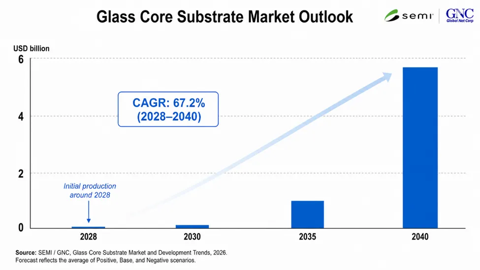
The report highlights increasing industry activity and investment around glass core substrates as companies prepare for the next phase of advanced packaging—providing an independent view of the technology’s market potential, development status, key players, and remaining barriers to commercialization. Under the report’s market-development scenarios, initial production could begin around 2028 in selected high-performance applications, with adoption expanding over time across larger and more complex package architectures. Based on the average of its Positive, Base, and Negative scenarios, the report projects a compound annual growth rate (CAGR) of 67.2% from 2028 to 2040. It also maps an increasingly active global development ecosystem, with companies and research organizations across Asia, North America and Europe advancing glass core substrate technologies.


Key topics covered in the report include:

  • Market outlook and adoption scenarios for glass core substrates 
  • Technology drivers and barriers to commercialization 
  • Expected applications in AI, HPC, advanced processors, co-packaged optics, and image sensors 
  • Company activities across substrates, glass materials, equipment, processing, inspection, and related supply-chain segments 
  • Development hubs, consortia, and supply-chain structure 
  • Forecast scenarios through 2040 

The Glass Core Substrate Market and Development Trends report is available in English and Japanese editions through SEMI Market Intelligence. Download the report.

For more information, please visit the Glass Core Substrate Market and Development Trends page or contact the SEMI Market Intelligence Team at [email protected].

Follow SEMI Market Intelligence

Follow SEMI 

About Global Net Corp.

Global Net Corp. is a Tokyo-based company serving the semiconductor and electronics industries. Established in 1990, the company provides wafer processing, equipment sales, consulting, technical seminars, research groups, and industry publishing services. Its technical and market coverage spans semiconductors, electronics, FPD, packaging, CMP, and related manufacturing processes.

About SEMI

SEMI® is the global industry association connecting over 4,000 companies and 1.5 million professionals worldwide across the semiconductor and electronics design and manufacturing supply chain. We accelerate member collaboration on solutions to top industry challenges through Advocacy, Workforce Development, Sustainability, Supply Chain Management and other programs. Our SEMICON® expositions and events, technology coalitions, standards and market intelligence help advance our members’ business growth and innovations in design, devices, equipment, materials, services and software, enabling smarter, faster, more secure electronics. Visit www.semi.org, contact a regional office, and connect with SEMI on LinkedIn and X to learn more.

Date: May 8, 2026

Location: Drammen, Norway

Board-level and semiconductor test data are often analyzed separately, limiting correlation across the product lifecycle. Linking PCB assembly (PCBA) test results, including in-circuit and functional test, with upstream wafer, sort, and final test data remains difficult, particularly in photonics, advanced packaging, and high-density integration environments. yieldWerx and WATS announce a partnership to bridge this gap in the PCB test and semiconductor manufacturing workflows.

WATS is a test data management platform purpose-built for electronics manufacturers. It captures, standardizes, and analyzes high-volume test data from PCBA (printed circuit board assembly) production environments, including in-circuit test (ICT), functional test, and final test, giving engineers real-time visibility into board-level yield, anomalies, and quality metrics across the production line.

yieldWerx operates at the semiconductor level, connecting data across wafer fabrication, wafer sort, die, and packaged device test. Its enterprise analytics platform enables advanced yield analysis, traceability, and root cause investigation from design through silicon manufacturing.

Together, the platforms address the full product stack. This allows manufacturers to correlate PCBA-level signals with silicon quality data, improving visibility across test stages and enabling more effective analysis of yield and reliability issues.

Customer and industry benefits include:

Real-time PCBA test visibility for faster identification of yield and quality issues

Improved correlation between board-level test results and upstream chip or wafer data

Reduced time spent reconciling data across disconnected systems

Earlier detection of cross-stage patterns impacting yield and reliability

Faster root cause analysis spanning silicon, assembly, and board-level test

Better alignment between electronics manufacturing and semiconductor supply chain

The combined solution supports open architectures, APIs, and flexible deployment models, enabling integration without large-scale system changes.

About yieldWerx

yieldWerx is an enterprise analytics platform connecting data across the semiconductor product lifecycle, from design and wafer fabrication through wafer sort, die, and packaged device test, enabling advanced yield analysis, traceability, and data-driven decision-making across cloud, on-premises, and hybrid environments.

About WATS

WATS is a test data management and analytics platform developed by Virinco, built to collect, standardize, and analyze data from electronics manufacturing test systems. It provides real-time visibility into board-level performance across ICT, functional test, and final test operations, helping engineers monitor yield, detect anomalies, and improve quality at high volume.

Statements from Leadership
"We are excited to partner with yieldWerx. Our customers manufacture complex electronics where board-level test data alone only tells part of the story. By connecting PCBA production test data with yieldWerx's upstream semiconductor intelligence, we can give them a more complete picture of their product quality and yield." -- Tom Lomsdalen, CEO, Wats

“Our customers have been asking for a unified view that links semiconductor yield data with downstream electronics test results, and this partnership delivers exactly that. Together, yieldWerx and WATS empower engineering teams to move faster on root cause analysis, reduce escapes, and make smarter decisions across the entire product lifecycle.” -- Aftkhar Aslam, CEO, yieldWerx

For further information, please visit https://www.yieldWerx.com or https://www.Wats.com/.

DRESDEN, Germany — May 6, 2026 — Global experts in advanced semiconductor packaging and 3D integration will convene at the annual SEMI 3D & Systems Summit, June 17–19, 2026, in Dresden, Germany. The Summit will deliver cutting-edge insights into the technologies and strategies shaping the future of heterogeneous systems and Europe's semiconductor ecosystem. Registration is open.

Themed Enabling Next-Gen Heterogeneous Systems Integration, this year's Summit will feature a program spanning geopolitical dynamics, market trends, AI hardware architectures, chiplet design, AR/VR and wearable intelligence, and the latest advancements in hybrid bonding and co-packaged optics.

“We look forward to welcoming industry leaders, innovators, and researchers to the 3D & Systems Summit 2026 in Dresden," said Laith Altimime, President of SEMI Europe. “As heterogeneous integration, chiplet architectures, and advanced packaging redefine system performance, the Summit provides a critical platform to align technology roadmaps, accelerate innovation, and strengthen Europe's position in next-generation semiconductor systems.”

3D & Systems Summit Sessions

Session 1: Market Trends and Europe's Technological Positioning

Executive leaders will examine the shifting geopolitical dynamics reshaping semiconductor supply chains, exploring industrial policy, regional fab strategies, and global benchmarking. Speakers will assess where Europe stands today and what is required to secure technology sovereignty across critical domains.

Session 2: Advanced Packaging Capacity: From Lab Innovation to Fab Deployment

Industry experts will address the full spectrum of advanced packaging, from fan-out technologies and outsourced semiconductor assembly and test (OSAT) strategies to supply chain considerations and lab-to-fab technology transfer. The session will highlight European strengths and the steps needed to scale advanced packaging capacity regionally.

Session 3: Hybrid Bonding: Die-to-Wafer & Wafer-to-Wafer

Specialists will examine hybrid bonding as a cornerstone of high-density 3D integration, covering die-to-wafer and wafer-to-wafer techniques, DRAM stacking, reliability engineering, and integration challenges across memory, logic, and advanced packaging.

Session 4: Photonics at Scale: Co-Packaged Optics

Industry leaders will explore co-packaged optics and photonic integration as key enablers of high-bandwidth communication, AI acceleration, and energy-efficient data movement, with discussions spanning optical interconnects, quantum photonics, and high-volume manufacturing readiness.

Session 5: Design Leadership: Chiplets & System Architecture

Experts will highlight chiplet architectures, CPU startups, and 3D integration strategy, showcasing the cutting-edge design activities that are positioning Europe as an emerging leader in system-level semiconductor architectures.

Session 6: AR/VR & Wearable Intelligence

Speakers will explore the convergence of optics, photonics, packaging, and efficient computing driving the next generation of AR/VR and spatial computing platforms, from displays and imagers to optical engines and low-power compute for consumer and industrial applications.

Global Leaders to Present

3D & Systems Summit presenters include experts from these global leaders

  • Adeia
  • ALLOS Semiconductors 
  • ams-OSRAM
  • ASML 
  • CEA-Leti
  • Confovis
  • Evatec
  • GlobalFoundries
  • imec
  • KLA 
  • Lam Research 
  • Murata
  • NXP Semiconductors 
  • STMicroelectronics
  • TechSearch International
  • Yole Group

Exhibition and Business Networking

The 3D & Systems Summit will feature an exclusive exhibition area showcasing industry leaders alongside innovative emerging companies, as well as business-to-business matchmaking and networking opportunities throughout the event.

The networking reception will take place at the Hilton Dresden Hotel on the first evening prior to the Summit. The networking dinner will be held aboard a historic paddle steamer on the Elbe River, following the final sessions of the first day.

Networking dinner registration is reserved exclusively for 3D & Systems Summit 2026 participants.

3D & Systems Summit Sponsors

Platinum: Adeia, ASE, Comet, Confovis, Lam Research

Gold: Evatec

Event: ASMPT, EV Group, imec, MKS Atotech

For more details, please visit the 3D & Systems Summit 2026 website and connect with SEMI Europe on LinkedIn or YouTube @SEMIEurope (#3DSummit).

Call for Abstracts Open for the 2026 Advanced Packaging Conference (APC) 

SEMI Europe has opened the call for abstracts for the 2026 Advanced Packaging Conference (APC), inviting industry leaders, researchers, and innovators to submit presentations highlighting the latest breakthroughs in advanced packaging, testing, and heterogeneous integration technologies. 

Themed Power and Interconnects Innovations Enabling AI System Performance, APC 2026 will explore how innovations such as 2.5D/3D integration, chiplet architectures, co-packaged optics, advanced materials, AI-driven design flows, and next-generation thermal and power management are enabling the future of AI, high-performance computing (HPC), automotive, and edge applications. Abstract submissions are open through July 1, 2026.

About SEMI 

SEMI® is the global industry association connecting over 4,000 companies and 1.5 million professionals worldwide across the semiconductor and electronics design and manufacturing supply chain. We accelerate member collaboration on solutions to top industry challenges through Advocacy, Workforce Development, Sustainability, Supply Chain Management and other programs. Our SEMICON® expositions and events, technology communities, standards and market intelligence help advance our members’ business growth and innovations in design, devices, equipment, materials, services and software, enabling smarter, faster, more secure electronics. Visit www.semi.org, contact a regional office, and connect with SEMI on LinkedIn and X to learn more.  

Date: April 21, 2026
Location: Hsinchu, Taiwan

yieldWerx is expanding its presence in Taiwan through a collaboration with Enlight Technology Co., Ltd., bringing advanced test data aggregation and analysis capabilities to one of the world’s most concentrated semiconductor markets.

The collaboration combines Enlight Technology’s established role across Taiwan’s semiconductor design, manufacturing, and research landscape with yieldWerx’s expertise in data aggregation and statistical analysis. Together, the companies aim to address the increasing demand for data-driven yield optimization as device complexity grows across advanced packaging, silicon photonics, and heterogeneous integration.

Enlight Technology is the authorized representative of Siemens EDA in Taiwan and provides a portfolio of electronic design automation (EDA), manufacturing execution systems (MES), and engineering solutions spanning IC, silicon photonics, MEMS, PCB, and system-level applications. The company supports semiconductor and electronics customers, including fabless design houses, foundries, OSATs, and system companies, with engagement across more than 100 semiconductor organizations and 300 system companies in the region.

As part of the partnership, the companies will work together to:

Provide localized technical engagement and support aligned with Taiwan’s semiconductor workflows and language requirements.

Support improved yield learning cycles and more efficient production ramp across the region.

Extend yield analytics capabilities into an ecosystem spanning design, verification, and manufacturing execution.

“We are excited to partner with Enlight Technology as we expand into Taiwan and the broader Asian market. Their deep domain expertise and strong ecosystem presence significantly enhance our ability to deliver scalable, data-driven yield solutions to customers operating at the forefront of semiconductor innovation.” — Aftkhar Aslam, CEO, yieldWerx

“As advanced packaging and silicon photonics drive exponential test data growth, our partnership with yieldWerx equips Taiwan's ecosystem with powerful statistical analysis. We empower customers to turn complex data into actionable insights, accelerating yield learning and time-to-market” — Su Cheng Yu, General Manager, Enlight Technology

About yieldWerx
yieldWerx is a leading data and yield analytics platform for semiconductor manufacturing, advanced packaging, and photonics I/O. The platform provides end-to-end visibility across wafer probe, optical and electrical wafer acceptance, module assembly, and system-level test. By analyzing this data, yieldWerx helps organizations understand yield performance, variability, and production trends, enabling optimized quality and faster time-to-market.

About Enlight Technology Co., Ltd.
Enlight Technology Co., Ltd. is a Taiwan-based provider of electronic design automation and engineering solutions and serves as the authorized representative of Siemens EDA in Taiwan. The company delivers solutions spanning IC, silicon photonics, MEMS, PCB, DFM, and manufacturing execution systems, supporting customers from IC-level design to system-level integration. With over three decades of experience, Enlight Technology provides customized solutions and technical services to the electronics industry.

For further information, please visit https://www.yieldWerx.com or https://www.enlight-tec.com/.