
downloadGroupGroupnoun_press release_995423_000000 copyGroupnoun_Feed_96767_000000Group 19noun_pictures_1817522_000000Member company iconResource item iconStore item iconGroup 19Group 19noun_Photo_2085192_000000 Copynoun_presentation_2096081_000000Group 19Group Copy 7noun_webinar_692730_000000Path
Skip to main content
Default Banner Image

Packaging

High-performance connectivity software delivers structured, high-volume equipment data required by tier-one fabs and advanced packaging facilities ahead of the expected mid-2026 SEMI standards update

POITIERS, March 25, 2026 – Agileo Automation, a leading provider of control and connectivity solutions for global semiconductor manufacturing, today unveils Agil'EDA, a new software solution implementing Equipment Data Acquisition (EDA), a set of SEMI standards also known as Interface A, to enable semiconductor equipment manufacturers to meet the evolving high-performance connectivity requirements of tier-one fabs and advanced packaging facilities.

As semiconductor manufacturing moves towards higher levels of automation and data-driven optimization, fab owners increasingly require EDA alongside traditional SECS/GEM connectivity from semiconductor OEMs for their production tools. Agil'EDA addresses this by separating the control flow from the data flow, ensuring that structured, high-frequency data collection does not interfere with critical equipment operations.
Designed for long-term deployment, Agil'EDA fully supports the widely used EDA Freeze 2 (SOAP/XML) and is architected for the transition to Freeze 3 (gRPC/protocol buffers). This next-generation standard offers significantly higher data throughput and reduced latency. Agileo has already successfully tested and validated its EDA Freeze 3 implementation at SEMI’s North America Standards Fall Meetings in November 2024 in Milpitas, California. SEMI’s EDA Freeze 3 standards suite is expected to be released mid-2026.

Complementing the SECS/GEM standards used to control equipment behavior, Agil’EDA incorporates robust cybersecurity features such as authentication and encrypted communications. The product is available as a stand-alone solution for any existing equipment software using a platform-independent gRPC application programming interface (API) to communicate with it or as a pre-integrated component within Agileo’s A²ECF-SEMI framework. When used with Agil'GEM and Agil'GEM300, it provides a comprehensive connectivity solution that significantly reduces time to market for OEMs.

"With the growing demand for data to improve yield in tier-one fabs, as well as in Advanced Packaging and 3D integration, EDA is no longer optional. It is becoming a mandatory requirement for equipment entering the world's most advanced fabs," explains Marc Engel, chief executive officer of Agileo Automation. "The key value we deliver for OEMs is a fast and easy adoption path for a seamless EDA architecture that delivers compliant production machines to global fab customers. By providing a future-proof architecture ready for Freeze 3, which will significantly increase performance, we address OEMs’ current needs while preparing them for the evolving requirements of semiconductor manufacturing, including AI-driven process control."

- ends -

About Agileo Automation
Agileo Automation is a trusted partner for equipment manufacturers, helping them build smarter, automated, and more connected machines that integrate seamlessly into advanced semiconductor fabs. Founded in 2010 in Poitiers, France, Agileo helps OEMs with control, communication, data acquisition, and testing across their tools through proven software and expert support. Its flagship A²ECF-SEMI framework provides a solid foundation for developing equipment controllers fully aligned with SEMI SECS/GEM, GEM300, and EDA standards. As an active member of SEMI and the OPC Foundation, Agileo Automation contributes directly to shaping the standards that drive manufacturing. For more information, please visit our website or follow us on LinkedIn.
Phoenix, AZ – February 18, 2026 – Plasmatreat USA, Inc., a subsidiary of Plasmatreat GmbH and a global leader in atmospheric pressure plasma systems and equipment, will showcase advanced solutions for particle-free, contactless, chemical-free, and inline-compatible surface pretreatment for semiconductor and electronics manufacturing at the IMAPS Device Packaging Conference, March 2–5, 2026, in Phoenix, Arizona.

As semiconductor devices continue to shrink while power densities increase, manufacturers face growing demands for surfaces that are exceptionally clean, oxide-free, and highly wettable to ensure reliable hybrid and chiplet bonding as well as wafer-level packaging. At the same time, flux residues, epoxy contamination, and oxide layers must be removed without chemicals while meeting stringent cleanroom requirements and maintaining consistent cycle times.

To address these challenges, Plasmatreat will present expanded plasma technologies designed to deliver low-particle, potential-free, dry surface preparation that integrates directly into inline production. These solutions enable both selective, localized treatment and uniform activation across large areas, resulting in stable interfaces, improved yields, and sustainable manufacturing processes without VOCs or aggressive chemical media.

Plasma Nozzle Technologies for Semiconductor Manufacturing

At IMAPS, Plasmatreat will highlight nozzle solutions based on Openair-Plasma® technology that support hybrid bonding, wafer-level packaging, and advanced semiconductor assembly.

The PDW100 dielectric barrier discharge (DBD) nozzle is a flat atmospheric plasma solution with a treatment width of up to 100 mm, enabling uniform activation across large, sensitive substrates. The system removes organic residues and oxide layers without generating particles, supporting high process stability and repeatability.

The PFA10 plasma nozzle delivers low-particle, potential-free plasma treatment for highly precise, localized surface preparation. The nozzle effectively removes organic contaminants and oxides while activating metallic and polymer surfaces, creating optimal conditions for hybrid bonding and chiplet stacking.

“With the expansion of our plasma nozzle portfolio, we are enabling new levels of purity and process reliability in semiconductor manufacturing,” said Hardev Grewal, President and CEO of Plasmatreat North America. “The PFA10 and PDW100 provide uniform, contamination-free surface treatment that is essential for reliable electrical and mechanical connections, even in ISO Class 1 cleanroom environments.”

HydroPlasma® Enables Advanced Residue and Oxide Removal

In addition to the nozzle technologies, Plasmatreat highlights HydroPlasma®, an advanced cleaning process that combines the physical effects of Openair-Plasma with the chemical reactivity of ionized water molecules to remove stubborn organic and inorganic contamination.

During the HydroPlasma® process, water is introduced into the plasma and ionized, creating highly reactive species that break down contaminants in a manner similar to detergent cleaning — but without chemical agents. The process is delivered through a precision jet, enabling targeted, non-abrasive cleaning of sensitive semiconductor components.

HydroPlasma® is particularly effective for removing epoxy residues commonly left on metal surfaces after die attach, underfill, encapsulation, potting, and rework processes. It also removes naturally occurring metal oxides that can degrade adhesion, electrical performance, and downstream process yields. The result is oxide- and residue-free surfaces that improve bonding reliability and overall manufacturing consistency.

The technology provides efficient removal of organic and inorganic contamination, including heavy oil residues, while remaining environmentally friendly, VOC-free, and safe for use on metal, glass, and polymer surfaces.

Plasmatreat’s Openair-Plasma® technology platform provides dry, chemical-free, and fully inline-capable surface treatment. The process reliably removes organic contaminants, silicones, and electrostatic dust while increasing surface energy to greater than 72 mN/m, supporting downstream processes such as die bonding, wire bonding, and underfill applications. Surface treatment is completed within seconds, delivers highly consistent results, and utilizes cost-effective process gases including compressed air or nitrogen.

New SECS-II library helps fabs and OEMs integrate semiconductor tools with the MES in hybrid manufacturing sites, ensuring faster time to market and limiting integration costs

MUNICH, November 18, 2025 – Agileo Automation, a leading provider of control and connectivity solutions for global semiconductor manufacturing, today unveils Agil’SECS-II at Booth #C2518 at SEMICON Europa 2025. This new SECS-II library, featuring built-in SEMI standard communication, enables a manufacturing execution system (MES) to accelerate the integration and validation of hybrid semiconductor and traditional manufacturing tools on production lines, ensuring faster time to market, lower integration costs, and reduced deployment risks. With this connection gateway, users can send and receive any SEMI SECS-II-compliant message as host or equipment for full GEM and GEM300 equipment integration and validation. This product can prove valuable for a variety of customers:

• Pure semiconductor original equipment manufacturers (OEMs) that need a practical way to develop an MES simulator and exercise their equipment under fab-like conditions. For small production lines or multi-tool set-ups exchanging data through SECS/GEM, Agil’SECS-II allows OEMs to design, test, and validate their equipment efficiently before shipping it to fabs.

• Customized, multi-industry, or low-volume production sites that use an MES system to integrate both traditional production machines and semiconductor tools. Agil’SECS-II simplifies integration in mixed equipment environments, especially where the MES cannot use SECS/GEM because most tools rely on protocols such as OPC UA, Modbus, or MQTT, yet semiconductor equipment using SECS/GEM must be integrated within the same MES.

• Laboratories and pilot lines without a full-featured MES that require a driver to collect data from various types of manufacturing equipment, including process, inspection, and metrology tools, to ensure quality and process control as well as complete traceability.

“With Agil’SECS-II, we wanted to provide a flexible tool that can serve multiple types of customers who can benefit from a proven software foundation built on more than 15 years of deployment experience in semiconductor fabs worldwide,” explains Marc Engel, chief executive officer of Agileo Automation. “Our SECS-II driver is especially useful for validating the processes of hybrid fabs that combine semiconductor and non-semiconductor manufacturing equipment, such as silicon carbide (SiC) wafer production lines or advanced packaging lines. It enables product and process traceability with legacy MES and helps OEMs developing equipment for these lines create MES simulators to verify information flow between tools using heterogeneous communication protocols.”

- ends -

About Agileo Automation
Agileo Automation is a trusted partner for equipment manufacturers, helping them build smarter, automated, and more connected machines that integrate seamlessly into advanced semiconductor fabs. Founded in 2010 in Poitiers, France, Agileo Automation helps OEMs optimize control, communication, data acquisition, and testing across their tools through proven software frameworks, applications, and expert support. Its flagship A²ECF-SEMI framework provides a solid foundation for developing equipment controllers fully aligned with SEMI SECS/GEM, GEM300, and EDA standards. As an active member of SEMI and the OPC Foundation, Agileo Automation contributes directly to shaping the standards that drive Industry 4.0 manufacturing. For more information, please visit our website or follow us on LinkedIn.

Nijmegen, October 20, 2025 – Chip Integration Technology Center (CITC) will become part of TNO. This strategic move marks a significant step toward ensuring the long-term continuity and stability of CITC’s research and operations. The integration emphasizes TNO’s ambition to take a leading position in the innovation of chip packaging technologies and strengthen the regional semiconductor ecosystem in Nijmegen.

“In the coming years, TNO aims to play a key role in the development of advanced chip packaging in the Netherlands,” says Arnaud de Jong, director of High Tech Industry at TNO. “By integrating CITC into TNO, we can intensify and expand our research efforts. We also contribute to the further development of Lifeport in Nijmegen as a strong, future-proof semiconductor ecosystem.” With the investment in CITC, TNO connects chip technology activities between Nijmegen and other semiconductor hubs such as Eindhoven.

Advanced chip packaging
CITC was founded in 2019 by TNO and Delft University of Technology (TU Delft), among others, as an independent innovation center for advanced chip packaging technology. Within an ecosystem of companies, research institutions and educational organizations, CITC has developed into a broad R&D hub that collaborates on technological breakthroughs in advanced chip packaging.

“CITC’s integration into TNO marks a noteworthy moment for CITC. This step underscores our shared vision for the future of chip integration and packaging technology,” says Jeroen van den Brand, general manager of CITC in Nijmegen. “This provides room for growth, accelerates innovation, and strengthens CITC’s international position as a center of expertise for chip packaging.”

Strategic choice for Nijmegen
CITC’s integration into TNO will formally take effect on January 1, 2026. CITC will become part of TNO’s High Tech Industry business unit and will remain located at the Noviotech Campus in Nijmegen. Toni Versluijs, chairman of the CITC Supervisory Board: “CITC continues on its current course. For the Supervisory Board, it is essential that, with TNO’s ambition and investment, we secure continuation of the CITC activities, while building on the existing talent and technology and give CITC room to grow further.”

Lucas van Vliet, member of the CITC Supervisory Board on behalf of TU Delft: “The collaboration between TU Delft and TNO within CITC will change form as of January 1 but remains as strong as ever. TU Delft believes in the importance and growth potential of chip packaging and sees incorporating CITC into a strong organization like TNO as an opportunity to further accelerate innovation in chip technology.”

- ENDS -

About CITC
CITC is a non-profit, joint innovation center specializing in heterogeneous integration and advanced chip packaging technology. With the aim of bridging the gap between academia and industry, CITC has created an effective ecosystem where companies, research and educational institutions collaborate. CITC was founded in 2019 with strategic partners TNO and Delft University of Technology and is supported by the province of Gelderland and Nijmegen municipality. Located on Noviotech Campus Nijmegen, CITC is perfectly situated in the heart of the Dutch semiconductor industry.
www.citc.org

About TNO
TNO is the largest independent research and technology organization in the Netherlands and one of the largest in the EU. We innovate, investigate, and orchestrate, collaborating closely with governments, universities and the private sector. We inform government on policies and empower evidence-based decision-making through rigorous investigations, cutting-edge scientific insights, and reliable measurements. By building national and international consortia and ecosystems, we drive technological and methodological breakthroughs that help to realise a secure, sustainable, healthy, and digital society, and strengthen the earning power of the Dutch economy.
www.tno.nl/en/

Contact
Christian Ketelaars, Communications Manager
E [email protected]
M +31 (0)6 48 15 42 92

Lam Research Introduces VECTOR® TEOS 3D to Address Critical Advanced Packaging Challenges in Chipmaking 

Inter-Die Gapfill Tool Expands Industry-Leading Portfolio of Solutions for 3D Integration and Chiplet Technologies; Paves Way for New, AI-Accelerating Architectures 

FREMONT, Calif., Sept. 9, 2025 -- Lam Research Corp. (Nasdaq: LRCX) today unveiled VECTOR® TEOS 3D, a breakthrough deposition tool engineered specifically for the advanced packaging of next-generation chips required for artificial intelligence (AI) and high-performance computing (HPC) applications. TEOS 3D is purpose-built to solve critical challenges in 3D stacking and high-density heterogeneous integration. It provides ultra-thick, uniform, inter-die gapfill, leveraging a proprietary bowed wafer handling approach, innovations in dielectric deposition, and enhanced monitoring by Lam Equipment Intelligence® technology. TEOS 3D is installed at leading logic and memory fabs around the world. 

"VECTOR TEOS 3D deposits the industry's thickest, void-free, inter-die gapfill films, customized to meet the challenging requirements of advanced die stacking integration schemes, even on ultra-stressed, high-bow wafers," said Sesha Varadarajan, senior vice president of the Global Products Group at Lam Research. "It's another powerful addition to our best-in-class advanced packaging portfolio, which delivers the differentiated, atomic-level innovations chipmakers need to scale beyond Moore's Law and into the AI era."

Addresses Manufacturing Pain Points

The explosive growth of AI is driving the need for new devices that can support increasingly data-intensive workloads. Chipmakers are turning to 3D advanced packaging to integrate multiple dies into chiplet architectures to enable AI compute. By bringing memory and processing closer together to optimize electrical pathways, chiplet designs can improve processing speed, and pack more power into smaller form factors. However, as chiplets scale taller and become more complex, they present a range of new manufacturing hurdles, from stress during processing that can distort or bow a wafer's shape, to cracks and voids in films that cause defects and lower yield. 

TEOS 3D conquers a range of critical advanced packaging production challenges, excelling at handling bulky, high-bow wafers precisely and reliably. With nanoscale precision, it deposits specialized dielectric films of up to 60 microns thick between dies, with scalability to deposit films greater than 100 microns. The films provide essential structural, thermal and mechanical support to prevent common packaging failures such as delamination. TEOS 3D also features Lam's novel clamping technology and an optimal pedestal design that provides exceptional stability when processing thick wafers, enabling uniform film deposition even when dealing with extreme wafer bow. 

Other highlights include: 

  • The first solution for single-pass processing of crack-free films more than 30 microns thick, significantly enhancing yield and process time.
  • Unique quad station module (QSM) architecture to boost productivity: Lam's proven QSM architecture features four distinct stations to enable parallel processing and reduce bottlenecks. The modular design helps deliver nearly 70%1 faster throughput and up to 20% improvement in cost of ownership compared to Lam's previous generation of gapfill solutions.
  • Lam Equipment Intelligence® technology for process repeatability: Built into TEOS 3D, Equipment Intelligence solutions boost equipment performance and reliability, and drive yield improvement by using smart technology to monitor processes, fix issues faster, and automate routine tasks.
  • Enhanced energy efficiency: Integrated high-efficiency RF generators and ECO Mode peripheral control reduce energy consumption while improving process precision. 

Joins an Industry-Leading Suite of Advanced Packaging Solutions 

Leveraging the company's 15 years of leadership in advanced packaging and decades of expertise in dielectric films, TEOS 3D builds on Lam's existing VECTOR® Core and TEOS product families, representing continuous innovation in materials and processes for integrated packaging. It is part of a comprehensive product portfolio of industry-leading solutions that addresses critical challenges and drives innovation and productivity across the advanced packaging workflow. 

Media Resources 

About Lam Research 

Lam Research Corporation is a global supplier of innovative wafer fabrication equipment and services to the semiconductor industry. Lam's equipment and services allow customers to build smaller and better performing devices. In fact, today, nearly every advanced chip is built with Lam technology. We combine superior systems engineering, technology leadership, and a strong values-based culture, with an unwavering commitment to our customers. Lam Research (Nasdaq: LRCX) is a FORTUNE 500® company headquartered in Fremont, Calif., with operations around the globe. Learn more at www.lamresearch.com. 

1 – Based on internal testing; 68%. 

Caution Regarding Forward-Looking Statements 

Statements made in this press release that are not of historical fact are forward-looking statements and are subject to the safe harbor provisions of the Private Securities Litigation Reform Act of 1995. Such forward-looking statements relate to, but are not limited to: industry trends, demands, expectations and requirements; the requirements of our customers; and the capabilities and performance of our products. Some factors that may affect these forward-looking statements include: business, economic, political and/or regulatory conditions in the consumer electronics industry, the semiconductor industry and the overall economy may deteriorate or change; the actions of our customers and competitors may be inconsistent with our expectations; trade regulations, export controls, tariffs, trade disputes, and other geopolitical tensions may inhibit our ability to sell our products; supply chain cost increases, tariffs and other inflationary pressures have impacted and may continue to impact our profitability; supply chain disruptions or manufacturing capacity constraints may limit our ability to manufacture and sell our products; and natural and human-caused disasters, disease outbreaks, war, terrorism, political or governmental unrest or instability, or other events beyond our control may impact our operations and revenue in affected areas; as well as the other risks and uncertainties that are described in the documents filed or furnished by us with the Securities and Exchange Commission, including specifically the Risk Factors described in our annual report on Form 10-K for the fiscal year ended June 29, 2025. These uncertainties and changes could materially affect the forward-looking statements and cause actual results to vary from expectations in a material way. The Company undertakes no obligation to update the information or statements made in this press release. 

Company Contacts: 

Allison L. Parker 

Media Relations 

(510) 572-9324 

[email protected] 

Ram Ganesh 

Investor Relations 

(510) 572-1615 

[email protected] 

Source: Lam Research Corporation, (Nasdaq: LRCX)


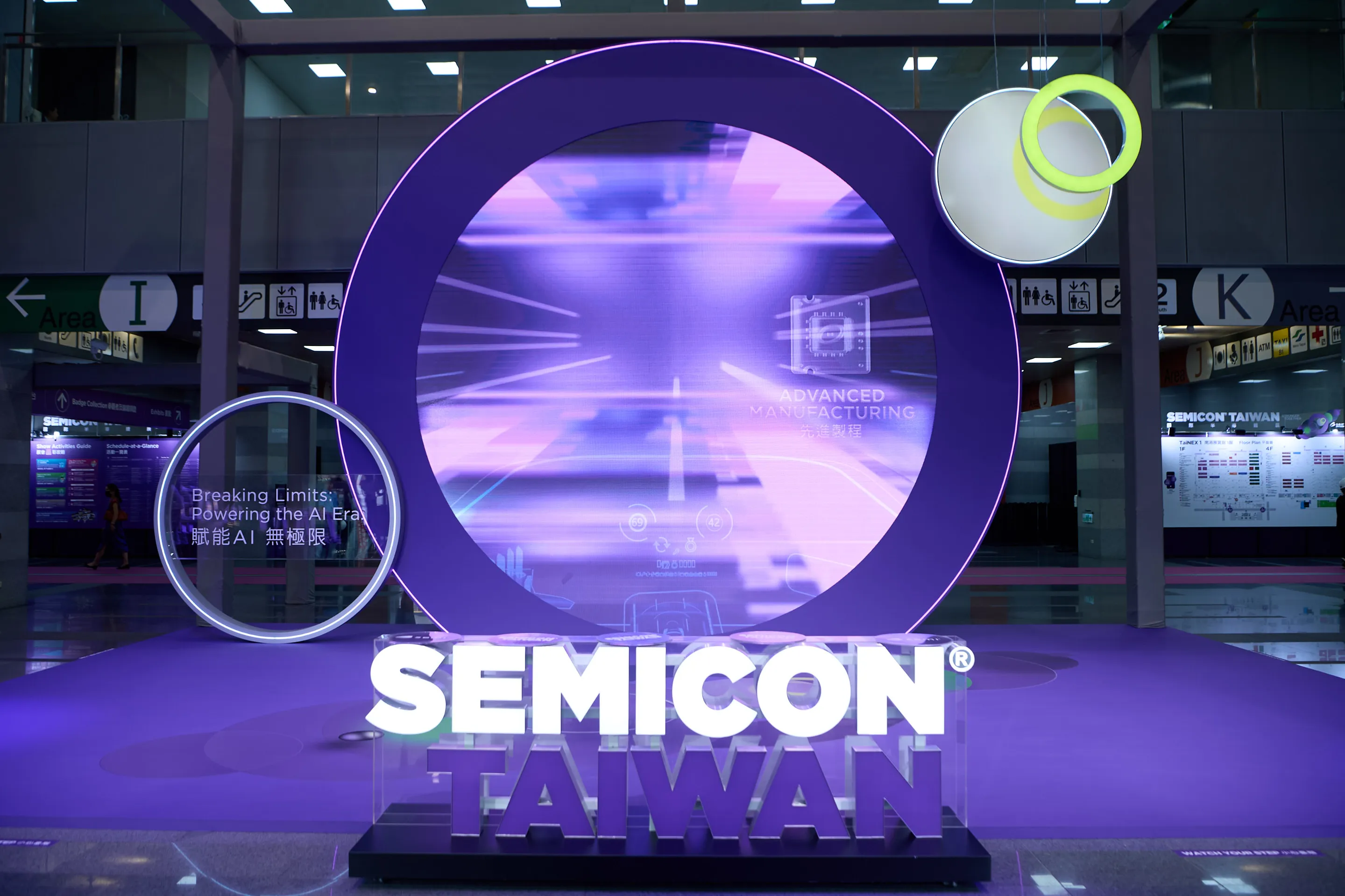
【Aug 28th, 2025 – Hsinchu】 SEMICON Taiwan 2025 is just two weeks away, and this year’s forums will welcome an extraordinary lineup of speakers. Silicon Valley “chip legend” Jim Keller will take the stage at the CEO Summit, while Dr. Chin-Tay Shih, a pioneering force in Taiwan’s semiconductor development, is confirmed to join the SEMI 20 Under 40 Awards Ceremony and Tech Master Forum. As the industry builds its central role in the AI era, global leaders will gather in Taipei to chart the future of semiconductor innovation.


▲SEMICON Taiwan Featuring Chip Guru Jim Keller and Industry Pioneer Dr. Chih-Tay Shih


Industry Legends Gather in Taiwan to Spotlight Innovation and Leadership

Tenstorrent CEO Jim Keller, renowned for his groundbreaking chip designs at Intel, Tesla, and AMD, will headline the CEO Summit with a keynote addressing the key technologies shaping the future of computing. A fireside chat focused on Taiwan’s strategic role in the global semiconductor landscape will follow, featuring co-moderators Dr. Tien Wu, CEO of ASE and Chair of the SEMI International Board Executive Committee, and Cliff Hou, Chairman of TSIA, along with panelists Jim Keller and Jochen Hanebeck, CEO of Infineon.

Also taking the stage, Dr. Chin-Tay Shih, a pioneering architect of Taiwan’s semiconductor rise, will reflect on his journey from ITRI to helping establish UMC, TSMC, and VIS, underscoring how Taiwan built a complete supply chain and laid the foundation for today’s AI era. Joining the Tech Masters Forum are Professor Y-W Peter Hong of NSTC, GC Hung, Senior VP of UMC, and Emily Hong, Chair and Chief Strategy Officer of Wiwynn Corporation.


Post-Moore Era: Heterogeneous Integration and Advanced Packaging Take Center Stage

With scaling reaching its limits, heterogeneous integration and advanced packaging have become the new frontier of innovation. SEMICON Taiwan will debut a dedicated Heterogeneous Integration Zone with nearly 60 companies. The zone includes the 3DIC Advanced Packaging Pavilion, Semiconductor Packaging Pavilion, and FOPLP Pavilion.

On September 9, the 3DIC Global Summit will bring together leaders from ASE, Chroma, GPTC, MediaTek and TSMC, to tackle key issues including efficiency, yield, cross-domain collaboration, and standardization. The day will also see the launch of the SEMI 3DIC Advanced Manufacturing Alliance (3DICAMA), rallying global industry leaders to drive collective innovation and propel advanced packaging into its next wave of breakthroughs.


Register now for SEMICON Taiwan 2025 to skip the lines. Industry professionals can get a free admission code by August 31. For more details visit the offical Website.


About SEMI

SEMI® is the global industry association connecting over 3,000 member companies and 1.5 million professionals worldwide across the semiconductor and electronics design and manufacturing supply chain. We accelerate member collaboration on solutions to top industry challenges through Advocacy, Workforce Development, Sustainability, Supply Chain Management, and other programs. Our SEMICON® expositions and events, technology communities, standards, and market intelligence help advance our members’ business growth and innovations in design, devices, equipment, materials, services, and software, enabling smarter, faster, more secure electronics. Visit  www.semi.org or join SEMI Facebook, and SEMI LinkedIn, and SEMI Official Line Account.
 

Test Research, Inc. (TRI), the leading test and inspection systems provider for the electronics manufacturing industry, will join SEMICON Taiwan held at Taipei Nangang Exhibition Center, Hall 1 – 1F from September 10 - 12, 2025. Visit TRI's Booth No. K3070 to learn more about the latest Advanced WLP/PLP and SEMI Back-End Package Inspection and metrology solutions.

TRI's Inspection and Metrology Applications include: Chiplet & Chip-on-Wafer (CoW), System-in-Package (SiP), Advanced WLP, TSV Metrology, μBump, Cu Pillar, Surface Topology, Profiling, Thin Film Thickness, Patterned Wafer, Inner Crack / Chipping, After Sawing Defects, Die Underfill, Glue, Epoxy & Flux, Wafer Bumping and Die / Wire Bonding.

TRI will showcase the Wafer Inspection and metrology Platform, TR7950Q SII, capable of wafer macroscopic 3D inspection and micro measurement metrology. The TR7950Q SII has applications in Advanced WLP, Wafer Frame, Patterned Wafer, Wafer Bumping, WLCSP, Through Silicon Via (TSV), thin film, and more.

TRI will also exhibit the back-end inspection solutions, the TR7007Q SII-S for C4 bumps (~100 μm Ø), Mini-LED, and 008004 paste inspection applications, and the TR7900Q SII-R TRI's Reject Station with A-Powered 3D Inspection that can inspect die, wire diameters of up to 15 μm (0.6 mil), SiP, underfill, bumps, and more. The lineup will also include an X-ray Inspection Demo Station. TRI's SEMI AXI solutions can inspect C4 bumps and Cu pillars.

Visit TRI's Booth No. K3070 at SEMICON Taiwan 2025 to explore TRI's SEMI solutions.

###
About TRI
Test Research, Inc. (TRI) offers the most robust product portfolio in the industry for Automatic Test and Inspection solutions. TRI provides the most cost-effective solutions to meet a comprehensive range of manufacturing Test and Inspection requirements. Learn more at http://www.tri.com.tw. For sales and service information, please write to us at [email protected] or call +886-2-2832 8918.

Lightium, MPI Corporation, and Axiomatic_AI Announce Strategic Partnership to Revolutionize Photonic Integrated Circuit (PIC) Device Testing with AI-Driven Solutions
Zurich, Switzerland; Hsinchu, Taiwan; and Boston, USA – January 6, 2025 – Lightium AG, MPI Corporation, and Axiomatic_AI Inc. have entered into a Memorandum of Understanding (MoU) to jointly develop the world's first Intelligent, Autonomous, and Integrated Test Solution (IAITS) for photonic devices.
This strategic collaboration aims to revolutionize the testing and qualification processes of photonic integrated circuit (PIC) devices by uniting state-of-the-art artificial intelligence, next-generation hardware, and deep domain expertise. The IAITS platform will deliver breakthrough performance in testing workflows—enabling unmatched efficiency, precision, and scalability to meet the ever-evolving demands of the photonics industry.
A Unified Vision for the Future of Photonics Testing
This partnership is driven by a shared commitment to deliver groundbreaking AI driven and self-optimizing solutions to the photonics industry. By combining Axiomatic_AI’s cutting-edge, reasoning-based, self-learning artificial intelligence with MPI Corporation’s industry-leading wafer probing systems and automation software, and leveraging Lightium AG’s advanced testing infrastructure and deep expertise in ultra-high-speed photonic device measurements, the collaboration aims to bring fully integrated, intelligent photonic integrated circuit (PIC) test solutions to market.
Together, the three companies are creating a unified AI platform that addresses the growing complexity and performance demands of characterizing photonic integrated circuits—unlocking new levels of automation, precision, and scalability for next-generation applications.
Disruptive Value Creation Across Hardware and Human Resources
The Intelligent, Autonomous, and Integrated Test Solution (IAITS) introduces a new paradigm in photonic integrated circuit (PIC) testing, delivering transformative value across both technology infrastructure and human capital.
Key Benefits of IAITS:
• Increased Throughput: By automating complex test routines, minimizing downtime, and optimizing measurement system utilization, IAITS significantly accelerates test cycles and reduces iteration times.
• Enhanced Human Efficiency: The system reduces reliance on manual operation, programming, and debugging—freeing skilled personnel to focus on high-value engineering and strategic innovation tasks.
IAITS will be commercially available as an advanced software add-on package for MPI Corporation’s wafer probing systems. Designed to support both R&D and high-volume production environments, the solution sets a new industry benchmark for efficiency, precision, and scalability—ultimately lowering the total cost of testing and accelerating time-to-market for next-generation PIC devices.
About Lightium AG
Lightium AG is a Swiss-based startup specializing in Photonic Integrated Circuit (PIC) foundry and design services, built on its proprietary, production-grade Thin-Film Lithium Niobate (TFLN) platform. Lightium accelerates customer innovation by delivering unmatched photonic performance, a streamlined and cost-efficient supply chain, and seamless scalability from prototyping to high-volume manufacturing.
As Europe’s first production-grade TFLN foundry, Lightium plays a pivotal role in enabling next-generation photonic solutions across a diverse range of industries, including telecommunications, data communications, quantum computing, artificial intelligence, and space technologies.
Further information can be found at: Lightium - Thin Film Lithium Niobate (TFLN) Photonic Foundry
About MPI Corporation
MPI Corporation, headquartered in Taiwan, is a global leader in advanced probe systems and testing solutions for the semiconductor, photonic, and photonic integrated circuit (PIC) industries. The company designs and manufactures high-performance wafer probing systems known for their exceptional precision, automation capabilities, and scalability—empowering cutting-edge testing across research, development, and high-volume production.
MPI’s innovations play a critical role in advancing next-generation technologies in wireless communication, electronics, and photonics. The company is publicly listed on the Taipei Exchange (TAIEX: 6223).
For more information, please visit: About MPI Corporation – Global Semiconductor Testing Leader
About Axiomatic_AI Inc.
Axiomatic_AI Inc., headquartered in Boston, is a pioneering startup developing physics-based reasoning artificial intelligence to accelerate innovation and reduce the cost and risk associated with deep-tech development. Its cutting-edge AI technologies are redefining how high-tech industries design, measure, and optimize complex systems—enabling faster, smarter decision-making across R&D and production environments.
Axiomatic_AI’s mission is to unlock new efficiencies and capabilities in fields where precision and complexity are paramount.
Learn more at: https://axiomatic-ai.com/mission/

This cutting-edge panel-level wet processing demo tool handles large 510 × 515 mm substrates, delivering world class, high density Through Glass Vias (TGV) formation and ultra-small taper angles essential for advanced packaging in high performance computing.

Gütenbach, Germany – July 15, 2025 – RENA Technologies, a leading manufacturer of wet processing equipment for semiconductor and advanced packaging production, today announced the ramp-up of its dedicated glass core substrates facility in Germany. This new line, designed for substrates up to 510 × 515 mm, immediately opens for customer test lots, underscoring RENA's proven expertise in glass processing and creating new opportunities for process development and customer sample production. “As experts in precision wet processing, we can now offer large panel demo services for high aspect ratio through glass via (TGV) formation on various glass types,” said Dr. Holger H. Kuehnlein, SVP Technology at RENA. “Our alkaline based TGV process delivers extremely small taper angles, low sidewall roughness, and exceptional dimensional control at panel scale, enabling high density via applications. Customers can begin validating these capabilities today.”

Why Glass, and Why Wet Processing?
Glass substrates offer significant advantages for advanced electronics, including ultra-flat surfaces, low dielectric loss, and superior thermal stability. However, realizing these benefits at scale requires defect free surface preparation and the formation of uniform, high density TGVs with minimal taper angles. RENA's wet processing systems are specifically designed to address both challenges:
1. Surface Engineering – Our systems ensure precise cleaning and stress relief across 600 x 600mm panels with submicron total thickness variation (TTV).
2. Chemically Formed TGVs – Following initial laser modifications performed by our specialist partners, RENA’s proprietary chemistries form, enlarge and shape each via to exact specifications. This process consistently delivers very small taper angles and smooth sidewalls, ideal for subsequent metallization.

By collaborating with leading German and international laser partners, RENA offers customers the flexibility to choose their preferred laser vendor while ensuring all downstream wet processing steps are handled by our advanced equipment.

Key Highlights of the New Facility
Panel Size: Focus on 510 x 515mm and up to 600 × 600mm, smaller possible
Tool Set: Alkaline TGV etching, advanced rinse/dry, optical inspection & metrology
Field-Proven Recipes: Process conditions migrated from high volume tools
On-Demand Access: Customers may run demo substrates, qualify custom chemistries, or request full process flows
Sustainability: Low temperature chemistries and closed loop water reclamation reduce energy and ultrapure water (UPW) consumption

Market Impact
High-Performance Computing (HPC) as well as 5G/6G RF modules increasingly require new package designs, including panel-level fan-out and trend towards more complex chiplet architectures. Glass substrates, long considered the “holy grail” for core and interposer material, effectively eliminate the limitations imposed by warpage and dielectric loss in organic substrates. By combining laser modification from our vetted partners with RENA's chemistry driven via shaping, designers can now validate glass packaging concepts on the lab-platform proven at 600x600mm dimensions.
“With this lab-tool, we've created a great opportunity for semiconductor manufacturers to perform demos on panel level glass substrates,” added Peter Schneidewind, CEO of RENA. “From surface preparation to via formation, our wet process flow is ready for customers substrates to support TGV technology breakthroughs. This is world class made in Black Forest.”

Availability & Engagement Model
• Testing available now
• Flexible collaboration: Bring your own laser modified substrates, or leverage RENA’s ecosystem partners to benefit from joint process development support, and metrology services for process validation.

About RENA Technologies GmbH
RENA Technologies is a leading global supplier of production machines for wet chemical surface preparation. RENA products are used in path-breaking application fields such as semiconductors, MedTech, renewable energies, the glass industry and additive manufacturing. RENA equipment is used to treat or modify surfaces of, for example, semiconductor wafers, solar cells, glass, optical substrates, 3D-printed metal components or other high-tech products using wet chemical processes. RENA offers proven standard machines as well as customer-specific solutions and process support.

CONTACT
Sales:
Felix Fink
Phone: +49 7723 9313-403
E-Mail: [email protected]

Press:
Dirk Hensel
Phone:+49 7723 9313-914
E-Mail: [email protected]
www.rena.com

Nordson Electronics Solutions, a global leader in reliable electronics manufacturing technologies, has developed several solutions for panel-level packaging (PLP) during semiconductor manufacturing. In one particular case, Nordson’s customer, Powertech Technology, Inc. (PTI) saw underfill yields improve to greater than 99% as they plan to transition from wafers to panels in their manufacturing operations. For details about this solution developed in late 2024 and 2025, download the case study here: Customer Success: Powertech Technology Inc. (PTI) Advances Panel Level Packaging with Nordson.

PTI, one of the world’s top OSAT (Outsourced Semiconductor Assembly and Test) companies, worked with the Nordson applications team to set up a comprehensive PLP demonstration that achieved high-quality, void-free underfill results at scale, using the industry-leading ASYMTEK Vantage® Series fluid dispensing system, equipped with the ASYMTEK IntelliJet® Jetting system. Nordson’s precision technology mitigated warpage and optimized fluid flow while decreasing cycle time by almost 30%.

PLP offers a path to managing the complexity of larger die sizes and higher-density designs while maintaining manufacturability and cost efficiency as the semiconductor industry transitions from 300-mm wafers to panels. PTI is enabling PLP applications that are designed to meet the semiconductor industry’s growing demands to serve AI, high-performance computing (HPC), and chiplet-based architectures.

Underfill has been pivotal in semiconductor packaging since the adoption of flip-chips in the 1990s. As applications have become more demanding, particularly in high-performance CPUs, GPUs, and advanced architectures like flip-chip and 2.5D/3D ICs, the importance of underfilling to enhance mechanical reliability and thermal performance has grown. Since the beginning, Nordson developed innovations for underfill processes as the industry evolved from PC board, substrate, wafer, and now panel applications.

Nordson’s distributor, Jetinn Global Equipment Ltd., supported the advancements discussed in this case study by investing in demonstration equipment and providing expert technical support.