downloadGroupGroupnoun_press release_995423_000000 copyGroupnoun_Feed_96767_000000Group 19noun_pictures_1817522_000000Member company iconResource item iconStore item iconGroup 19Group 19noun_Photo_2085192_000000 Copynoun_presentation_2096081_000000Group 19Group Copy 7noun_webinar_692730_000000Path
Skip to main content
Default Banner Image

Technology and Trends

AI vs. energy. Quantum for everyone. Biofabrication of human organs on a mass scale. Slowing advancements from Moore’s law.In the midst of a market dip, optimism reigned as keynote and AI Design Forum speakers addressed both looming challenges and explosive market opportunities during July 9-10 presentations at SEMICON West 2019 in San Francisco. SEMICON West again proved to be a magnet for visionaries who laid out the path to electronics innovation over the coming years.“The current business environment demands that the industry looks ahead toward issues that need attention sooner, not later – especially since we are approaching a once-in-a-generation inflection point that has the potential to be a $10 trillion opportunity,” observed SEMI Americas president Dave Anderson.Market forecasts punctuate the point: The microelectronics supply chain is on the verge of what has the potential to be the longest-lived electronics era.“Inflection points like this are rare, but not unprecedented,” Anderson added, citing 2007 as the inflection of the growth curve from new technologies that led to last year’s historic high semiconductor sales.SEMICON West squarely focused on the future, with a number of industry leaders noting that chip, tool and materials makers need to look beyond their immediate suppliers and customers in developing strategic partnerships. Dr. Cliff Young, data scientist with the Google Brain Team, for one, invited semiconductor and equipment firms to explore chip codesigning opportunities with his Google.The recently formed Quantum Economic Development Consortium – and its 50 members including Boeing, Google and IBM – debuted roadmapping activities devoted to the pursuit of U.S. leadership in the rapidly emerging global quantum computing industry. IBM’s Jeff Welser showcased the IBM Q Computer model built upon decades of semiconductor industry advances. Markets that could see staggering leaps from a quantum computational capacity include automotive, medical, financial and energy. Today, anyone can dabble with the future quantum computing capabilities by connecting online with IBM’s 16-qubit quantum computer. Dr. Aart de Geus, chairman and co-CEO of Synopsys, suggested that software and other programming tends to develop more quickly if it is open sourced. He recommends an open source model that allows semiconductor and equipment companies to work together in the cloud to speed chip development.Nate Baxter, TEL development and production group general manager, advocated sharing big data with competitors in pre-competitive spaces to ensure data quality, improve measurement and solve problems faster. The key is security. “Yes, we can share data while protecting it,” he said. “We’re quickly seeing opportunities that we didn’t know existed.”Gary Dickerson, Applied Materials president and CEO, said that embedding artificial intelligence (AI) in chips will drive significant long-term industry growth by processing far more big data computations much faster than humans can.That is, if there is enough electricity. Almost invisibly, AI-enabled machines already are crunching massive amounts of data while gulping power in the process. As AI use rapidly expands, current power grids will be stressed as never before. Dickerson added that speed of innovation, societal acceptance, security and safety will guide how well and quickly AI is adopted. A potential hurdle, however, is sustainability. He warned power constraints could be “very high” and a “barrier to AI adoption if we don’t drive innovation” in substantially reducing the power draw of power-hungry AI chips.Of the five members of a venture capitalist panel, four agreed that Moore’s Law as we knew it is dead. The promising news is that the average age of a first-time mobile phone user is 10, more than 40 percent of the world population is now under 25 and about to wield considerable market influence, and 5G is on the cusp of helping connect trillions of devices. AMD CEO Lisa Su noted “there’s a tremendous amount of innovation yet to come” from microarchitectural advances, chiplets and die stacking, and heterogenous platforms.And there’s nothing more innovative – or intriguing – than regenerating human organs in mass volume. Legendary inventor Dean Kamen laid out his well-funded plans to biofabricate the viscera of human existence but warned of two crucial missing pieces – scale and talent. “I’m here at SEMICON West to beg for high-tech’s help in getting artificial human organs out of labs and ramped up for volume manufacturing and widespread distribution,” Kamen said during his keynote. “The basic science already exists, but researchers can’t bring it to scale like Silicon Valley can.”The talent Kamen needs to fulfill his dream will come from the pool of skilled workers the microelectronics industry is feverishly working to recruit to make good on its own ambitions. As if on cue, SEMI endorsed Kamen’s FIRST Global program, establishing a united effort to encourage young people worldwide to pursue engineering careers. “Together, we can better help provide a path to success for generations to come,” SEMI’s Anderson said.Scott Stevens, SEMI
Read More
Renesas, one of the world’s very top MCU manufacturers, is heralding its new FD-SOI based R7F0E017 for energy harvesting applications. In an in-depth article in the May 2019 edition of EENews Embedded, Renesas Product Marketing Manager Graeme Clark detailed the new chip, which is sampling this year. It’s a fascinating read, with lots of explanations about how SOI enables the cutting-edge features (like an integrated energy harvesting controller) – you won’t want to miss it. BTW, here at ASN we’ve been covering the origins of this technology since 2005.They call it SOTB, for Silicon On Thin Box, but it is indeed their flavor of FD-SOI. The work started at Hitachi in cooperation with Renesas with a paper that debuted at IEDM 2004, then moved along through the series of mergers that resulted in the offering at what is Renesas Electronics today. Here are some key quotes from the article:“The new SOTB process can now offer active mode current of less than 20 µA/MHz and leakage currents down to 150 nA, while still allowing the development of devices with reasonably high clock rates, large embedded flash memories and SRAMs on chip. This combination of integration and power consumption will make devices developed on this process ideal for energy harvesting applications. The result of this new process is that we can develop a new generation of microcontroller products.” “The use of the Silicon on Thin Buried Oxide technology on this new device has resulted in some unique low power characteristics. The first device has the following features and future devices using this process could offer even lower power consumption. Active current of 20 µA /MHz Standby Current of 200 nAADC operation 3 µA @ 32 kHz256 Kbyte SRAM with 1 nA / Kbyte standby current” “The R7F0E017 is able to run safely from a pure energy harvesting power source due to the operation of the Energy Harvesting Controller. The device can operate from a wide range of potential energy sources including solar power, vibration, pressure and temperature difference, and many others. The integrated energy harvesting controller, supported by very few inexpensive external components, completely manages the cyclic wake-up sequence of the microcontroller, only using the extremely low energy harvesting source current.”Click here to read the full article on the eenewseurope website.
Read More
2019 will be a busy fall for the SOI Consortium and our members.First off are the SOI Consortium events in Shanghai and Tokyo, which are very popular indeed. We now have the dates locations locked in, so you’ll want to mark your calendars:Shanghai: 16 17 September 2019, FD-SOI Forum / RF-SOI Workshop. Both days will be held at the Pudong Shangri-La Hotel in Shanghai. The first day will focus on FD-SOI. The second day is all about 5G and RF-SOI. These are huge events – to get an idea of the magnitude, you can read our coverage of the 2018 event. Tokyo: 30 31 October 2019, Japan SOI Design Workshops. This year both days of workshops will take place in the Yokohama Landmark tower. The first day will be devoted to FD-SOI; the second day turns to More-Than-Moore – especially photonics and MEMS. Last year’s workshops were packed with excellent presentations and panel discussions, which we covered here. The SOI Consortium and members will also be giving talks at Semicon Europa, which is being held 13 – 15 November 2019 in Munich, Germany. The programs are currently being finalized. As soon as they’re ready, we’ll be sure to let you know so you can register and/or share the news with your colleagues and clients. But in the meantime, make sure you save the dates.Would you like to check out the presentations given at Consortium events in previous years? If you hover your cursor over the Events tab at the top of our home page, you’ll get a drop-down menu of events for the last five years (we’re working on adding more – we’ve been doing these events for over a decade!). Click through to any past event and you’ll land on a page where you can download most of the presentations that were given there. Of if you’re looking for past presentations given by any particular company, use the search engine at the bottom of any page on our website. S3SYou’ll also find many of our members at the IEEE/EDS S3S Conference in San Jose, CA, October 14 – 19th. S3S (formerly known as The SOI Conference) has been running in various forms for over 30 years. They always have an excellent line-up of speakers, plus it’s a great opportunity for networking with researchers from across the worldwide SOI ecosystem. BTW, while the deadline for general paper selection has already closed, papers of exceptional merit are currently being accepted for their Late News Sessions. See the 2019 Call for Papers for more information – those Late News papers need to be received by 23 August 2019 for consideration. Also, IEEE S3S Conference will once again host a full-day short course and a half day tutorial. These are very popular. The short course this year will be on SOI Design and Technology for Analog and Mixed Signal. As of this writing, the program is still being finalized, but more will be announced in the next few weeks, so check back on their website soon for updated information.Member EventsAnd finally, don’t forget to learn more about the offerings from and in support of the SOI ecosystem at our members’ events around the globe, including: GlobalFoundries – GTC | Samsung Foundry – SFF | ST – Technology Tour | Synopsys – SNUG | Cadence – CDNLive | Silvaco – SURGE | Arm – TechCon | NXP – Tech Days | Leti – Events | imec -Events |
Read More
This article is the first in a series highlighting the vital importance of SEMI Standards to commemorate the publication of the 1000th SEMI Standard in July 2019. Find the entire series here. More than 40 years after establishing the SEMI International Standards program, SEMI recently announced its 1000th SEMI Standard – a safety guideline for handling energetic materials. Creating a resource for unpredictable changes in materials is the type of challenge the SEMI International Standards program is often called upon to tackle – where the standard is merely the end of the beginning. The semiconductor industry has learned to expertly control its facilities, equipment and components. The next logical step is materials. It’s common knowledge that the industry drives innovation with new process materials and enabling safer material exploration is critical to the industry’s success. Classification Schema The 1000th SEMI Standard provides three classifications of energetic materials and byproducts based on three criteria: Hazardously exothermic (large amount of heat released following a trigger event such as heating or a physical shock) Pyrophoric (self-igniting upon air exposure) Water-reactive (releasing a large amount of energy or flammable gas upon contact with water) Unsafe handling of any of these byproducts can, to put it mildly, result in a bad day for a fab or lab. The leader of the Energetic Materials Task Force and an expert in process and equipment risk assessment at his company Safety Guru, Eric Sklar recounted one of the stranger incidents. A cleaning crew detached a pipe from a piece of equipment associated with a process recipe that used no energetic materials. The team set it in a sink, sprayed some water to begin cleaning it, and the pipe ignited in flames. Remarkably, although the initial materials weren’t energetic, the process created new byproducts that were very much so. Standardizing on Shifting Ground Energetic materials are new ground for standards and that ground is shifting, with much more material innovation to come. The upshot is that it is particularly important that the energetic materials standard is dynamic. By design, all SEMI Standards are malleable – continuously shaped by the demands they aim to meet. The release of this document is nowhere near the end of the work, as the standard will evolve to keep pace with continuing materials innovation. Creating a Robust Materials Supply Chain SEMI Standards create the conditions for a more robust materials supply chain and sustain the needs of business. If the standards safeguards are too burdensome, they will never be adopted. Conversely, without protections, people and equipment are unnecessarily put in harm’s way and innovation slows. SEMI’s Energetic Materials Task Force members realized early on that the industry needed a standard that would be practical to implement and flexible enough to be optimized over time. They understood that collaboration and compromise, while time-consuming, are also essential for standards’ creation. They determined roles and responsibilities across the supply chain, and they struck delicate balances between sharing no information about the intended uses of potentially dangerous materials and sharing everything about proprietary process recipes. The sheer scope of this standard necessitated a multi-year timeline. “The effort began with SEMATECH assembling its members’ views about energetic materials safety,” said Eric Sklar. “It then required years of effort from SEMI to bring the key industry participants together to create pragmatic guidelines that address the challenges around energetic materials in the supply chain.” Only Getting Started Despite all the work, one certainty is that the standard isn’t perfect for the present and can’t reflect future demands. This is why the energetic materials standard is not a static document, but a living process that is in its germinal stages. Key players continue to shape the standard, and that’s fundamental to enabling future materials innovation and ultimately reducing the number of unexpected energetic materials reactions in fabs. The variables in standards development are numerous and ever-changing. Energetic materials only magnifies the need for the broad collaboration that SEMI has facilitated for more than 40 years. While the risks posed by energetic materials are substantial, the criticality for continued innovation is undisputed. Now, with its adoption, the work of adapting and modifying this 1000th SEMI Standard is only about to begin. Use your voice to help drive standardization in and around the semiconductor industry. Learn about SEMI Standards – and become part of the solution. Register to receive Standards Watch, SEMI’s quarterly e-newsletter. Heidi Hoffman is senior director of technology communities marketing at SEMI. Hoffman and her team shine a spotlight on the work of the more than 20 technology communities under the SEMI electronics manufacturing supply chain collaboration platform. Actively engaging community members in marketing programs that showcase their unique value, Hoffman’s team helps companies grow and prosper through the power of connection, collaboration and innovation.
Read More
If you’re going to Semicon West this year, be sure to attend the SOI Consortium’s workshop on how IoT is driving the SOI supply chain. There’s a great line-up of speakers – see the program below. IoT means many things to many people but everyone agrees it’s here and growing quickly. IoT, including machine learning and movement to the edge, is fueling innovation as the high compute and ultra-low energy requirements are pushing technology to deliver on these needs. The well-known characteristics defining IoT of “Sense”, “Compute”, and “Act” put additional burden on technology to full these requirements across a variety of use cases and environments without sacrificing reliability or quality. All the various forms of SOI technology from FD-SOI to High-Voltage to RF-SOI, are uniquely situated to deliver on the promise of today’s as well as tomorrow’s IoT roadmap. The supply chain for all forms of SOI technology is in place. This workshop will discuss the current and future solutions from a supply chain perspective.Speakers include experts from SOI Consortium members Applied Materials, NXP, GlobalFoundries and Soitec.Entitled The Internet of Things, Driver of the SOI Supply Chain, the workshop will take place at the Moscone Center South, Wednesday July 10th in Room 301. It will run from 1 pm until 4:30 pm. Anyone and everyone who is registered for Semicon West is welcome. Here is the sign-up page.It’s a great program: 1:00pm - Welcome by Semi1:10pm - IoT/AI/Edge Market – Using SOI Through-out, Jon Cheek, Senior Director, NXP1:35pm - The SOI Opportunity, Manish Hemkar, Director, Semiconductor Products Group, Applied Materials2:00pm - The Foundry IP Ecosystem, Jamie Schaeffer, Sr. Director, GlobalFoundries2:25pm - Engineered Substrates - Enabling the IoT Revolutions, Eunseok Park, Director, Emerging Technology in Strategic Marketing, Soitec 2:50pm - Enabling the SOI Era, Thomas Uhrmann, Head of Business Development, EVG3:15pm - Panel: The Internet of Things, Driver of the SOI Supply Chain, Moderator: Carlos Mazure, Chairman, SOI Industry Consortium. Panelists include:Manish Hemkar, Director, AMATYoshio Kitahara, President Managing Director, Kokusai EuropeThomas Uhrmann, Head of Business Development, EVGJon Cheek, Sr. Director, NXPThomas Piliszczuk, EVP Strategy, SoitecJon Kretzschmar, Manager of Product Sales Marketing, TEL America4:05pm - Closing remarks, Carlos Mazure, Chairman, SOI Industry Consortium4:20pm - EndThis is a great chance to learn more about SOI and the SOI Consortium. Don’t miss it!And while you’re at West, you should also check out a related event. SOI Consortium member Leti will be teaming up with Fraunhofer for a workshop entitled New Paradigms in Microelectronics–Providing R D for the 21st Century. That happens at the nearby W Hotel in San Francisco on Tuesday, July 9th at 5:00pm. Click here for more information on that.
Read More
Post-Conference Report: SEMI Heterogeneous Integration SummitDemand for high-performance computing (HPC) chips is exploding. These super-speedy chips are critical for data centers and cloud computing infrastructures to support new performance-hungry technologies such as artificial intelligence (AI) and 5G. The challenge is for the devices and their multi-core architectures to couple high bandwidth density with low latency and high energy efficiency. Heterogenous integration offers a potential answer as an advanced packaging technology designed to meet these skyrocketing performance demands on HPC chips and open the door to a whole new world of 3D integrated circuits (ICs).So important are 3D ICs that Intel and TSMC representatives speaking at the recent Heterogeneous Integration Summit hosted by SEMI Taiwan in Taipei declared that the packaging technology will all but dictate the future of the industry. All told, 12 speakers from government, academia and a broad range of leading international companies from sectors including advanced packaging, design, manufacturing, silicon photonics, equipment and materials shared forward-looking strategies, the latest technologies and potential heterogeneous integration market opportunities. Koushik Banerjee, vice president, TMG, Assembly, and Test Technology Integration, at Intel pointed out that using heterogeneous integration for a single SiP (system-in-package) will deliver what the industry has long wanted by enabling multiple process nodes, more diverse silicon IP (intellectual property) and chip functionality, and chips that pair low energy with high frequency. Intel plans to announce its first Forveros 3D packaging product combining a 10nm HPC chiplet with a low-energy 22nm base die and stacked with memory on top. When asked about the future of advanced packaging technology, Banerjee said it will be very much about the combination of Foveros and its very own Embedded Multi-Die Interconnect Bridge (EMIB).For its part, TSMC, will continue to upgrade its CoWoS (Chip-on-Wafer-on-Substrate), InFO (Integrated Fan-out) and other 2.5D IC production solutions while developing 3D chip stacking technology such as SoIC and WoW (wafer-on-wafer). TSMC is ushering in a new age of 3D IC packaging, said Marvin Liao, Vice President, Backend Technology and Service Division, at TSMC. The company’s SoIC is based on Chip-on-Wafer concept, with the flexibility to support one-to-many or different process nodes, whereas its WoW integrates two wafers with solid yields that could be used for products of the same size or manufactured with mature process technology.Speakers also included representatives from ATOTECH, Lam Research, SPIL, Sigurd, Cadence, Grand Process Technology, ITRI (Industrial Technology Research Institute), Industrial Development Bureau, and Lee San-Liang, Distinguished Professor, Department of Electronic and Computer Engineering at National Taiwan University of Science and Technology all shared their perspectives on equipment, materials, and testing and how different industry value chains might contribute to the development of heterogeneous integration technology.Expected to be a key driver of the next wave of semiconductors, heterogeneous integration and related technologies – including 3D IC, FOWLP (Fan-out wafer-level packaging) / FOPLP (Fan-out panel-level packaging), silicon photonics, Micro LED, compound semiconductor, automated optical inspection and SLT (system level testing) – will be a key focus at SEMICON Taiwan 2019, September 18 to 20 in Taipei. The Heterogeneous Integration Innovation Zone – along with featured international programs such as SiP Global Summit, Strategic Materials Conference, the Smart Data Summit and the Smart Automotive Summit – will gather key industry players to reveal the latest technology breakthroughs and market trends.Emmy Yi is a senior marketing specialist at SEMI Taiwan.
Read More
New system-on-chip (SoC) devices are driving new memory architectures and photonic interfaces, while specialized new intellectual property (IP) requires analysis down to the nanometer and atomic levels because of single nanometer process nodes. According to Babak Taheri, CTO and EVP of products at Silvaco, a leading EDA Software, semiconductor IP company, a member of SEMI and the ESD Alliance, a SEMI Strategic Association Partner, design technology co-optimization and proven IP are required for this analysis.Taheri recently discussed atoms to systems in next-generation SoC designs with Nanette Collins ahead of ES Design West, co-located with SEMICON West, July 9-11 at the Moscone Center in San Francisco.ESD Alliance: For years now, the assumption is that each new chip design is more complex than the last. Why are the latest SoC designs even more complex than before?Taheri: New SoC devices for mobile phones, automobiles, intelligent edge nodes, big data compute and storage are adopting artificial intelligence and machine learning technologies. This is driving new compute, data flow, as well as memory architectures that are bandwidth-limited and some require photonic interfaces.One common denominator in present SoC design are the numerous blocks of IP. On average, over 85% of these blocks are reused. It’s cost-prohibitive to make these chips over and over again with new IP. According to some estimates, 90% of IP used in an SoC design by 2025 will be reused – only 10% is new technologies. That 10% is significant.ESD Alliance: How so?Taheri: Complex new technologies including flash memory, other advanced non-volatile memory technologies such as MRAM, RRAM and SoCs such as NVIDIA’s Xavier and Apple’s A12 use and reuse design IP at the architectural level.New technologies mean new materials and new processes. Single nanometer process nodes require specialized new IP that needs to be simulated and analyzed down to the nanometer and atomic levels.ESD Alliance: Does the atomic level changes the design equation?Taheri: Yes, it does. Designers need to be able to simulate at the atomic level and understand properties of these materials, and how they behave in at-process and at-device levels. They need be able to simulate the material's nanometer geometries, how molecules behave and how they interact for device operations. When they put together a process and a device, they need to know how the pieces behave and simulate before production.In other words, they run quite a few design experiments and quite a bit of simulation before they finalize the circuits and devices to silicon to save money.ESD Alliance: It’s obvious design automation will continue to have a vital role in design.Taheri: Yes, absolutely. Design technology co-optimization (DTCO) using TCAD solutions and proven design IP are needed to address the span from architecture to device and process physics. The importance of simulation, emulation and design technology co-optimization, along with fully verified and proven IP for SoC design, cannot be overstated. As designers generate devices and processors, they take that up to circuit-level simulation and high-level simulation, schematic capture, extractions and back annotation. They can go from atoms to simulating systems to the ability to do that under the same umbrella in order to get better chips, better yield and lower cost.Taheri’s talk Next Generation of SoC Design: From Atoms to Systems will be part of the Meet the Experts More than Moore session Tuesday, July 9, at 11:30 a.m. at the ES Design West SMART Design Pavilion. SEMICON West attendees are invited to Moscone Center’s South Hall to learn more about electronic system and semiconductor design and its links to the electronic product manufacturing and supply chain. Register for ES Design West or SEMICON West.Babak Taheri is Silvaco’s CTO and EVP of products, has more than 25 years of design experience. His current role managing Silvaco’s Technology CAD (TCAD), electronic design automation (EDA) and IP product divisions makes him an expert on what’s needed for the design of next-generation system-on-chips (SoCs). Previously, he was the CEO and president of IBT working with investors, private equity firms, and startups on M A, technology and business diligence. Babak received his Ph.D. in biomedical engineering from the University of California Davis with Bachelor of Science degrees in Electrical Engineering and Computer Science and Neurosciences. He has published more than 20 articles and holds 28 issued patents.Nanette Collins is a public relations representative for the Electronic System Design Alliance.
Read More
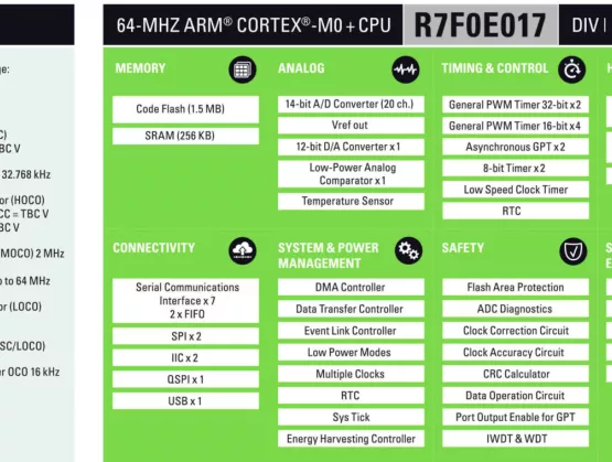
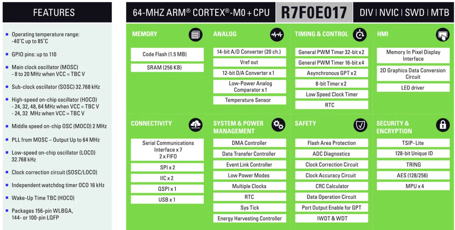
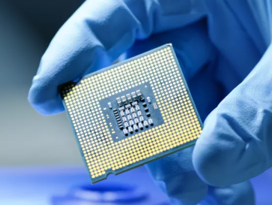
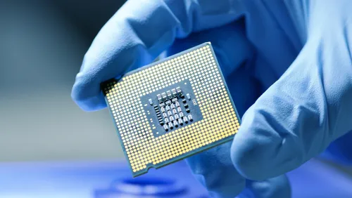
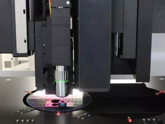
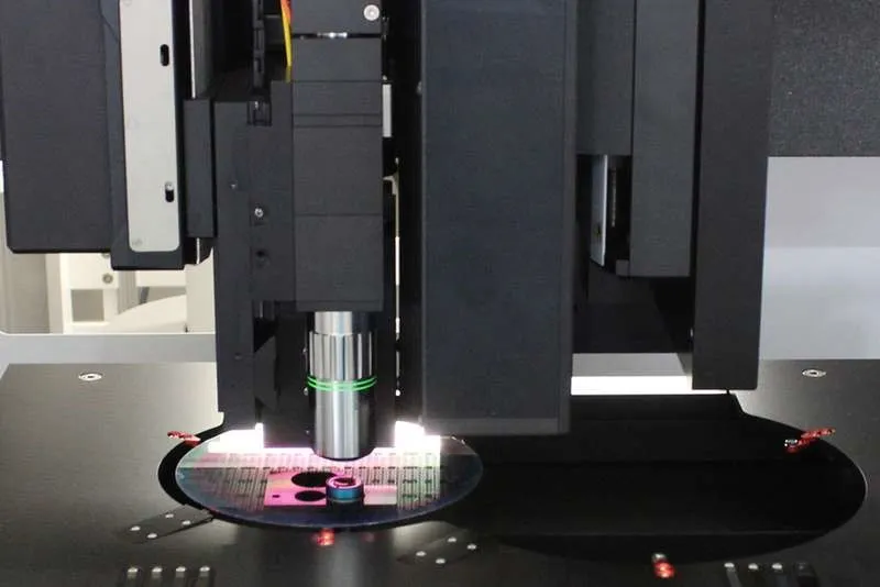
Shenyang is on an unwavering path to maturing its integrated circuit (IC) equipment manufacturing industry over the next few decades in response to the Made in China 2025 Strategy. Since the strategy’s introduction in 2015, the city, long a transportation and commercial hub of China's northeast, has built out a complete integrated circuit industrial chain integrating technical research and innovation, components and parts processing, and equipment manufacturing. Its ambition is to compete on the world stage.Shenyang has implemented policies and provided funding to support the development of its IC equipment and related industries to buttress the development of emerging industries. Speaking at the SEMI China Members Day 2019 in Shenyang, Zheng Guangwen, secretary-general of ICMTIA and Shenyang IC Equipment Industry Technology Innovation Strategic Alliance, said that the city, as a key IC equipment industry base in the upstream of China’s industrial chain, hopes to enter the international community in part by leveraging SEMI’s global platform. Zheng Guangwen, Secretary General, ICMTIA and Shenyang IC Equipment Industry Technology Innovation Strategic Alliance More than 150 representatives from member companies gathered at SEMI China Members Day 2019 to discuss China’s semiconductor industry investment and capital dynamics and semiconductor market trends. The event sought to promote stronger communication and interaction between the upstream and downstream of the semiconductor industry chain. The forum was co-sponsored by SEMI China and Shenyang Science and Technology Bureau and co-hosted by ICMTIA and Shenyang IC Equipment Industry Technology Innovation Strategic Alliance. Lung Chu, President of SEMI China Opening the event, Lung Chu, president of SEMI China, set stage for the discussion by noting that global semiconductor industry has been booming since 1957, reaching another record high of $470 billion in sales last year as it faced a critical juncture, with industry growth slowing in the first half of 2019. The slowdown was predictable and is temporary, a natural stage in the industry’s cyclicality. From a macro point of view, the development of advanced technology requires huge investment. There was an obvious gap in investment between enterprises, which often leads to the stronger become much stronger. Under these circumstances, it is very important for China to master key technologies and products during the process of catching up and surpassing. Each region should focus on its strengths.Enterprises should do their own business in a low-key way and keep a prudent and optimistic attitude. The number of SEMI China members has reached a new high. SEMI China is committed to becoming the best partner to realize China's semiconductor dreams. In promoting the development of global semiconductor industry and China's semiconductor industry, SEMI has continuously gathered strength and actively organized rich activities to promote the sustainable growth of Chinese semiconductor enterprises through international cooperation. Zhao Rigang, Director of SCTB, Shenyang Science and Technology Bureau Zhao Rigang, director of SCTB at Shenyang Science and Technology Bureau, pointed to the importance of SEMI’s pivotal role and global influence in cultivating cooperation between international and domestic industries including Shenyang’s IC sector. Speaking at the SEMI China Members Day 2019 in early June, Rigang said the growing importance of chips in China is a key catalyst for Shenyang’s rise as semiconductor sectors domestically and abroad invest heavily in a new generation of information technologies such as mobile Internet, cloud computing, big data, Internet of Things. Kang Jin, General Manager, SMIC Beijing For China’s semiconductor industry to flourish, the region must improve its IC supply capacity just as it has brought its PV industry to full maturation, said Kang Jin, general manager of SMIC Beijing. The key to developing China's integrated circuit industry, he said, lies in building a robust semiconductor supply chain. Zong Runfu, Chairman and General Manager, KINGSEMI Semiconductor Equipment Supply Chain DevelopmentLocalization has enabled KINGSEMI to optimize its technology design capabilities to produce high cost-performance equipment for greater competitive advantage, saidZong Runfu, chairman and general manager of KINGSEMI. While the localization rate of supply chain construction was over 50 percent, the localization rate for front-end equipment is still low. Zong Runfu said localization is imperative not only to lowering costs, but also to ameliorating the supply-guarantee rate, maintaining quality and shortening the delivery cycle. Russell Li, VP of Marketing and Business Development, WLCSP Packaging Solutions for 3D Active Sensing DevicesInternet of Things (IoT), artificial intelligence (AI), 5G and other technologies are starting to become a part of daily life as more sensors find their way into new retail stores and smartphones, a trend that will continue as autonomous transportation begins to take hold, said Russell Liu, VP of marketing and business development at WLCSP. The move to bring more human-like capabilities to technology is driving the implementation of perception function in devices, with passive sensors giving way to active sensors and machines translating the physical world into a 3D view through the eyes of a 3D camera. What’s more, the next generation of IoT devices will feature more integrated processors including signal processors, caches, sensors, photons, RF and MEMS, bringing the challenges of miniaturization to system integration. Liu said miniaturization will only be possible by developing advanced packaging technologies that enable highly integrated processors for mobile devices and intelligent automobiles. Wang Ronghua, VP of Technology, Dalian Xinguan Technology Getting Ready for GaN Power Electronics EraGaN offers excellent performance in optoelectronics, RF and power electronics and will coexist with and complement silicon devices for years to come, said Wang Ronghua, VP of Technology at Dalian Xinguan Technology. However, the industrialization of GaN power devices still faces technical challenges in application, reliability, packaging, epitaxy, device and process – all barriers to market adoption. To overcome these hurdles, GaN power devices must meet the reliability and cost-performance requirements of applications to which they are best suited.Ronghau said that GaN power devices, such as cascade and p-GaN enhanced devices, now support end products, proof that the era of gallium nitride has arrived. “Gallium nitride is quite different from silicon in epitaxy, device design and key technology, which requires close integration of upstream and downstream industry chains for effective promotion,” he said. Billy Feng, Executive Director, J.P. Morgan Is the Semiconductor Industry Still Cyclical? Since 2008, the semiconductor cycle has waned, disrupting the traditional thinking of investors, equipment suppliers and logistics channel providers as investors’ appetite for the chip industry investments has grown, said Billy Feng, executive director at J.P. Morgan. The long-term prospects for the semiconductor industry remain bright. But after reaching historic revenue highs in 2017 and 2018, the industry – and investor expectations – will enter a period of adjustment. Dr. Adam He, Executive Director, CGP Tech Fund The unique gene of the semiconductor industry consists of the blend of its lofty requirements for quality, reliability and consistency; cooperation between upstream and downstream sectors; internationalization; and a powerful ambition to innovate, said Dr. Adam He, Executive Director of CGP Tech Fund. He described Chinese chip enterprises he often encounters as falling into one of two entrepreneurial categories – IC experts and cross-border business people. Both want the answer to "how to make money and how to establish a solid competitive position?” He said. Adam believes that accessing the genes of the semiconductor industry is the answer to both questions and crucial to the maturation of China’s chip industry. The genes must be used to strengthen the Chinese manufacturing and materials sectors. Du Shanshan, Senior Analyst, SEMI China SEMI Market Outlook: Fab Investment, Equipment and Materials Market ForecastsEmerging technologies have sparked explosive semiconductor industry growth, said Du Shanshan, a senior analyst at SEMI China. While the industry will see a slight recession in 2019 due to memory market softness, trade wars and other factors, it is on stable footing for the long run. At the same time, China continues to optimize its IC industry chain, and semiconductor design and manufacturing companies have gradually grown in number. Over the next decade, the average growth rate of China's production capacity is expected to exceed 10 percent. Richard Feldman, VP of Global Expositions and Events, SEMI Richard Feldman, vice president of Global Expositions and Events of SEMI headquarters, presented the new SEMI Asia semiconductor business development plan to members and called on companies in mainland China, Taiwan and Malaysia to participate in SEMICON Europe to strengthen the influence of globalization.After the meeting, participants visited KINGSEMI Co., Ltd., Shenyang Piotech Co., Ltd, Shenyang SIASUN Robot and Automation Co., Ltd., Shenyang Fortune Precision Equipment Co., Ltd. and SKY Technology Development Co., Ltd. The event facilitated communications between upstream and downstream companies. SEMI China Member Day 2019 Group Photo Cherry Sun is a marketing manager at SEMI China.
Read More
SEMI spoke with Thomas Fries, founder and CEO of FRT GmbH, about how hybrid metrology is shaping multi-sensor metrology tools to enhance measurement precision as the industry moves away from a single-sensor approach.Fries offered his views ahead of the SEMI MEMS Imaging Sensors Summit, 25 to 27 September 2019 in Grenoble, France. Join us at the event to meet experts from FRT Metrology and many other MEMS, imaging and sensors companies. Registration is open. SEMI: Metrology in front-end used to be straightforward. But then, as the number of tasks to be implemented increased, we moved to a multi-sensors approach. What drove this transition?Fries: I believe it´s more about software than about sensors. But of course the basis is the hardware. So, most metrology tools were designed around a specific sensor, e.g. a white light interferometer.A rigid frame, wafer fixtures, scanning tables etc. were then added to develop a complete system. In manufacturing more machinery was added, like handling systems, cleanroom equipment and more sensors, mainly for additive functions such as reading IDs or measuring temperature. The center was still the one and only sensor, being pimped more and more by some hardware features and a lot of software.SEMI: How are sensors and software shaping the way metrology is applied today?Fries: Today a huge number of optical sensors are available to provide various measurement options. But sometimes there are only very slight differences from one sensor to the other. A tiny variation may determine whether we solve a problem or end up fishing in troubled waters.And of course using different machines with those sensors requires high budgets for capital investment, used floor space, measuring time, etc. A multi-sensor platform solves all these problems. But again, it is the software that makes the real difference.SEMI: What lead to those advancements in metrology? What problems did they set out to solve?Fries: Metrology has been evolving ever since the measurement standards were established. The first challenge was to create a flexible mechanical platform that was also reliable and stable. All components were designed to be integrated into one system, mechanically, electrically and of course in the software.This level of integration requires not only an appropriate user interface, but also data formats and evaluation algorithms that leverage multi-sensor hardware. Today every metrology tool in the fab is justified by the application, not by specific sensors or specs. Of course the application leads to a set of specs, but the solution for the metrology task is realized within the software.New developments in metrology combine expertise in system design, physical knowledge in metrology and materials, mechanical engineering and also mathematical and software skills.The last step was the implementation of hybrid metrology functionality into a multi-sensor system that opens totally new doors in metrology. Before multi-sensors development, quite a few hitches could not be properly solved. SEMI: This is especially true when we consider applications in advanced packaging and MEMS manufacturing. What is in your opinion the main challenge?Fries: Specifically, in MEMS and advanced packaging we face multiple metrology challenges, as various processes run in one step and conditions on the wafer may vary quite often. In this case, a high degree of flexibility, up to the option to upgrade the metrology tool at any time or place, is a priceless advantage. Besides, cost effects for footprint, throughput and investment play a key role.A central task for nearly every customer application is to combine global measurements (complete wafer) and local measurements (per die) within one recipe. This is a perfect case for a multi-sensor platform. Measuring step heights and film thickness in one take is also an everyday routine. Combining those characteristics to measure hidden structures (hybrid metrology) is unique.SEMI: How will hybrid metrology enhance measurement precision and where do you expect the multi-sensor approach to be more applicable?Fries: The first advantage is the ability to measure properties that you cannot access directly. On top of that, all the previously mentioned features such as facing multiple metrology tasks, the combination of complete wafer and per die measurement are playing key roles. The precision of specific measuring tasks can be optimized by calibrating sensors against each other or combining results to get rid of noise or artefacts.MEMS and advanced packaging are natural playgrounds for hybrid metrology. But already today we see applications in high volume manufacturing in the 300mm fabs. As structures on wafers shrink, wafers are getting thinner and the whole process is becoming more and more complex. The classic one-sensor metrology tool is running out of gas. SEMI: What are your expectations regarding the summit in Grenoble, and for the future of the MEMS Sensors technology?Fries: FRT has always been very strong in MEMS and sensors and we have attended and exhibited at the SEMI MEMS Imaging Sensors Summit from the very beginning. The summit is always a very good meeting point for the community, and a perfect training session that gives participants extended updates in all fields. And of course, it grows our network and gives us the opportunity to show our latest products and applications.If you really want to know how the future of MEMS and sensors will look like, join the summit and don´t miss the chance to pass by the exhibition to meet FRT and many other industry leaders.Dr. Thomas Fries lives with his family close to Cologne. He is engaged in a variety of activities: as technical advisor to various ministries, supervisory board of PlanOptik AG, board and advisory board of IVAM, board member of COPT.NRW e. V., just to name a few. FRT supports many social projects as well as kindergartens and schools. Motorcycles and cars are still a great passion alongside his family.Serena Brischetto is senior marketing and communications manager at SEMI Europe.
Read More
According to market research and strategy consulting firm Yole Développement (Yole), the total market size of MEMS, sensors and actuators will double from $48 billion in 2018 to $93 billion in 2024.[i] The consumer market will continue to drive volume, with applications such as smartphones making up for in volume what they lack in average selling price (ASP). Stronger demand in automotive, biomedical/health, industrial, and voice-first applications (such as smart speakers) will support this upward trajectory. With so much growth ahead of us, how will the design and manufacture of MEMS keep pace with industry demand for higher levels of innovation and integration, lower cost and lower power, smaller footprints, and faster design cycles — all while meeting acceptable price points?We turned to a handful of MEMS manufacturing experts from SEMI-MSIG who will join us at SEMICON West 2019, July 9-11 at the Moscone Center in San Francisco, to explore the complexities of keeping pace with market demand for MEMS over the next decade.Address the Design GapMentor GM, ICDS Division Greg Lebsack and SoftMEMS President Mary Ann Maher see tremendous progress in the manufacturing supply chain for MEMS. At the same time, they acknowledge the significant gap that still exists in design capability for creating the billions of interconnected sensors required for future applications. Greg and Mary Ann will dive into the standards, ecosystem requirements and collaborative design solutions that will allow the micro-sensors industry to meet demand for next-generation wearables, Internet of Things (IoT) products and medical devices.Get Collaborative with Greg and Mary Ann: Addressing the Design Gap to Enable Next Generation Sensor-Based Products, SEMICON West, TechTALKS South, Thursday, July 11, 2019, 10:35-11:00 a.m. Register today.Get to a Really Big NumberFrom thousands of sensors and actuators in a single airplane to hundreds in a single car or a piece of factory equipment to the twenty-plus that ship in each of the hundreds of millions of the world’s smartphones, we aren’t even close to reaching the saturation point for these intelligent devices. SPTS Technologies EVP GM David Butler isn’t living on the Spaceship Enterprise (or the Millenium Falcon, come to think of it) when he says that we are going to get to a trillion sensors. It is going to happen. The questions are: how and when?Connect with David: Enabling the Age of a Trillion Sensors, SEMICON West, TechTALKS South, Thursday, July 11, 2019, 11:00-11:25 a.m. Register today.Shift to Automotive-GradeDemand for optical sensing technologies such as LIDAR is shifting sensor manufacturing requirements from consumer- to automotive-grade, with its enhanced lifetimes, temperature cycling and higher performance specifications. To meet demand, manufacturers are turning to wafer-level processing, since it complies with the hermetic sealing and dew-point control required for the more rigorous automotive-grade applications. EV Group Business Development Director Thomas Uhrmann, Ph.D., will provide an overview of the steps for manufacturing optical elements, including integration with CMOS circuitry, as he offers a window into the future of automotive packaging for sensors.Tune in with Thomas: Future Manufacturing Requirements for Automotive and Photonics Sensing, SEMICON West, TechTALKS South, Thursday, July 11, 2019, 11:25-11:50 a.m. Register today. Measure Twice, Cut OnceFaster time-to-market, improved device yield, and greater productivity in high-volume manufacturing are increasingly critical requirements for MEMS manufacturers. When a single manufacturing error can cost hundreds of thousands if not a million or more dollars — as well as months of development time — designers can save both time and cost by employing an integrated approach to MEMS design. Lam Research Sr. Director of Strategic Marketing David Haynes will explain how simulation, verification and process modeling can address MEMS-specific engineering challenges such as multi-physics interactions, process variations, MEMS + IC integration, and MEMS + package interaction. Using the right tools before committing to actual fabrication can make or break a project.Get Conceptual (and Practical) with David: Enabling Better MEMS from Concept to High-Volume Production, SEMICON West, TechTALKS South, Thursday, July 11, 2019, 11:50 a.m.-12:15 p.m. Register today.Navigate a Dynamic Foundry LandscapeWe’re still living in a one product-one process world when it comes to MEMS manufacturing. This makes bringing a new device to market both time-consuming and expensive. These challenges aside, the functional capabilities of MEMS, combined with small-footprint and low-power options, have made MEMS increasingly popular. How are market dynamics in MEMS manufacturing evolving to accommodate both demand for high-volume, lower-cost products such as MEMS microphones as well as high-value, lower-volume products such as biomedical devices, IoT products and industrial sensors? Rogue Valley Microdevices Founder CEO Jessica Gomez will explain how foundry consolidation through acquisition, collaboration with other ecosystem players, and specialization in vertical markets such as biomedical or optical are some of the approaches that are transforming the MEMS foundry landscape.Join the Evolution with Jessica: Consolidation, Collaboration, Specialization: How Will MEMS Fabs Manage Changing Dynamics, TechTALKS Stage South, Thursday, July 11, 2019, 12:15-12:40 p.m. Register today.i“Status of the MEMS Industry report,” Yole Développement (Yole), 2019 Edition.Maria Vetrano is a public relations consultant at SEMI.
Read More