downloadGroupGroupnoun_press release_995423_000000 copyGroupnoun_Feed_96767_000000Group 19noun_pictures_1817522_000000Member company iconResource item iconStore item iconGroup 19Group 19noun_Photo_2085192_000000 Copynoun_presentation_2096081_000000Group 19Group Copy 7noun_webinar_692730_000000Path
Skip to main content
Default Banner Image

Technology and Trends

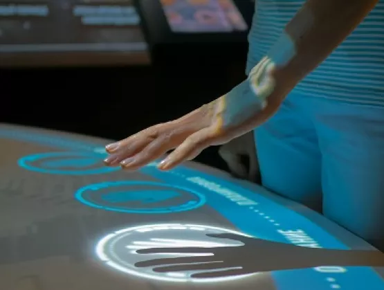
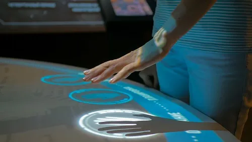
Olivier Corvez, senior manager of Environment, Health, Safety and Sustainability at SEMI, sat down (virtually) with Todd Patterson, vice president of global EHS for Entegris Global Operations, to discuss how Entegris has responded to the global pandemic.Corvez manages and Patterson participates in the COVID-19 EHS Task Force currently meeting weekly to discuss industry response and share best practices. SEMI: Was Entegris prepared for the COVID-19 pandemic? How did the company respond?Patterson: Entegris has a strong risk management framework and a risk assessment team of senior leaders who meet at least once a quarter. This focus gives us early visibility into events that could destabilize our organization or threaten our operations. Such a framework helps ensure we have the information necessary to act as soon as possible when the need arises. However, our business continuity plans for a pandemic of this scale were far less than with other more commonly occurring catastrophic events such as earthquakes or hurricanes. The COVID-19 crisis was clearly unprecedented and as such, the necessary systems and procedures were not in place with the depth and detail needed. Our strong governance structure made it possible for us to hold steady even as the pandemic caused increasing uncertainty and disruption around the world. For example, despite major supply chain shutdowns across many industries, to date, our supply chain and manufacturing operations have only been modestly impacted by COVID-19. Our supply chain team was assessing daily the areas of risk with our suppliers and taking appropriate action as well as preemptive steps to ensure our critical supply lines remained open.Our sales team engaged in regular communications with our customers providing them updates about our Business Continuity Plans and our actions to mitigate the risk to any of their deliveries. In addition, we maintained current information about the continuity of our supply chain on the company’s intranet for the global sales team to access as they engaged with customers. Also, a proactive communication plan was implemented immediately to send weekly video messages from senior executives directly to employees’ emails. It was an effective way to communicate with our global teams, to keep them informed about the status of the company’s operations and maintain a common sense of purpose at a time when many colleagues worked from home. In these weekly messages, we also focused significant attention on the health and safety protocols established to protect our manufacturing and lab employees from the virus.Among the health and safety protocols we implemented immediately as the virus moved across different regions were those related to facility screenings, work-from-home policies, social distancing, self-quarantine requirements, contact tracing, increased disinfecting, and travel restrictions. With approximately 5,300 employees worldwide, we had teams in every region ready to implement these comprehensive protocols. We believe we were among the first companies to implement work-from-home policies and travel restrictions.Temperature screening stations at Entegris facilities in Jangan, Korea (left) and Kulim, Malaysia (right). In addition, our CEO led a COVID-19 Steering Committee comprised of senior executives and managers from operations, human resources and communications. The committee met several times a week during March and April to evaluate and formulate responses to the issues that emerged as the virus spread from region to region. The committee’s work created a strong partnership among senior executives and divisional and functional leaders, and the initial guidelines developed by the committee have formed the backbone of a global playbook to limit the spread of the virus to our other sites around the world.Recently, the committee has changed its focus to more strategic issues such as creating a framework for transitioning remote workers back into our office locations. Meanwhile, local leadership teams at each of our global sites have been empowered to address ongoing tactical issues consistent with our thoroughly documented health and safety protocols.Looking to the future, we are using our experience in responding to COVID-19 to develop a more comprehensive pandemic response plan. We have project teams working on better ways to: measure temperatures of personnel entering our sites facilitate social distancing in the workplace redesign common use areas to reduce the number of high touch points disinfect all spaces thoroughly and regularly, and manage emergency pandemic supplies. SEMI: From the SEMI EHS survey, we noted that all members had a Business Continuity Plan. How effective has it been for deploying resources and adapting quickly and minimizing the crisis? Why or why not? Patterson: Because we have operations in China, Entegris experienced the impact of the virus immediately. We quickly formed two task force teams for our two primary facilities in the region. These teams developed the means for communicating key information to employees and started working on prevention plans to protect employees and comply with local requirements for when operations resumed. They met the challenges head on and found quick solutions. An example was finding an effective way of communicating to the employees for each location. Group chats were established through social media. It was this work that led to their success in getting approvals from local authorities to resume operations. Those plans have laid the groundwork on which our other sites around the world could build their response plans.The effective management of our global supply chain also stands out as a key success of the company’s Business Continuity Plan. Entegris has a highly complex supply chain with approximately 6,500 suppliers and a $850 million annual spend, and we ship work-in-progress and finished goods from over 90 sites globally.As I mentioned earlier, despite the virus crippling supply chains across many industries, Entegris experienced very little disruption to its supply chain. The supply chain team was able to accomplish this despite a 90% reduction in global freight capacity. A key factor in keeping goods flowing to our factories was the intensive work the team had done earlier to develop an in-depth understanding of the company’s top suppliers and to mitigate sourcing risks. They had established alternate sources, balanced the sources geographically, and placed inventory across our supply chain to buffer risk.The team also had integrated statistical modeling into reporting tools, which made it possible to reset safety stocks and logistics lead times quickly as conditions changed. And a supply chain digitalization provided one aligned and integrated view via dashboards, giving the company the ability to respond rapidly and to communicate in real time with our suppliers. We essentially had a virtual war room where we monitored the daily impact of the spread of the virus and could address bottlenecks and other issues immediately.SEMI: What lessons have been learned, so far? How do you see changes in your company’s operations in the future?Patterson: Institutionalizing what we’ve learned has already begun. Whether the measures implemented during the pandemic are temporary or become permanent is still to be determined. Regardless, the learnings need to be documented and available as a playbook for if – or when – the next pandemic occurs.Entegris is already working on a more comprehensive pandemic plan that will be based on five levels of preparedness. Level 0 will cover annual training requirements and management of emergency inventory of pandemic supplies. Level 1 will include early recognition of an outbreak, and then Levels 2-4 will include requirements for when specific response measures are implemented. Entegris also has formed the “New Normal” task force, which consists of leaders representing a number of disciplines directing the project teams previously mentioned to create a more comprehensive pandemic response plan. One of the project teams is working on improving the facility screening process that performs temperature measurement for personnel entering Entegris sites. The team is looking at the best technology to scan body temperature. As to whether this technology is employed only while COVID-19 is still active or becomes a permanent way of doing business, this is still being discussed.SEMI: EHS is involved in both providing technical support to protect individuals but also in making organizational changes to favorize social distancing. Could you explain some of the successes and challenges while tackling these two fronts?Patterson: Very early in the pandemic, Entegris established a work-from-home policy for non-essential employees. This significantly reduced the number of personnel and the potential for contact at the Entegris locations. Significant facility changes also were required. These included the design of facility screening booths and modifications to common gathering areas such as canteens, meeting rooms, prayer rooms, and smoking points. Physical markings were used to designate 2 meters distancing, and the seating in canteens and meeting rooms was reduced and staggered to minimize the risk of exposure to the virus. Entegris also has a project team focused on developing design solutions for offices and workstations when space makes it difficult to maintain 2 meters social distancing. These changes turned out to be essential for some sites in meeting mandates by local authorities. Our sites in Hangzhou, China and Kulim, Malaysia both were allowed to resume partial operations after demonstrating to government authorities the effectiveness of the preventative measures put in place. One particular challenge we are facing is the range of personal differences and awareness levels within the workforce – including those that don’t understand the importance of the new guidelines. We are working closely in advising supervisory staff to be aware of the need for employees to follow all health and safety protocols we have put in place, including social distancing. That preventative measure is the most difficult to make part of our new behavior – it is unnatural and inconsistent with our human nature, but it is critical to preventing the further spread of the virus.SEMI: How do you envision the progressive steps in deescalating to bring back “normal” operations? Patterson: I don’t know whether Entegris will ever go back to the old “normal.” As previously mentioned, we are working on the “New Normal.” Our focus now is on bringing our work-from-home employees back to the workplace without adding risk of exposure to the virus. We are still exploring options, but we expect to do it in a phased approach so that we can adequately assess the preventive measures that are in place and determine whether adjustments need to be made to any of our health and safety protocols.We are starting to see a variety of different frameworks emerge for evaluating repopulation timing and procedures. We will assess them on an office-by-office, or site-by-site basis, utilizing consistent criteria to define the potential for exposure to the virus. This also applies to our field service workforce. However, I have not yet seen any governmental guidance that offers a recommended framework for returning employees to the workplace. I think this represents an opportunity for SEMI EHS and the Standards groups to work to establish that framework for our industry.SEMI: Anything else you would like to share that you have observed throughout this crisis?We have not discussed the challenges faced in procuring and acquiring pandemic supplies. Almost immediately after the outbreak occurred in Wuhan, it became increasingly difficult to find supplies. Even when confirmation was provided by suppliers and delivery dates confirmed, the majority of the dates were pushed out or canceled. We found that what worked best was to have purchasing teams at the local site work with their local contacts on obtaining smaller quantities while a corporate point person was also managing larger orders. In preparation for any future pandemics, Entegris will be maintaining an emergency inventory for masks, sanitizer, thermometers, and disinfectants.For 18 months, Todd Patterson has held the position of VP Global EHS for Entegris Global Operations. His experience with emergency management and BCP has become invaluable in the past three months. He is grateful to his global response teams around the world for coming together to support the Entegris team in this unprecedented situation. Todd is an active participant on the SEMI EHS COVID-19 response teams led by Olivier Corvez at SEMI. Olivier Corvez is senior manager of Environment, Health, Safety and Sustainability at SEMI.
Read More
As government and business leaders start to talk about “returning to normal,” and looking to thermal cameras to help, questions remain about how and whether the latest technology can help prevent the spread of COVID-19.Across industries, everyone is looking for the right tools to help detect, slow and eventually stop SARS-CoV-2, the virus that causes COVID-19. By now we’ve all come to recognize that resuming operations in any way will require demonstrating measures to protect the health and wellbeing of people in a variety of situations, including travel and work.One proposed solution is thermal scanners. Unlike most medical imaging approaches, infrared (IR) thermography doesn’t require irradiation or expensive equipment, and presents no health hazard. Infrared radiation emitted from our skin can be detected and used along with information about the ambient environment to estimate core body temperature — which may indicate someone is running a fever, a common early symptom of COVID-19. While thermal cameras can’t detect a virus or a specific infection, they can help by quickly narrowing down a large pool of possibly infected individuals. And today, this represents the only viable non-contact mass screening approach for fever. The accuracy of the infrared system can, however, be affected by human, environmental and equipment variables. Understanding this multitude of variables — including the ways in which the science, technology and applications themselves interact — will help both users and system makers deliver the best results.Consideration #1: Think about the methodThermal detection has been used for fever detection for 20 years now. While older thermometers and thermal cameras, including the type used to detect a different coronavirus, severe acute respiratory syndrome (SARS), had their weaknesses, newer generations deliver significant performance improvements. More intelligent systems now offer features such as real-time calibration to ambient temperature with sub-degree °C accuracy, providing more accurate readings far more quickly than older generations.Newer camera systems are also more user-friendly and more reliable, featuring automated target recognition, improved resolution, pairing with a visible-light camera, automated alarms for febrile cases, and clearer outlining of hot spots. This higher degree of granularity improves insight, allowing for a more efficient and faster screening process, and provides on-site health professionals with necessary information to take additional steps when required. Advanced image processing features in new radiometric thermal cameras. Consideration #2: Know your baselinesBecause the environment can influence temperature measurements, some system makers have devised different ways to establish functional baselines. An early approach, recording a population baseline at each site on each day, proved too time- and resource-intensive. A newer approach, using a reference temperature source, or black body, offers evolutionary improvement. Designed to maintain itself at a specific temperature, the black body device allows the thermal camera system to automatically calibrate. Even better is a radiometric camera, which can intepret the intensity of an infrared signal reaching the camera. This requires more rigorous design and testing by the manufacturer, but it delivers much more precise measurements.Diagram of a fever detection system with black body emitter Consideration #3: Looking in the right place While thermal cameras can only detect surface temperatures, different parts of the human body more closely correlate with body temperature. Based on recent scientific research, the most reliable spot in the human face is the canthus, the small corners over the tear duct of your eye where the upper and lower eyelids meet. This kind of precise targeting requires accurate pixel calibration capabilities. The best surface target for estimating core body temperature: the canthus at the inner eye Consideration #4: Checking your performance Operating an IR fever screening system in the lab is one thing, but out in the field, the situation becomes more complex. Users need a camera system that is reliable and stable when it comes to critical performance factors like resolution, sensitivity and frame rate. Understanding the performance considerations when imaging a subject at a distance, for example, and realizing the minimum number of pixels required to get an accurate measurement are both essential in staging a fully optimal fever-detection platform.Consideration #5: Finding your way in the “wild west” of thermal imaging in early 2020People from the many industries that have been devastated by this pandemic – including travel, sports, manufacturing, food and hospitality, and entertainment — are looking for ways to reopen businesses safely while reducing the probability of a second wave of COVID-19. Deploying technology such as IR fever screening systems as part of a range of preventative measures will hopefully support that effort.As is the case with any promising emergent technology, there is a fair degree of chaos around the nuanced considerations of system design and performance. What standards apply to IR fever-screening devices? Which are being enforced? Who makes them? Will they work? IR camera manufacturers such as Teledyne DALSA and the expert system integrators we work with can play an important role in helping manufacturers and integrators to navigate this chaos, enabling us to work together to potentially save lives.For an even more in-depth look at this topic, visit this page, download our whitepaper Thermal Imaging Technology for Fever Screening, or browse.Jean Brunelle, product manager for infrared imaging, is a technical leader in sensor integration at Teledyne DALSA. He works on developing new image correction and calibration algorithms as well as qualification and production tests for the company’s visible and LWIR lines of digital cameras. Having earned a bachelor’s degree in engineering physics and a masters in surface chemistry, he has a passion for all things sensors, from how they work to how they are fabricated and used. His focus for the past few years has been on micro-bolometer-based LWIR cameras. Most recently, he was involved in the development and testing of Teledyne’s very own WLP micro bolometer and its integration into a thermal camera.Teledyne DALSA is a member of MEMS Sensors Industry Group (MSIG), a SEMI technology community that enables the MEMS and sensor industry to address common challenges, innovate and accelerate business results.
Read More
Linx Consulting and Hilltop Economics continue to monitor how the global economy impacts the electronic materials supply chain. Amidst the recent economic and revenue results releases, we have generated a series of potential scenarios for the next few years. These scenarios are based around sales of silicon wafers expressed in millions of square inches (MSI). Our work develops a multiyear forecast from the historic record of the SEMI-reported MSI demand by developing an econometric relationship with underlying demand drivers. Using this methodology, Linx Consulting and Hilltop Economics have introduced the following three silicon demand forecast scenarios: V-shaped global recession consistent with severe COVID-19 impact followed by a sharp economic rebound. Probability of approximately 40%. V-shaped global recession but with business and consumer behavior differing from the past recession in that there is much more aggressive spending on technology goods that softens the impact for semiconductors in 2020. Probability of approximately 25%. An extended COVID-19 impact developing into a U- or L-shaped global recession with an economic rebound delayed for several years. Probability of approximately 35%. In the few months since coronavirus hit the world, the economic prognosis for all major economies has worsened dramatically, although forecasts remain speculative given the rapid rate of change in the political and economic environment. The forecast changes in GDP since February 2020 of the G7 nations vary from -5.9% for Japan to -10.2% for Italy. These changes are closely linked to unprecedented declines in employment, consumer demand and industrial investment – all key drivers for wafer area demand. This leads us to believe there will be a significant reduction in wafer demand as these economic factors feed through the supply chain.Other leading indicators show dramatic drops in the global and regional economies taking effect at an unprecedented pace. These indicators have a loose predictive relationship for silicon wafer consumption and portend a rapid drop in demand.The demand picture for the semiconductor supply chain (be it wafers, materials, consumables or devices) is thus gloomy, and our models are currently showing Q2 to Q3 2020 reductions in MSI demand of between -11% and -28% depending on the scenario.In marked contrast to this depressing economic picture, the indications from the end-to-end semiconductor supply chain continue to be much more positive. Demand for silicon reported by SEMI increased in Q1 2020 by close to 3% from Q4 2019, while results from materials supply companies vary from slightly negative to record-breaking growth rates through the first three to four months of 2020. Added to this, reported revenues from WSTS for Q1 2020 ticked up 6.2% versus the prior year and the three large foundries in Taiwan and China showed continued growth of Q1 wafer area shipments and a 32.3% growth versus Q1 2019.Revenue and demand reports from leading device manufacturers remain on trend from 2019 with no indication of a precipitous change. Anecdotal reports of strong technology equipment demand to support people working from home and demand for medical devices in response to the pandemic can be substantiated somewhat by demand data although not convincingly.Reports from materials supply companies indicate that factories continue to be fully utilized, having been designated essential businesses, and that safety measures implemented against infection are largely effective.There are some indications of caution, however. The major public silicon wafer suppliers saw a 4% drop in revenues in Q1 over Q4, despite the reported strength in silicon area shipments from SEMI, indicating either ASP declines or some inventory effects.We are advising clients supplying materials into the wafer fabs and packaging supply chains to develop contingency plans for a sharp decline in product demand of as much as 28%, which may bounce back rapidly to 2019 levels or higher in early 2021. However, companies should also be vigilant of a slower than hoped for return to previous activity levels if the effects of the pandemic continue for an extended period.For further information please contact Mark Thirsk at +1 774-245-0959 or on [email protected] in engaging with the electronic materials supply chain? The Electronic Materials Group (EMG) is a SEMI technology community representing SEMI member companies that provide substrates, polymers, metals, organic and inorganic materials, chemicals, and gases developed for electronics manufacturing. Linx Consulting is a longtime member and supporter of the SEMI Electronic Materials Group.Mark Thirsk is managing partner at Linx Consulting. Duncan Meldrum is president of Hilltop Economics.
Read More
Since 2015, FlexTech has funded three projects with ITN Energy Systems, based in Littleton, Colorado. The projects all draw on a unique concept of using thin, flexible ceramic sheets as both a substrate for functional devices and as an integral part of the hermetic packaging to support paper-thin FHE products. Each program was increasingly sophisticated, enabling a larger variety of functions to be integrated into a common package. Independent functions such as energy storage, energy harvesting, or printed microelectronic circuits are deposited on their own ceramic substrate and the layers vertically stacked and interconnected into a monolithic structure that combines several functions in the smallest possible package volume.The ITN projects provide excellent examples of the power of collaborative research and development to help de-risk investments in next-generation electronics. All the projects were conducted with technical contributions from small and large businesses as well as university partners. The programs were funded by the U.S. Army Research Laboratories (ARL), directed by industry leaders and managed by SEMI FlexTech with the focus on utilizing the advantages of flexible hybrid and printed electronics (FHE) to create lighter-weight, lower-power, more conformable electronics than available commercially today. Markets ready to take advantage of FHE developments include healthcare, aerospace, mobility, consumer electronics, industrial electronics.ITN was founded in 1995 to focus on researching and developing technologies related to aerospace, energy and the environment for defense and commercial marketplaces. Its business model employs collaborative R D projects to explore, develop and validate promising next-generation clean energy technologies with an emphasis on tackling the manufacturing challenges that enable low-cost, high-volume production of thin-film devices on flexible substrates. Those technologies that meet the technical and business requirements of the market are commercialized via focused, spin-out companies with five such spin-outs formed so far. The work on ultra-thin batteries needed by the SEMI FlexTech community readily slid into their portfolio of projects.Project 1 – New Solid-State Lithium BatteryThe first project kicked off in 2016, with ENrG, and successfully supported the development and validation of novel Solid-State Lithium Battery (SSLB) products with total packaged thickness ranging from 50-250 microns. The SSLB proved to have substantial advantages in form factor and performance when compared with both commercial-off-the-shelf batteries and emerging technologies. For example, the SSLB provided more than double the operating time in a substantially smaller package in powering an audio device supplied by SEMI FlexTech partner companies.By avoiding the use of liquid electrolytes, the ITN SSLB also eliminates flammability issues while still allowing the benefits of lithium-based battery chemistry. The SSLB boasted many attributes attractive to the FlexTech community, including: Ultra-thin form factor, i.e. 250 microns thick, mAh class packaged batteries High volumetric energy density, i.e. baseline products with ~500 Wh/l and a roadmap to 1,000Wh/l The ability to support high current pulsing, i.e. current pulses at 4-10C rates, in support of demanding FHE duty cycles High temperature compatibility with solder reflow and other FHE integration schemes Rechargeability with high capacity retention at 1,000 cycles This new SSLB has formed the foundation of subsequent projects and commercialization efforts.Project 2 – Adding Energy Harvesting Based Recharging Capability The second SEMI FlexTech-funded project proposed a novel self-recharging battery with the addition of Lucintech’s cadmium telluride (CdTe) photovoltaics (PV), which was also deposited on thin yttria stabilized zirconia (YSZ) substrates. Because the CdTe supports a superstrate configuration, the SSLB can function as the back sheet for the PV package, thereby dramatically decreasing overall package thickness. The resulting flexible integrated power pack provided up to 0.25 Wh of energy storage and ~0.2 W of PV generating capacity in a total package less than 250 microns.As part of that effort, the ITN Team identified an effective power-management circuit that was ultimately compatible with die thinning and form factors very attractive to FHE. Consequently, the PV and SSLB were interconnected into a common power bus that enabled FHE to be operated with either the PV, SSLB or some combination of the two.ITN is seeing great interest in this product and both developing a version with substantially higher capacities than the project entertained for a UAV platform while ramping to low volume with support from NextFlex, a member of the Manufacturing USA network, and formed in 2015 through a cooperative agreement between the U.S. Department of Defense (DoD) and FlexTech Alliance.Monolithic integration of function layers atop of SSLB for high performance microelectronics device Project 3 – Integration with Processing and Sensor SystemsThe third FlexTech-funded project builds further on that foundation. In this project, the ITN Team is maturing the technologies to create a battery with an integrated processing and sensor system, nicknamed BiPASS. In addition to SSLB layers, the BiPASS package integrates printed circuits on YSZ employing high-performance, silicon- based bare die micro-electronics and/or thin film sensors into the common packaging. Mock-up of the charge control circuit on SSLB The initial demonstration integrates a commercial lithium battery charge control circuit within the SSLB packaging to create a monolithically integrated power module. There have also been promising developments of the University of Rhode Island’s metal oxide (MOx)-based thin film gas sensors that have dramatically increased sensitivity when deposited on thin YSZ. The resultant sensor achieves ppb detection of trace explosives gases that can be powered by SSLB. Along the way, ITN’s partners Molex and SunRay Scientific matured several aspects of FHE circuit printing and integration on both PET and YSZ, including new materials and processes for conductive traces, and bare die attachment with fine features. The project is in its final stages and the ITN Team now has a promising roadmap to integrate power, microelectronics, and thin film sensors/sensor systems into a single paper-thin package.Commercial Scale-Up StrategySince the initial demonstrations were completed, ITN has been actively maturing a commercial scale-up strategy based on significant market-pull and interest from several companies. A new venture to commercialize this next generation SSLB is in process. As part of those discussions, ITN is in active discussions with potential strategic partners to support the transition to high-volume production to access additional markets, many of which are cost-sensitive and need a higher degree of production maturity.In the meantime, ITN’s limited volume SSLB production line is already supporting medical device customers. In addition, a baseline SSLB (~2.5 mAh capacity) has been developed and tested in several new applications, including wearables, sensors and smart labels.“Based on the acceptance of these project in the market, I believe all three projects have provided significant value to the SEMI FlexTech community,” noted Brian Berland, Chief Technology Officer at ITN. “In addition, the connections and visibility we have gained within the industry by partnering with SEMI FlexTech have been invaluable. We are excited to continue this journey with new and additional projects. In the meantime, we are hopeful that our ongoing discussions with investment partners will support our commercializing of these components.”For more information visit www.flextech.org. SEMI FlexTech is currently (from 6/10/2020 – 7/17/2020) accepting white papers for new technology development projects. Read more at www.flextech.org.About the AuthorDr. Gity Samadi is the SEMI FlexTech Program Manager. Gity is responsible for the flexible hybrid electronics R D consortium activities including project awards and management, Technical Advisory Council management, and webinar/industry event planning for the building and fostering of this dynamic innovative community.
Read More
Touchless controls are in high demand as COVID-19 makes people adverse to touch surfaces that could transmit the disease, especially in public and high-traffic areas. With many regions reopening their economy, the development and integration of touchless interfaces is rapidly accelerating, including retrofitting of touch interfaces to touchless. Consequently, the market is expected to grow at a 9% CAGR from 2019-2030.The benefits of touchless human-machine-interface (HMI) also includes safety – think voice control in automotive that helps keep drivers’ hands on the wheel and their eyes on the road. Touchless HMI can provide security as with motion and infrared sensors to detect people at night and can help conserve power and resources by using motion detection in buildings. The list is quite extensive.Our research places touchless components and devices into several categories: touchless thermometer (and thermo imaging), 6-feet distance sensor, four types of gesture control, proximity touch screen, eye tracking, voice command, and wearable devices for touchless control. We recently analyzed over 390 companies working on touchless sensors, touchless software, touchless head-mounted systems and system integration. Out of these, our analysis finds that 110 companies are working on voice command and 69 are working on camera-based gesture, which we believe is tied to the increasing familiarity with mobile phones and in-home assistant uses like Amazon’s Alexa or Google’s Home devices. Figure 1 shows the full list of technology categories for the companies analyzed.Figure 1. Touchless Human-Machine-Interface technologies attracted over 390 companiesSource: Touchless HMI 2020 report, 3rd edition, Touch Display Research, 2020 Touchless technologies can be used in dozens of applications. In the report, we provide a market history and forecast from 2013 to 2030 organized into the following seven touchless application categories: Automotive AR, VR, XR and game console Home automation/TV/smart speakers Mobile phone tablets Notebooks, desktop monitors PCs Wearable – non head-mounted Out-of-home touchless Certain touchless HMI technology will grow faster than others in different applications. For example, in the AR, VR, XR and game console market, we forecast voice command will lead this application in the next several years with 24% market share in 2020, 23% market share in 2025 and 21% market share in 2030. Motion sensor fusion has the second most market share in 2020. Eye tracking will gain market share and surpass motion sensor fusion and become the second leading touchless technology with 19% market share in 2030 in this category. Figure 2 provides the full breakout for this market. Figure 2. Touchless Human-Machine-Interface for AR VR XR and game console application, market forecast. Source: Touchless HMI 2020 report, 3rd edition, Touch Display Research, 2020 In summary, touchless HMI will enjoy accelerated growth in the next 10 years. The touchless HMI market provides significant financial opportunities for semiconductor companies, OEM/ODMs, proximity touch suppliers and software companies. Designers of products that currently require multiple touches in public environments should immediately consider adapting to the impacts of COVID-19 on our world. Strategic thinking and action now could lead to product success for the foreseeable future.About the author: Dr. Jennifer Colegrove is CEO and the principal analyst for Touch Display Research Inc., a research and consulting firm specializing in touch screen and emerging display technologies. TDR provides reports, consulting, and due diligence to touch suppliers, display manufacturers, semiconductor companies, consumer electronics ODMs/OEMs, material suppliers, investors and venture capitalists. For report and consulting, please visit our website: TouchDisplayResearch.com.
Read More
The world’s most advanced manufacturing factories are leading the way in driving efficiency and sustainability.In advance of its 2020 meeting, the World Economic Forum welcomed Micron into its Global Lighthouse Network, a group of advanced manufacturers “that are showing leadership in applying the technologies of the Fourth Industrial Revolution to drive operational and environmental impact.”For years, Micron has been helping clients integrate artificial intelligence (AI), big data analytics and the industrial internet of things (IIoT) into their factories. And now Micron’s factory is one of the first facilities in Singapore, along with Infineon, to be recognized by the Global Lighthouse Network.In a recent interview with Channel News Asia, Manish Bhatia, executive VP of Global Operations, explained how Micron has been practicing what it preaches: “Our products enable new technology trends such as IoT, 5G, cloud computing and autonomous driving. Applying these technologies in our own manufacturing facilities demonstrates the enormous potential in driving business value. Industrial IoT and artificial intelligence are part of the biggest revolution since the advent of robotic manufacturing productivity 50 years ago.”For Micron, this journey started with the need to “keep pace with the technological advancement of our semiconductor processes,” Manish said. “We wanted to provide higher-capacity, higher-performance, lower-cost and lower-power chips.”This meant embarking on the same journey they guide clients through: “We started by focusing in 2014 on simple statistical analysis to improve our production processes,” Manish said. “Following that, we developed more complex deep learning and AI capabilities to draw insights from our data. Most recently, we introduced IoT sensors — like cameras and acoustic sensors — to gather even more data that allows us to further improve our production processes.”The Singapore factory plays a critical role in developing leading-edge NAND. Micron’s Singapore presence, composed of two wafer-fabrication facilities and one assembly and test facility, serves as the base for worldwide operations. With over 500,000 square feet of cleanroom space, the location is also a designated NAND Center of Excellence, driving the implementation of the company’s leading-edge 3D NAND production for use in mobile phones, solid-state drives, digital cameras and more. Micron employs approximately 8,000 people in Singapore.The World Economic Forum says the results of the Singapore transformation have been spectacular: Micron’s “semiconductor fabrication facility has integrated big data infrastructure and IIoT to implement artificial intelligence and data science solutions, raising product quality standards and doubling the speed at which new products are ramped.”Below are notable achievements that Micron was recognized for: Automation of production and maintenance produced a 4% tool availability improvement. The IIoT-enabled smart factory led to a 22% scrap and product downgrade reduction. Advanced analytics for process optimization with OEMs reduced time to ramp new products by 50%. Deep learning optical-defect detection created a 2% yield improvement. The integrated deviation management platform reduced time to resolve quality issues by 50%. Micron was a natural choice for the Global Lighthouse Network, an organization whose creation is timely. The World Economic Forum points out that “global production industry is lagging in its adoption of Fourth Industrial Revolution manufacturing technologies, with more than 70% of companies stuck in pilot-phases … [There is] a need for a neutral learning platform to showcase top-use cases, roadmaps and organizational approaches to adopting and scaling technologies from which other companies globally could benefit.”As part of the Global Lighthouse Network, Micron will be able to share knowledge and best practices with peers, support new partnerships and help other manufacturers deploy technology, adopt sustainable practices and transform their workforces. We can all build on this community of like-minded organizations, levering technology to improve efficiencies and promote sustainability.This recognition from the World Economic Forum is a win-win. We look forward to joining the club of lighthouse factories around the world and to helping propel the entire global manufacturing industry into the Fourth Industrial Revolution. At Micron, we are at the forefront of this transformation and welcome the opportunity to serve as a lighthouse.Koen De Backer is responsible for driving Micron’s smart manufacturing initiatives and digital operations including capabilities with IoT, artificial intelligence, advanced analytics, cognitive computing and machine learning to enhance Micron’s business, global operations and product development. Prior to joining Micron, Mr. De Backer led large-scale operations projects for more than a decade to help clients reduce inefficiencies and achieve excellence in manufacturing, procurement, supply chain and support functions.Most recently, De Backer was a partner at McKinsey Company, where he steered the semiconductor consulting practice in Southeast Asia and was one of the firm’s leading experts on applying artificial intelligence and automation techniques across operations and support functions such as finance, human resources and procurement. Additionally, Mr. De Backer consulted with high-tech global clients while working at Deloitte Consulting, Altran Europe and CSC. Mr. De Backer holds a master’s degree in business administration from INSEAD and a master’s degrees in both industrial management and electromechanical engineering from Katholieke Universiteit Leuven.De Backer is also chairman of the SEMI Southeast Asia Smart Manufacturing Chapter. For information on participating in the chapter, contact Shannen Koh at [email protected].
Read More
By many measures, South Korea is swiftly restoring life as usual after suffering a heavy COVID-19 caseload in March. The region has logged an average of about 10 new COVID-19 cases per day since mid-April, it enjoys an ample supply of facial masks and sanitizer, and the Korean government on May 6 lifted social distancing orders and now encourages routine distancing to keep the coronavirus at bay. South Korea is also making progress on the business front as regions including China, Vietnam, Poland, Hungary and Kuwait have started to crack open the doors for travel by Korean businesspeople. As of mid-May, more than 5,500 Korean workers had received permits to travel to the five nations. For several months, South Korea was subjected to international travel bans to stem the spread of the coronavirus. Then, as its COVID-19 case count dropped, other nations started to loosen their bans on business visits to South Korea. In mid-May, the Korean government won work-related travel privileges to Vietnam for 186 Samsung Display engineers, while some LG engineers were also granted the travel permits.Other steps forward for the Korean microelectronics supply chain include the following: About 1,150 workers from Samsung, LG group and affiliates subject to a 14-day quarantine were granted entry to Vietnam 340 employees from 143 small and midsize Korean companies traveled to Vietnam under a 14-days quarantine 252 LG Group workers won fast-track entry to Nanjing, China 215 Samsung Display, Samsung SDI and Samsung Electro-Mechanics engineers were permitted entry to Tianjin, China under the region’s fast-track program 170 LG Display workers with fast-track privileges flew to Guangzhou, China 300 Samsung Electronics workers arrived in Xian, China via fast track Shanghai, Tianjin, and Shandong are among 10 provinces in China that have implemented the fast-track entry program. South Korea businesspeople are required to follow a number of protocols to help ensure the safety of China’s citizens such as: Submitting to temperature checks at least 14 days before departure and COVID-19 tests within 24 hours of leaving South Korea Showing health certificates that they have tested negative for COVID-19 Undergoing COVID-19 testing once they arrive in China. Workers testing negative for the virus can start work within three days. Other regions are also weighing a loosening of travel restrictions to South Korea. For example, the Japan government is considering issuing business travel permits to 10 countries including Korea, China, and the United States. The start to re-opening international borders to business travel is a promising step toward restoring the global collaboration and connection at the heart of the microelectronics industry. Jaegwan Shim is a marketing specialist at SEMI Korea.
Read More
Gursharan Singh, Micron’s senior vice president of Global Assembly and Test, spoke with us about the progress of Micron’s new facility in Penang, the company’s smart manufacturing advancements, its ongoing initiatives to hire and develop talent, and its support of the greater Malaysian community during the COVID-19 pandemic. Micron to Open Center of Excellence in PenangMicron’s 52.6-acre Center of Excellence for SSD assembly and test in Batu Kawan Industrial Park in Penang is slated to open in early 2021. Micron is investing RM1.5 billion over the next five years and has committed to adding 1,000 team members.“In parallel to the building’s construction, we have built a temporary site in Seberang Prai where nearly 1,000 of our team members have already set up the production line for SSD,” Singh said. “Once the new plant is ready, this operation will be moved to Batu Kawan, giving us the advantage to ramp up production and hit the ground running without the lag of waiting for the operationalization of a new facility.”Malaysia to Gain From Micron’s Global Manufacturing NetworkMicron’s commitment to Malaysia extends beyond business investments. As an industry powerhouse, Micron’s Malaysia operations will tap into its global expertise and best practices.“Malaysia is in a unique position to benefit due to its close proximity with our NAND Center of Excellence in Singapore,” Singh said. “We are learning from our factory in Singapore, which implements the latest advances in smart manufacturing, as we develop the facility in Batu Kawan. Those lessons will be used to ensure that new technologies are deployed cost-effectively and push the envelope to get them to the next level.”On the talent front, Micron is creating a pipeline of local Malaysian talent from a young age. This means driving multiple STEM initiatives targeting local primary and secondary schools and includes a Women in Science and Engineering Program we’re offering at 39 of Penang’s secondary schools. We’re also creating internships for engineering degree holders through the company’s Industry Student Engagement Program (ISEP) and continuing a training program for young diploma holders held in conjunction with Penang Skills Development Centre (PSDC) to give them skills that are required by the industry.Our workforce development initiative also gives Micron an opportunity to work with young talent new to the industry so they can learn and undergo in-depth industry training from more experienced peers."We use our global network of expertise to train young workers and give them the opportunity to learn and participate in this start-up-like environment,” Singh said. “We have already hired nearly 40 new college graduates from Universiti Sains Malaysia (USM). Our game plan is to continue on this path by hiring a higher percentage of local graduates and giving them access to our facilities to learn our technology and advance our Malaysia facility. More than that, we hope our collaboration with local universities can extend further into high-impact research initiatives that benefit the wider community."Micron’s Commitment to Malaysia’s Communities During the COVID-19 PandemicMicron is investing in the greater Malaysian community as the country fights the current COVID-19 pandemic. Malaysia is one of five countries prioritized to receive grants from Micron’s $35 million global relief fund. The company recently announced a RM2.6 million donation from the Micron Foundation that will help the three groups most in need – front-line workers and hospitals, children and the elderly in charitable homes, and underprivileged families in Muar and Penang near its facilities. The goal is to quickly distribute aid such as medical and personal protective equipment, food and household items, and financial assistance.In addition, Micron is supporting its Malaysian employees by making a one-time assistance payment of RM1,300 to 94% of its workforce based in Muar and Penang. This is the percentage of the workforce meeting the eligibility criteria.Designated as an essential services provider by the Malaysian government, Micron continues to maintain its local operations. Micron products built in Malaysia are critical to helping the world effectively cope with COVID-19. Our technology enables advanced medical devices for treatment, data centers and supercomputers used by scientists to find new solutions, and e-learning and videoconferencing capabilities that connect the world during this period of restricted movement.Sangeeta Rajgopal is Head of Country Communications Marketing, Singapore Malaysia Global Communications Marketing, Micron
Read More
SOI News spoke with Philippe Berger, CEO of chip silicon IP design / power management specialist Dolphin Design. Here’s what he told us about the work they’re doing on FD-SOI.SOI News (SN): Dolphin Design has been offering IP solutions for bulk technologies since 1995. What is your specialty, and why are you expanding your offering to FD-SOI? Philippe Berger (PB): Low power is part of Dolphin’s DNA since its inception and we work hand-in-hand with our customers to offer IPs that enable design of Energy Efficient SoCs while allowing our customers to focus their design activity on their core competencies. Technology scaling is no longer the only answer for the next generation of Energy Efficient SoCs. FD-SOI is one of the attractive technologies to address the upcoming energy efficiency challenges of next SoC generations, be it for IoT or automotive among several other applications. FD-SOI offers the opportunity to deal with a complex SoC architecture, made of multiple power domains, including RF, including digital processing with AI, and sensor interfaces, all together with a complete power management on a single chip. [caption id="attachment_33090" align="alignright" width="175"] Philippe Berger, CEO, Dolphin Design.[/caption] This is a great opportunity for Dolphin Design. Adding the deep expertise of our engineers in this technology and our turnkey design platforms, we can really help companies targeting FD-SOI implement easily, quickly and safely an energy-efficient SoC. We have two complementary offerings for companies that want to leverage FD-SOI: A sensor-centric MCU subsystem as a configurable RTL design platform. This design platform, named Chameleon, allows achieving the best energy efficiency by turning the CPU off whenever possible and by eliminating latency and congestions on the memory bus. A power management design platform as a total solution to implement fast and safely a power management network that leverages low power techniques to meet the energy efficiency targets. This design platform, named Spider, combines a library of configurable power management IPs, including adaptive body biasing, with a scalable power controller enabling to control power and clock activity autonomously, even with the CPU off. We can intervene at a very early stage of our customers’ design cycles thanks to our system-level utilities rather than just IP bits and pieces. The figure below describes the components of our Spider power management design platform which is a key turnkey solution to leverage some unique capabilities of FD-SOI, such as the capability to operate at a very low voltage with a decent speed or the capability to support as high as 5V input voltage. ASN: What’s driving that business? PB: The emergence of new IoT and automotive markets is driving the business forcing IC design teams to pursue tough objectives: zero power consumption in off modes while maximizing the performance in active modes at minimal power consumptions. Unfortunately, scaling down to the next technology node makes it even harder to reduce power in off modes and is an expensive choice - too expensive - for many applications to achieve the energy efficiency targets in active modes. As a result, design teams must now pursue their gains by deploying increasingly complex power management techniques to meet the stringent requirements of the new IoT markets. This is particularly tricky in advanced IoT where near-sensor processing must be efficiently combined with RF connectivity, together with advanced power management. In addition, designers must confront the complexity of supporting high input voltage for interfacing with 4.2V/4.4V Li-Ion batteries or 5V USB charging mode that rely on 1.8V IO transistors. The need for solutions that enable to select fast and to implement safely the power management network which allows a seamless system-level integration while meeting power consumption targets in each SoC power mode -- that drives our business. SN: What do you see as the biggest benefits – and challenges – for designers moving to FD-SOI? PB: Its biggest benefit is its high integration capability. One of its key challenge is the ”so-far” relatively more complex design methodology that is required to take advantage of all FD-SOI characteristics, namely for example the biasing of the bulk to either reduce leakage or improve energy efficiency depending on working mode and technology centering. And ultimately, assuming the FD-SOI design flow is no longer a point of discussion, we need to get all designers “Thinking FD-SOI”. By that I mean to be aware of the breadth of FD-SOI advantages, so they are using it at every possible opportunity: in RF, in switches, in A/D converters (ADC) – in everything! FD-SOI’s double gate lets you think about more than decreasing noise and energy consumption. There are many opportunities for many blocks – especially analog. [bctt tweet="We need to get all designers “Thinking FD-SOI” so they’re using it at every possible opportunity: in RF, switches, ADC – in everything! Body biasing is usually thought of in the digital context, but it is also very useful in analog. – DolphinDesign CEO" username="soiconsortium"] SN: What does Dolphin Design offer designers moving to FD-SOI? PB: In order to ease these tasks, we developed the turnkey Spider platform based on power management IPs and system-level utilities. It speeds-up the design of energy efficient power management systems to weeks instead of months. Spider obviously exists in FD-SOI technology. It enables chip-architects to explore many power architectures and to select the best one to match the targeted PPA. It bridges the complexity gaps of designing fast and safely a power controller that can deal with numerous power domains and several operation modes for each domain and that can operate even when the CPU is off. Then, it bridges the gap between standard RTL and GDS flow, as it is able to generate the UPF backbone of the SoC. It offers a standardized and predictable power management flow, securing first silicon success. As an example, one of our key customers doing a ULP MCU shared that they have been able to design a complete power controller in less than one week instead of a couple of months. SN: You announced design kits with Adaptive Body Bias (ABB) solutions for GlobalFoundries’ 22FDX technology at the end of 2019. What challenges is that solving? PB: In the race for higher energy efficiency, digital designers face the impact of process variations. Chip designers have added margins all along their design to ensure the future chip will work fine whatever the technology centering after fabrication. Performance or size tradeoffs are necessary to cope with extreme variation cases (the so-called “corners”). At low voltage, SoC designers often use compensation techniques to limit the impact on the SoC energy efficiency. Through the control of transistor threshold voltage in FD-SOI technology, body biasing acts as a fantastic and automated control method to offset all variations. Designers can design their SoCs with reduced design corners for process, temperature and aging, boosting the PPA trade-off up to 10x at low voltage. We have been cooperating with GlobalFoundries over the last two years to provide the market with an Adaptive Body Bias (ABB) IP solution. The ABB feature allows designers to leverage forward and reverse body bias techniques to dynamically compensate for process, supply voltage, temperature (PVT) variations and aging effects. Our ABB IP embeds the body bias voltage regulation, PVT monitors and aging sensors, and a control loop. From standard-cell library to sign-off verification, our customers will continue to use their usual standard flow. For IoT on GF 22FDX, the design kits are available for production. For automotive, it will be in the next months. SN: Looking to the future, will there be a need for more application-specific FD-SOI IP? Where are the growth opportunities? Which ones will you be working on? PB: We anticipate new needs along the time as new applications will emerge in FD-SOI. We have a roadmap to enrich the catalog of power management IPs for addressing each market vertical with the most complete offering. But where we see the biggest growth for us is the growing adoption of power management IPs even by companies that were used to make voltage regulators on their own. Power management is no longer an issue of designing some good voltage regulators, like LDOs. Fabless companies face the challenge of dealing with the growing complexity of SoC power management network. It absorbs a significant portion of their design “energy”, in logic and in analog domains. They need to customize voltage regulators for each SoC and to maintain their design to keep them competitive. They also face the challenge of complex and sensitive power controller design. Finding the right design expertise to make such complex SoCs is a challenge in itself and in many cases power management complexity is the cause of a design respin. With the emergence of solutions such as Spider, that streamline and secure the selection and the implementation of the power management network, fabless companies start to question whether their core competency is power management IP design or if they can focus their design resources where they are the best at. The addition of body biasing into this picture makes it even more obvious for fabless companies that relying on a solid IP partner is a strong option. For Dolphin Design another opportunity for growth will mainly come from our capability to expand our offering for complementary design platforms for various FD flavors. We will communicate a lot in the coming months on our design platforms. We are also looking for diversification to other SoC functionalities. Processing is definitely an area in which we are significantly investing (MCU sub-systems and their associated DSPs), but energy harvesting and RF could also be good candidates in the future. SN: Dolphin Design is a member of the SOI Consortium. What do you see as the advantages of membership? PB: The 2019 Silicon Valley SOI Symposium was my first participation in an SOI Consortium event. [Note: you can get his full presentation here.] My first impression was good! I was positively surprised by the wide diversity of material shown. But really the key advantage was the opportunity to meet with so many different companies, all involved, from near or from far, with an FD-SOI tape out. It really helped me understand what I needed to put my teams to work on next!
Read More
Companies around the world are increasingly turning to mergers and acquisitions, research and development, and corporate venture capital (CVC) investment to sustain growth. For many years, global semiconductor companies including Intel, Qualcomm and Samsung have been active CVC investors. However, the economic fallout from the COVID-19 pandemic has forced many venture capital (VC) and CVC investors to rethink their investment strategies as they look to an uncertain future. To help provide SEMI members with the latest market trend information, SEMI Taiwan held the webinar Challenges and Opportunities in Corporate Venturing during the Global Pandemic Crisis on April 28th. Featured speaker James Mawson, founder and editor in chief of Global Corporate Venturing, provided an analysis of the pandemic’s impact on deal flow, capital movement, sentiment and strategies among CVCs. CVC takes larger role in past decadeCorporations have been increasingly active direct and indirect venture investors over the past decade. From 2011-2019, more than US$1.3 trillion of venture capital was invested globally, with corporations accounting for more than half that total, according to data from Pitchbook/GCV Analytics.Semiconductor companies that have been active in corporate venturing include Intel, Samsung, Nvidia, ARM, AMD, SK Hynix, Broadcom and Qualcomm. Pure-play semiconductor and chip companies tend to make few investments in their start-up counterparts because sector saturation of powerful incumbents leaves little opportunity for growth, James said. “While it is hard to find entrepreneurs wanting to be engaged in pure play S C, once they do, they can be very valuable and often be able to bring disruptive forces to the whole ecosystem,” James said.S C corporate investors focus on chip applicationsSemiconductor companies looking beyond pure-play S C start-ups for investment opportunities often target applications or developers that require the additional data, processing power, and memory their chips provide. “There is lots of interest by the big chip companies such as Intel, Qualcomm, and Samsung in developing some of those chip applications, getting them used more and creating a whole ecosystem,” James said.For example, Intel Capital, based on its data-centric theme, has focused on areas like autonomous vehicles, data centers and artificial intelligence (AI) because of the sheer amount of data and processing power they require. In another notable trend, non-traditional S C players such as Apple and Alibaba are leveraging investments in start-ups to develop their own chips for competitive advantage, James said.March deal flow down 20% With COVID-19 slowing the global economy, James expects semiconductor and chip companies to scale back direct investments this year due to rising pressure on their balance sheets. Deal flow in March was down roughly 20% from February.James is hopeful corporates will focus on investing in innovation over the long term rather than target share buybacks to boost near-term earnings. James pointed out that investors can uncover opportunities by identifying future problems to be solved in areas such as quantum computing, biotech, energy, healthcare, communications and ICT. Still, in the near term, where there is a crisis, there is opportunity. While the pandemic hit some sectors hard, it benefits start-ups in industries including gaming, education and telemedicine. This time is different?James said corporates need to rethink the investment model they want to follow. One option is the approach taken by General Electric, which divested its investment team and sold all its portfolio companies last year. Another is to focus on the long term. For example, Intel Capital has been dedicated to investments in innovation for nearly 30 years and continues to invest during downturns.Compared with the internet bubble and global financial crisis, today there are more experienced and mature CVCs that better know how to negotiate a crisis. James also pointed out investors are interested in backing CVCs with sector investing experience. There are now more than 600 CVCs with a 10-year-plus track record.James expects a variety of funding models to emerge over the next decade as pressure on corporate balance sheets encourages corporate investors to consider models that allow third-party capital to effectively leverage their CVC units. Corporate investors are also open to other ways to efficiently deliver financial returns.For more information about the SEMI Taiwan Corporate Growth and Innovation Community, please contact Irene Lin at [email protected]. For GCV’s latest news and event, visit its website.Jo-Ann Su is senior director of the Corporate Growth and Innovation Community at SEMI Taiwan.
Read More