downloadGroupGroupnoun_press release_995423_000000 copyGroupnoun_Feed_96767_000000Group 19noun_pictures_1817522_000000Member company iconResource item iconStore item iconGroup 19Group 19noun_Photo_2085192_000000 Copynoun_presentation_2096081_000000Group 19Group Copy 7noun_webinar_692730_000000Path
Skip to main content
Default Banner Image

Technology and Trends

I recently spoke with Andrew Goh, Vice President at General Manager at Lam Research Southeast Asia, about the importance of the company's new production facility in Penang and its COVID-19 relief efforts. Ng: Before we delve into details, please provide a quick introduction to Lam Research Southeast Asia for our readers who aren't as familiar with your work. Goh: As you know, Lam Research is a leading supplier of wafer fabrication equipment and services to the global semiconductor industry. Since we were established in 1980, Lam has played a key role in contributing to the extraordinary pace of innovation in the semiconductor industry. We have always developed innovative solutions that help our customers build smaller, faster, more powerful, and more power-efficient electronic devices – the kind that are driving the proliferation of technology in our everyday lives.Further to this, we established Lam Research Southeast Asia in 1992 to better serve our customers in this region. We have about 260 employees in both Malaysia and Singapore, with more than two-thirds of them in engineering or technical roles.Ng: Early this year, Lam Research announced a new advanced technology production facility in Malaysia. Please tell us about it.Goh: Yes, Lam Research and the Malaysian Investment Development Authority jointly announced in February 2020 that Lam selected Batu Kawan Industrial Park in Penang, Malaysia as the location for a new advanced technology production facility.Our new state-of-the-art manufacturing site in Penang’s Batu Kawan will open in May 2021 and be the largest in our network. The current plan envisions a 700,000 square-foot facility with expansions already anticipated to serve current and future customers. Construction started in May 2020, and we aim to have our first shipment by 2021. We are currently at our temporary site in Bayan Lepas.Ng: As Lam’s manufacturing site, what role does it play in the larger organisation?Goh: The semiconductor industry is expanding and so are we. To help our customers move the world forward, we need a dynamic, energized team with initiative and focus to help establish our footprint in Malaysia. This has led to the expansion of our existing global production footprint with locations in the United States, South Korea, and Austria. As the industry moves forward, we at Lam Manufacturing Malaysia will work on the entire portfolio of our leading-edge products, collaborating closely with customers to create some of the world’s most sophisticated processes and fabrication equipment. We chose Penang for its talented workforce with experience in aerospace, health sciences manufacturing and other high-tech fields. We are currently hiring now for our site in Penang. Anyone interested in exploring job opportunities at the site can send learn more and apply at www.MakeAtLamPenang.com. Artist's rendering of new Lam Research production facility at the Batu Kawan Industrial Park in Penang. Ng: With the world now thrown into an unprecedented situation, do you expect any delay in the construction schedule?Goh: Despite the COVID-19 pandemic, construction began in May 2020. We still expect to make our first shipment from the Batu Kawan factory around mid 2021, in line with our initial estimates. Close cooperation with and timely support from MIDA and Invest Penang have allowed us to stay on track.Ng: How has Lam done supported COVID-19 relief or recovery efforts during this pandemic?Goh: Just as with any other business, this pandemic indeed is a trying time for all of us around the world. We announced on April 8 that we are donating $25 million to global COVID-19 relief and recovery efforts, which includes relief funds to employees, employee benefit resources, and additional support for the areas in which we operate. This support includes supplies for hospitals, both short-term and long-term community assistance, and our 2-for-1 gift matching for eligible COVID-19 relief programmes.In addition to the fund, we have also donated our surplus inventory of masks for immediate relief to local hospitals. At the same time, our innovative engineers and others with 3D printers at home have begun developing prototypes and printing protective face shields.Consistent with current guidance from the U.S. as well as the region’s respective Centers for Disease Control (CDC) and World Health Organization (WHO), we have activated our business continuity plan (BCP) to safeguard the health and well-being of our employees and their families, as well as to mitigate business disruptions to our customers. Measures we've implemented include strict social distancing, quarantine measures and travel restrictions.Bee Bee Ng is president of SEMI Southeast Asia.
Read More
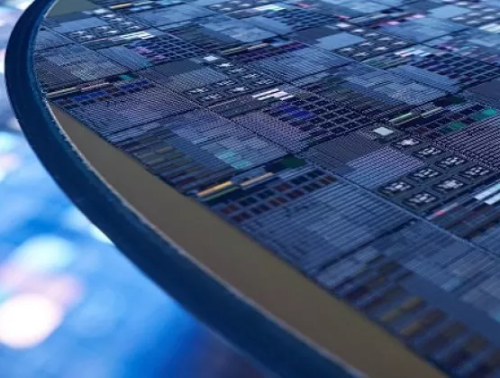
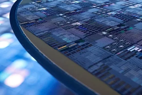
A lot has happened in fifty years, particularly when it comes to the microelectronics industry. Founded in 1970 by a group of semiconductor industry pioneers who believed that co-opetition — instead of traditional competition—would produce a more vibrant emerging industry, SEMI was born as an industry association.It's fitting during this week’s 50th annual SEMICON West (July 20-23, 2020) — a virtual event for the first time — that SEMI Chief of Staff Bettina Weiss offers her perspectives on the evolution of SEMI from one of the best seats in the house: the 24 years that she has spent helping the association change and grow.Vetrano: You’ve enjoyed a long rich history with SEMI, and now serve as the association’s first chief of staff. What roles have you played at SEMI up to this point?Weiss: I cut my teeth at SEMI by joining SEMI Standards, first serving as standards coordinator at SEMI Europe from ’96-’97. Over the next 11 years, I held a variety of positions at SEMI Standards, culminating with director of international standards from 2003-2008. Given that experience, I have to admit that SEMI Standards are still near and dear to my heart.I moved on to several leadership positions in our former global photovoltaics/solar business through 2014, and toward the end of that stint, I assumed additional responsibilities, becoming vice president of business development. That’s where I dove headfirst into expanding SEMI into emerging regions, including Vietnam, India and Latin America. SEMI goes where members see (or want to better understand) new opportunities, especially in places that had ambitious plans for fabs for microelectronics, including semiconductors and MEMS.In 2018, I became SEMI chief of staff, reporting directly to our president and CEO Ajit Manocha.Vetrano: Now I hardly know where to start! Since I have to decide, what does it mean to be SEMI chief of staff?Weiss: As the first chief of staff, I’ve been able to shape the position, combining the support of critical efforts driven by Ajit with additional project management responsibilities like our Smart Mobility initiative.Working with experienced leaders in our industry, such as the Board of Industry Leaders (BIL), is one of the more rewarding parts of my role at SEMI. The BIL is a group of global executives tasked with advising SEMI on strategic planning, especially when it comes to future-looking initiatives like Smart Mobility, Smart MedTech, Smart Manufacturing, and Smart Data/AI.A lot of the other things I do are meant to support the whole SEMI organization, in partnership with other senior leaders such as Michael Ciesinski, vice president of technology communities, as we create business plans and examine new revenue models that will keep SEMI sustainable and viable for the future. This includes issues as varied as workforce development and diversity and inclusion, and the new digital platforms we use to engage with our members.Vetrano: How does SEMI Smart Mobility initiative exemplify the model of engaging end customers in vertical markets that are important to members?Weiss: When you look at the rapidly increasing number of chips and sensors in and around vehicles, Smart Mobility at its core brings together both the semiconductor/sensor and automotive/mobility supply chains for a more transparent dialogue about needs and wants along the entire supply chain. We are thrilled to count automotive OEMs Volkswagen and Audi as SEMI members. We also work with Tier 1 suppliers such as Continental and many others to promote the open exchange of ideas and foster collaboration among all stakeholders.Smart Mobility is a good example of how SEMI connects two worlds that are now interdependent for the mutual benefit of all players. Automotive companies and component suppliers want to better understand new technology capabilities that enable tomorrow’s infotainment, safety, security and communication protocols. And semiconductor, sensor and component companies see huge upside in supplying the equipment, materials, devices and subsystems that enable the future of mobility. Smart Mobility is a win-win, and the founding concept of our Global Automotive Advisory Council (GAAC).Vetrano: As we look to COVID-19, the single most important event to influence the microelectronics industry — and every other industry — why is SEMI membership more important now than ever?Weiss: Our industry is facing a triple whammy of challenges: a global pandemic, ongoing global trade tensions that impact interdependent supply chains, and a global economic crisis. All these challenges will require our members’ ingenuity, innovation and collective action to overcome them. But inherent in those challenges are tremendous opportunities, and I have no doubt that our members and the entire global electronics ecosystems will find ways to help everyone prosper and advance.COVID-19 has had a huge impact on our members. From the onset of the pandemic, we’ve provided our members with resources including best business practices, insights and data from industry experts to help them respond to a virus that has already changed so many things we took for granted before March. Additionally, SEMI has also advocated with governments around the world on behalf of the industry for essential business status and essential travel to sustain operations. Visit SEMI COVID-19 Resource page for information on industry best practices and much more.Vetrano: Before we look forward, what has changed dramatically in microelectronics since you started at SEMI?Weiss: Through my work with SEMI, I’ve witnessed dynamic, dramatic and sustained change in the microelectronics supply chain. Into the late 1990s, SEMI represented primarily semiconductor equipment and materials suppliers, and we worked with chipmakers – our members’ customers. That’s where a lot of important Standards work happened, for example, and the supplier-device maker relationship was pretty much our world. Over the years, we saw significant change in how companies partner and do business with one another. The digital transformation we’ve been witnessing for the past few years was the impetus for expanding our reach to bring companies in the extended electronics manufacturing and design supply chain together, from sand to system, so to speak. That was also when we invited associations representing flexible hybrid and printed electronics (FlexTech), MEMS and sensors (MSIG), and electronic system design (ESD Alliance) companies to join SEMI and our other technology communities for maximum cross-pollination. That’s because everything needs microelectronic devices and systems. Vetrano: Looking ahead now, what is can the microelectronics industry do to benefit humanity?Weiss: Semiconductors and sensors are often the unsung heroes of progress. Microelectronics can help bring prosperity to the billions of people now struggling on our planet. It can improve access to education for people through e-learning, it can advance agricultural production and streamline the food supply chain to help feed the world’s hungry, it can monitor the quality of the water we drink and the air we breathe, and it can get you in front of a doctor even in the most remote village in India.The beauty of microelectronics is that we are not gated by innovation. As the brilliant visionary Arthur C. Clarke once said, “The only way of discovering the limits of the possible is to venture a little way past them into the impossible.”As an industry association that helps technologists to venture beyond “the limits of the possible,” I invite like-minded technology adventurers to engage with SEMI, starting with registration to this week’s SEMICON West – our first virtual show.As chief of staff, Bettina Weiss reports to SEMI President and CEO Ajit Manocha and manages a broad portfolio of responsibilities. Major focus areas include advancing specific global strategic initiatives such as thought leadership (Think Tanks) and SEMI Smart Transportation vertical application platform, improving organizational efficiency, alignment and financial sustainability, acting as senior liaison to SEMI Board of Industry Leaders, leading strategic partnerships and M A activity, and supporting Manocha in creating a highly effective, agile global association.Maria Vetrano is a PR consultant at SEMI.
Read More
Innovations in the public sector are springboards for new products in digital health and personalized medicine. Since 2013, SEMI NBMC, funded by the Air Force Research Laboratory (AFRL), has been evaluating industry needs and soliciting proposals for new research into the foundations of device development and manufacturing of medically actionable devices.SEMI NBMC has run 17 separate programs with more than two dozen organizational participants developing materials, electronics, microfluidics, manufacturing processes and algorithms to create low-cost, wearable sensors. Most of these integrated sensing systems communicate wirelessly and incorporate high-performance silicon devices that are designed to move with the individual. Each of the projects was the result of a proposal received during NBMC’s annual proposal cycle. ​What’s Next in MedTech Device Development?We invite you to join the teams at SEMI, NBMC and AFRL to answer that question in a virtual series of sessions over the four weeks in August.For the past five years, NBMC has been conducting similar sessions for roadmapping the development of non-invasive human performance monitoring technology and manufacturing. The information feeds into the topics for upcoming RFPs, including the one we expect to release in September 2020. Previous Workshops (formerly entitled Blood Sweat and Tears) brought together industry and university innovators to explore current product research and provided excellent insights for the proposal evaluation teams. We believe the insights are also very useful to the business and technology planning direction for researchers and developers working on these products.Our focus is on early-adopting markets – medical professionals and their patients, Army and Air Force personnel and high-performance athletes.​ In this time of social-distancing and overall hesitancy to approach hospitals and medical offices, medical monitoring that provides medically-actionable intelligence is of even greater significance.But Doesn’t FitBitTM Have that Covered?Advancements are coming fast and furious – but medical professionals and insurance companies are struggling to distinguish innovations that provide actionable intelligence from those that provide generalized, non-actionable data.The workshop will focus on the medically relevant information that requires a great deal more accuracy, testing and certification before decisions are made. It is the innovations in this field that will lay the groundwork for new products in digital health and personalized medicine. Additionally, they are leading to advancements in aeromedical monitoring and diagnostics to support the U.S. Air Force’s mission to improve patient care during emergency air transport. The targeted future state is real-time monitoring of biochemical and physiological markers that can guide optimization of human performance and health. ​The SMART MedTech Virtual Workshop Series will link markets with manufacturing for medical relevancy – addressing both ends of the ecosystem. This forum will bring together the players across the growing range of industries that are entering or advancing human monitoring applications to:​ share competitive ideas that may be applied to product development​, assess roadblocks in bringing human monitoring products to market, and form partnerships that have become key in overcoming obstacles to successful manufacturing and product development. ​ Join the experts who are at the cutting edge of product design and manufacturing techniques. Indeed, the success of previous workshops was based on the unique membership of NBMC, where product and manufacturing-oriented engineers from industry, universities, and government labs form teams and pool resources (financial as well as technical) to accelerate human monitoring product development into manufacturing prototypes.Can’t Attend the Workshop?All sessions will be recorded and available for watching and re-watching on-demand. Join our interest list to receive regular updates on SEMI NBMC activities, including notification of the RFP expected to be available in October 2020.Find out more about the Smart MedTech Initiative and the NBMC Programs at our website.Rene Krantz is Director of R D Programs Business Development at SEMI. She is the primary manager of SEMI Smart MedTech Initiative and NBMC programs. Contact Rene at [email protected].
Read More
The COVID-19 pandemic has inflicted major impacts on manufacturing operations worldwide including in the semiconductor industry. The virus has left millions of people confined to their homes, resulting in a massive shift to virtual work and online engagement. In Singapore, where AEM is headquartered, our management team took proactive measures to protect our workers by implementing best practices ahead of the Singapore Circuit Breakers.AEM is globally deemed an essential service, requiring us to maintain operations and minimize impact to our customers. Business continuity plans that include work-from-home and safe-distancing guidelines are in place. As of the time of this writing, we are very fortunate that all of our employees are safe and that we’ve seen only minimal impacts to our customer commitments. AEM has confined this impact by spreading operational risks across our facilities in Asia, Europe, the U.S. and divisions in Singapore, Malaysia, China, North America, Central America, Finland, France and Vietnam. All told, these facilities employ more than 550 people (Figure 1).Figure 1 – AEM Global Presence As a global leader, AEM offers application-specific intelligent system-level test and handling solutions for semiconductor and electronics companies that serve the advanced computing, 5G communications and artificial intelligence (AI) markets.Leveraging our decade of experience, the latest AMPS solutions provide asynchronous, modular, massively parallel and smart system-level testing to meet the new test challenges of complex ICs. The modularity and scalability of these systems enables customers to scale their existing engineering device validation solutions into high-volume, massively parallel production solutions that increase faults coverage, reduces time to market, and decreases cost of test and ownership (Figure 2).Figure 2 – AMPS System-Level Test Solution In meeting 5G infrastructure test needs, AEM developed a field-deployable fiber optics tester. Called WideOptix SR4, the system was initially developed in collaboration with a world leader to support the 5G fiber infrastructure deployment in China and has now been adopted for some Ethernet standards testing. With our WideOptix SR4 development, we cultivated Silicon Photonics (SiPh) testing expertise that complements our AMPS system-level test capability. As part of our business continuation and risk diversifications plan, we had also set up factories in Penang (5,200m2) and Suzhou (3,600m2). Penang’s rising influence in the Southeast Asia semiconductor industry has prompted AMM (AEM Malaysia) to expand its scope to include value-added services with a Center of SSD Excellence and Center of Photonic Excellence.ASZ (AEM Suzhou) will continue to focus on the domestic market in China for further expansion and penetration with products ranging from cost-sensitive testers to state-of-the-art test measurement instruments. In Europe, AEM is focused on wafer-level test and cost-effective ATE test solutions. Finland-based AFORE specializes in MEMS and application-specific wafer testing with the ability to add physical stimulus. The company's state-of-the-art instruments enable the testing of devices such as diced IMU’s (Inertia and Motion Units) in continuous rotation on a wafer mounting ring. Our process increased test throughput by 3X compared to the traditional pick-and-place methods (Figure 3).Figure 3 – Wafer-Level Test Throughput Advantage A specialist in application-specific wafer handling, AFORE developed its latest design to support quantum computing in collaboration with its partner BLUE FORS. The company’s probing equipment features a handling solution with temperature tolerances to 2K (-270’C) to support cryogenic testing (Figure 4).Figure 4 – Cryogenic Quantum Computing Probing Solution AFORE also gained critical insights into creating total darkness, enabling us to further explore opportunities for dark matter testing. AFORE is currently in talks with a member of the LUX Photonics Consortium funded by the National Research Foundation (Singapore) to provide a dark body testing environment and handling for its IR detectors.In Europe, our acquisition of Mu-TEST in France helps diversify our product and service offerings while spreading our business continuity risks. Mu-TEST enjoys collective test-development experience of more than 320 man-years thanks to various ATE suppliers including Schlumberger and Credence. To help combat rising costs of traditional ATE, Mu-TEST developed cost-effective solutions using FPGA-based instruments supported by a full suite of test development, debug and production test software with links to EDA and standard interfaces. This provides Mu-TEST an agile platform that can be easily re-configured for different customer needs.This Mu-Test acquisition expands AEM’s system-level testing capability to include Functional Test, allowing BIST, SCAN, JTAG to test structural failures and perform other application-level test that interface directly with the DUT using the EVM (Electronics Validation) boards to increase fault coverage within the same test environment. Mu-TEST has also enabled AEM to form the recent partnership with UTAC to develop a cost-effective CIS test solution that addresses UTAC’s test needs and complements its CIS advanced packaging solutions. Our U.S. headquarters based in Chandler, Arizona has expanded its capabilities to provide application engineering.In summary, AEM has been expanding its global footprint while managing risk and has been fortunate to be positioned to manage the recent COVID-19 excursions. While each geographical location specializes in core technologies, all sites have access to one another’s manufacturing facilities in times of need and a pool of IP available to address new opportunities. We believe this risk diversification positions us well to serve the needs and interests of our customers worldwide.Lo Wee Tick is Director, Business Development, and Stuart Pearce is Senior Director, Field Marketing, at AEM Holdings Ltd.
Read More
As the COVID-19 quarantine-related restrictions for commerce and transportation are lifted in the Philippines, companies are dusting off desks, cleaning coffee mugs, warming up equipment and gradually bringing back staff to resume full operations. Of primary interest to manufacturing companies like Microchip Technology Philippines are the restrictions on the allowable workforce, the movement of personnel, transportation, and health and safety protocols affecting factory staffing, materials availability, and the ability to ship products. In the Philippines, these restrictions started to scale back in mid-May and are staged to continue in a series of continuing reductions every two weeks through the end of June. As business operations recover, challenges remain in managing the workforce, negotiating the supply chain and understanding the expenses required to operate under the “new norm” while Business Continuity Plans continue to be reviewed and revised.Here are some of the more important business-related elements of the quarantine levels enacted by the Philippines:Enhanced Community Quarantine (ECQ): In effect from March 17 through May 15, 2020, this was the initial lockdown with the strictest requirements, most notably requiring the general population to stay at home, imposing curfews, prohibiting all public gatherings including schools, halting public transportation and banning air travel while allowing cargo flights, skeletal workforces (~15%) for essential businesses (BPOs, IT and exporters, for example) and travel using some private vehicles with varying types of passes required to clear checkpoints.Modified Enhanced Community Quarantine (MECQ): In effect from May 16 through May 31, 2020, this was the first stage to ease control to allow up to 50% of employees to return to work at essential businesses. The easing also allowed gatherings of up to five people while maintaining most other restrictions.General Community Quarantine (GCQ): In effect from June 1 through June 15, 2020, essential businesses are allowed to resume full operations within health and safety protocols in place for physical distancing, disinfection and the wearing of Personal Protection equipment (PPE). Air travel is allowed to resume while public transportation remains restricted until June 21, 2020. Company shuttles are allowed for point-to-point services.Modified General Community Quarantine (MGCQ): Planned for June 16 through June 30, 2020, this is the transition phase to the “new normal,” which will continue easing the restrictions for contact-related businesses such as barbershops, salons, restaurants and the like. Movement and public transportation will remain restricted until June 22, at which point the last obstacle for businesses to fully resume operations will fall.While some larger companies during the most restrictive ECQ were able to house staff on site or nearby in skeletal crews, some smaller companies were unable to do so and may never recover from the loss in revenue or from the loss of employees. The majority of companies in the technoparks shut down under the ECQ and were rendered powerless to return workers to factories. For factories allowed to house employees on site, a huge effort was required to provide emergency transportation, accommodations, food and drinking water, toiletries, Wi-Fi, and even entertainment for the sequestered staff – all while maintaining health and safety protocols for physical distancing and disinfection. For example, Microchip Technology Philippines was able to build temporary sleeping cubicles and showers; to buy tents, foam mattresses, bedding and personal hygiene kits; to provide canteen and laundry services; and to allow Wi-Fi access for employees to stay connected to family and friends.Microchip Technology’s 11 Guiding Values help to define our corporate culture and guide our decision-making. One key Guiding Value on display as we’ve transitioned through the levels of quarantine due to the COVID-19 pandemic has been that Employees Are Our Greatest Strength. Exercising this Guiding Value has supported the expenses necessary to provide the safest, most comfortable living accommodations in the factory conference rooms, hallways, basement, and even in office cubicles.While many larger companies in the Philippines provide company shuttles at pre-established pick-up points, limited public transportation strands many workers at home with no way to reach to their assigned shuttle. To address this challenge, solutions including van brigades that can navigate narrow village streets to pick up workers should be considered though at an additional, unplanned expense. The physical distancing rules effectively halves the number of riders, which in turn requires a doubling of the shuttle buses, most of which are under lease. If shuttle bus leasing companies cannot provide more buses, employees who can work from home should continue to do so or drive to shuttle stops if they have personal vehicles. Leasing these additional shuttle buses was in no company’s budget as we began 2020.Additional measures under the new norm will be expensive – perhaps prohibitively so – for smaller companies that cannot afford to double the number of company transports due to physical spacing rules requiring them to halve workplace capacity, whose workplace environments cannot support physical distancing, and whose treasuries cannot afford to buy rapid test kits for employees and their families. If these smaller companies produce items critical to the supply chain, larger companies will feel the sting – and cease producing specific products during the qualification of an alternate supplier. Until the Bureau of Customs and staffing of third-party logistic providers is back to normal, and until ports are running at full force, materials and exports will continue to be delayed, potentially limiting the number of employees needed to return to work to run production.It has been very expensive for companies to survive through these levels of quarantine while keeping factories and employees in a state of readiness to return to work. Additional expenses will be borne for compliance to the new norm. As many businesses recover under the new norm, they’ll undoubtedly take a closer look at their business continuity planning, if any such plans exist, and if not, they should be created without hesitation.The problem with a typical business continuity plan is it tends to focus on one or a few concurrent major events – say, flooding or a power failure due to a typhoon – but it’s doubtful any plan took into account a global pandemic that affected so many factors simultaneously including workforces, supply chains, transportation, logistics and food supplies. As we return to work, we’ll have to adjust to the new workplace and embed the lessons learned during the COVID-19 pandemic into our business continuity plans. And, hopefully, we’ll never have to exercise those measures again.Greg Fisher is Managing Director at Microchip Technology Philippines.
Read More
By Sowmyan Rajagopalan, Founder and CTO, Thalia Design Automation FD-SOI is receiving significant traction with analog designers, but analog IP reuse often equates to tough choices. Porting chips from bulk to FD-SOI or creating new chips on FD-SOI means making decisions on porting existing bulk IP or starting from scratch. To invest the time and resources in reusing an analog IP requires a judgement call on the potential returns from the market and the time it takes to get the IP to that market to generate revenue is key – if a competitor's project hits the market first, then the potential returns are greatly diminished. There is also a need to understand the differences in process technologies and the impact those differences have on the efficient reuse of analog IPs. All this means that the demands on resources and time are high. Decisions, decisions A typical decision fork faced by many companies is whether to design new IPs, or if they should instead build a portfolio of analog IPs. Given the opportunity cost, availability of resources, time and resources needed for each option means that doing both is a difficult option. Both have their advantages; designing new IPs allows companies to branch out and address new sectors or markets. New IPs often demand higher revenues and engages in-house designers as the work, by its nature, is more innovative and challenging. On the other hand, building a portfolio of analog IPs allows companies to expand in an existing market, bringing stabilisation and strengthening revenues from existing product sectors. But why should you have to choose when there’s a third option? Have your cake and eat it It is difficult for a company to drive both options internally – not least because there’s a paucity of good analog designers in the market, and the opportunity cost is simply too high. However, the good news is that firms like Thalia have the specialist expertise and toolsets required build a portfolio of analog IP, saving time and investment while in-house designers focus on new IP design. Looking back Over the last 18 months, there has been a rapid uptake of FD-SOI process technologies. With production at foundries such as GlobalFoundries and Samsung now in full swing, more and more analog designers are reaping the benefits of FD-SOI. At Thalia we’ve been at the forefront of some of these changes, having worked with multiple customers on projects that use FD-SOI technology. [bctt tweet="More more analog designers are reaping the benefits of #FDSOI. At Thalia we’ve been at the forefront of some of these changes, having worked with multiple customers on projects that use FD-SOI technology. - @Thalia_IP_Reuse CTO " username="soiconsortium"] Driving the shift to FD-SOI [caption id="attachment_34410" align="alignright" width="347"] (Courtesy: STMicroelectronics)[/caption] This figure contrasts the structures of traditional bulk planar and SOI type transistors. The main difference is the inclusion of a buried oxide layer that isolates the channel of the transistor from the bulk silicon of the substrate. This results in a very thin, controllable channel structure, with much lower leakage currents being ‘lost’ into the device substrate than traditional alternatives. This in turn improves two key figures of merit for the device. First, standby power consumption is dramatically reduced. Second, the threshold voltage is much more predictable and controllable – yields are improved, and power/performance tradeoffs via voltage scaling are more easily enabled. The penalty is that FD-SOI transistors are generally not so fast. But one other feature of the technology – particularly important for mixed signal and analog designs – allows smart designers to mitigate this effect. Biasing the body structure at a different voltage to the source enables the designer to trade speed for power: a reverse bias increases the threshold voltage of the device, making it slower, but reducing leakage current; conversely, forward biasing reduces the threshold voltage, increasing the speed of the device, at the cost of power. Design migration Thalia has worked on a number of projects that utilize SOI technologies. A recent RF front end for Bluetooth Low Energy (BLE), for example, used exactly the techniques I have outlined above. We migrated an entire subsystem design, composed of around 30 blocks (including ADCs, PLLs, mixers, amplifiers and power controllers), to a 28nm Samsung FD-SOI process. [caption id="attachment_34412" align="alignright" width="451"] Click on this slide to see a YouTube video of the full Thalia presentation given at the Design Reuse FDSOI Virtual Event in March 2020.[/caption] The circuit was verified for compliance with design specifications. Design changes were implemented to ‘nudge’ the design to meet the requirements. And we made full use of the body biasing techniques I have already outlined. We used reverse body biasing to keep leakage as low as possible in parts of the circuit in which speed was not a factor; and, where speed was a key requirement, implemented forward gate biasing to increase performance. We’re expecting increasing numbers of customers to start moving their analog and mixed signal designs to SOI technologies in the coming months and years. The process is not without its challenges: but with an intimate knowledge of circuit design and optimization, and of the subtleties of the processes themselves, there are substantial advantages to be reaped. Technology analyzer – identifying the root cause when circuits fail A large part of the effort involved with migrating an IP from one technology to another is involved with qualifying the IP in the target technology; if a block doesn’t meet the requirements of the target technology, it won’t function. Identifying the cause of this – the technology characteristics that cause it – and then addressing them is key to a successful outcome. Whenever a key specification is not being met in the target technology, we have to determine which process technology or circuit characteristic is causing this. By using our automated technology analyser, we can take a design-centric approach to analyse and compare base and target technologies to see where the process technologies are similar and where they differ the most. The technology analyser considers both first and second order effects including FT, gm/id, Vdsats among others. Using this technology, we can identify which characteristics differ between the origin and target technologies. With traditional methods, identifying differences in characteristics would be time consuming, but our technology analyzer gives a clear and rapid identification of the issues, allowing us to fix any mis-matched topologies and achieve a functioning result in the target technology. The reality? IP reuse is not a dream or a myth Our platform comprises three elements – Technology, Methodology and Design Expertise. Using this trifecta, we have been able to deliver IPs in different technologies, nodes and with improved characteristics. The AMALIA technology consists of four elements: a technology analyzer, schematic porting, design enabler and layout migration. Tech analyzer: Using a design-centric approach, the platform addresses key first and second order effects of process technologies and extracts and compares characteristics between base and target technologies to provide the user with clear inputs on how similar the technologies are. Automated schematic porting: Taking the inputs from the analyzer and generates a circuit in the target technology. This circuit can then be verified for response and characteristics. Design enabler: Once the circuit design for the target technology is correct, the design enabler and our team of experienced designers can nudge the circuit back into specification. Layout migration: The final stage is focussed on putting together the base layout framework which is then expanding on by our experienced layout designers. Who we are?We are Thalia Design Automation. I founded Thalia in 2011, with the aim of improving the efficiency and process cost of analog circuit design and to rollout an analog IP reuse platform. We’ve worked with vendors, numerous foundries and different nodes and have design centres in Germany and India with our headquarters in the UK. We have successfully rolled out an analog IP reuse platform that combines smart technology, a smart methodology and our smart and experienced resources to streamline the IP reuse process. In doing all this, Thalia regularly provides customers with a time saving of around 50% compared to a traditional circuit redesign. And as I stated at the beginning of this article, achieving a faster time to market is key to maximizing revenues from any IP.
Read More