downloadGroupGroupnoun_press release_995423_000000 copyGroupnoun_Feed_96767_000000Group 19noun_pictures_1817522_000000Member company iconResource item iconStore item iconGroup 19Group 19noun_Photo_2085192_000000 Copynoun_presentation_2096081_000000Group 19Group Copy 7noun_webinar_692730_000000Path
Skip to main content
Default Banner Image

Technology and Trends

Not long after STMicroelectronics opened its first semiconductor plant in Singapore more than 50 years ago, a facility chiefly focused on chip assembly and packaging, the company realized that it had constructed the site in an area with a blossoming chip ecosystem with a bright future. Before long, the company became the first to start a wafer fab facility in the so-called Little Red Dot. Today, our STMicroelectronics Singapore campus sports several buildings that dwarf the original site in the sprawling Ang Mo Kio Industrial Park 2. The facilities feature advanced 200mm manufacturing lines but still produce huge volumes of chips with more than 1,000 pieces of 150mm manufacturing equipment.Much of the wafer equipment dates back to the past century so is no longer supported by the manufacturers, if they’re still even in existence. Yet decades later the chipmaking gear continues to operate with a surprising reliability that far surpasses the longevity called for in its manufacturing specifications thanks to replacement parts and frequent upgrades with more sophisticated handling robots and chucks. Now, as smart manufacturing begins to establish a foothold in the semiconductor industry, Industry 4.0 technology is breathing new life into these aging workhorses.Despite its age, all of the equipment adheres to industry manufacturing standards. The gear is remotely controlled using the SECS/GEM interface protocol that was either originally integrated with the equipment controller or custom-made. We’ve also maximized its usage through advanced recipe management, advanced alarm and event handling, and secured lot identification.Crucially, we decided to systematically deploy a real-time fault detection and classification (FDC) solution using a third-party product based on what today is known as an edge computing architecture. Every piece of critical processing equipment is progressively paired with its dedicated FDC instance running on a virtual machine in the wafer fab data center, and the FDC solution monitors vital equipment parameters at high frequency – depending on the SECS/GEM capabilities of the equipment – and analyzes incoming manufacturing data in real time using classic SPC (statistical process control) algorithms and even AI-class protocols.Our use of the FDC edge solution as a sensor signal aggregator has given our equipment a second life. The solution processes real-time signals from sensors connected through a typical TCP-IP. Sensors have been the old equipment’s saving grace with their ability to de-multiply equipment capabilities and overcome fundamental shortcomings and design weaknesses. The STMicroelectronics Singapore plant first used off-the-shelf sensor nodes with built-in power amplifier and analog input nodes. While very practical and easy to implement, deploying the nodes can be costly. After developing more expertise in sensor integration using FDC, our wafer fab equipment experts decided to design an in-house solution based on the famed STM32 microcontroller. Leveraging Arduino – an open-source electronics platform with easy-to-use hardware and software – the equipment teams can now design and program a variety of in-house sensors for measurements including temperature, humidity, waterflow and pressure. The sensors are integrated with process equipment using the FDC solution. Integrating the sensors with the FDC engine on the edge computer extends the capabilities of old equipment without jeopardizing the integrity of the machines themselves. While the integration can be quick, it must be robust to ensure the reliability of the new measurements. Similarly, ever-increasing connectivity requirements present clear cybersecurity risks that must be managed upfront and each solution must be hardened to minimize security vulnerabilities. Even so, the challenges and risks pale in comparison to the benefits! Jean-Marc PHILIPPE is DIT Director at STMicroelectronics Pte Ltd. He oversees the deployment and support of Digital Solutions to enable STMicroelectronics front-end operations in Singapore and manages manufacturing productivity and automation programs at site level.
Read More
Semiconductor process development is no easy task, with each generation of devices more difficult and expensive to create. Traditional cycles of build-and-test development are becoming obsolete, since they are too expensive and time-consuming for the most advanced processes.The High Cost of Process DevelopmentMost chip designers developing new products rely on existing manufacturing processes, but someone had to create those processes to make the designs possible. The goal of process development is to create new semiconductor manufacturing processes that provide high yield while achieving the required device performance. In contrast to new chip design, however, it requires an entirely different set of engineers and skills.The traditional approach to process development involves building multiple test wafers to determine the ideal process for a given device. After one set of wafers is fabricated and analyzed, insights from the previous round help to refine process steps for another round of fabrication. Due to smaller feature sizes, each new process generation is more sensitive to variation. This adds even more complexity because smaller feature sizes and parasitic effects require more measurements and testing as well as additional fabrication. The cycle is repeated many times before the entire process flow can be finalized, making it time- and cost-intensive, especially for the most advanced technology nodes.Testing Virtual Wafers Instead of Real WafersToday, there is an alternative to this slow, expensive way of doing things. Virtual fabrication lets computers simulate all of the processing that occurs when real wafers are built. These virtual models allow semiconductor process engineers to test manufacturing equipment settings with far greater variation than is possible in a physical fab. Designers can simulate the entire process flow, running the equivalent of thousands of wafers in days instead of months. Designers can quickly see graphical animations to visualize process steps, modify process recipes and device geometries, and measure how these changes affect electrical behavior.Improving Yield Using Statistics in Virtual Wafer FabricationBecause of the high volume of data generated, designers are turning to statistical analysis to provide greater confidence in their choice of process settings. Defects and random variations can be modeled in a virtual fab in a way that’s not possible in a real fab, letting developers test the sensitivity of the device structures against the unpredictable aspects of processing.There’s more than one approach to optimizing the process settings used in a new memory or logic fabrication sequence. The simplest one involves taking a single variable and exploring its effects. Critical dimensions (CDs), for example, establish those feature sizes of a device that ensure desired electrical performance. A particular dimension can be swept from low to high values – developers can then measure the effects of that range on device behaviors such as threshold voltage. This allows developers to ensure that the electrical behavior of their device design addresses the range of expected feature sizes and variability. The interactions with intersecting process steps can also be tested for further validation, since these interactions can lead to unanticipated device performance.But, in reality, this approach isn’t sufficient for studying the complex web of interactions between process steps and the resulting structures.A second approach leverages Monte Carlo analysis, randomly varying a wide range of process and device parameters and calculating the resulting device geometry and performance. This data can be used to automatically identify the process and design settings needed to achieve yield and performance goals. It’s an area where simulation shines, providing a useful way to test the interactions between many different processes.Statistical experiments using virtual fabrication illustrate step-by-step methodology to optimize process and design settingsVirtual Fabrication PlatformSEMulator3D is a virtual fabrication platform created by Coventor, a Lam Research company. It allows the definition of all process steps, the modeling of devices, the collection of metrics, electrical and device analysis, the statistical analysis of results, and the visualization of process steps through graphical animation. Today, semiconductor companies use it for both optimizing and scaling leading process nodes and for developing advanced new technologies like GAA (Gate-All-Around) transistors.The ability to do this work virtually is the future of semiconductor process development. Virtual fabrication accelerates new process time-to-market by months, opening up market opportunities worth hundreds of millions of dollars for semiconductor companies.Visualization of process steps of a Gate-All-Around transistor shows 3D construction in SEMulator3D. To learn more about virtual fabrication and how it’s changing the future of semiconductor technology development, download our whitepaper Speeding Up Process Optimization with Virtual Fabrication.Lam Research is a longtime member of MEMS Sensors Industry Group®, (MSIG), a SEMI technology community that connects the MEMS and sensors supply network in established and emerging markets, enabling members to grow and prosper. Visit us today.David M. Fried, Ph.D., is vice president of Computational Products at Lam Research, where he is responsible for the company’s strategic direction and implementation of virtual process solutions, including the Coventor SEMulator3D virtual fabrication 3D process modeling solution. Fried leads the execution of technology strategy for technology platforms, partnerships, and external relationships. His expertise touches upon such areas as Silicon-on-Insulator (SOI), FinFETs, memory scaling, strained silicon, and process variability.Fried is a well-respected technologist in the semiconductor industry, with 60 patents to his credit and a notable 14-year career with IBM, where he was involved in successive process generations from 65-nanometer and lower. His most recent position was 22nm chief technologist for IBM’s Systems and Technology Group. He holds bachelor’s, master’s and doctoral degrees in Electrical Engineering from Cornell University.Republished with permission from Lam Research.
Read More
Incize has been active in characterization for RF-SOI since its creation in 2014, what are your insights on the RF-SOI industry and 5G technology today?Today, the number of foundries developing switches on RF-SOI is increasing, and this trend will continue for the next few years. We saw this opportunity a while back and invested in it. There is no current viable competition for RF-SOI – nothing will replace it in the short term. There are other technologies, but to replace RF-SOI, this is something only imaginable on the long term. It is a stable market with high demand. Other components of the Front-End-Module (FEM) are also moving to engineered substrates (SOI), and Incize enables its customers to develop these technologies. For the foundries wishing to introduce new engineered substrate (SOI), we help understand the physics behind the technology so that they can migrate to SOI. We help develop test structures and evaluate the technology. From conception to product launch, Incize is the partner of technology enablement. Concerning the 5G market, we see other engineered substrates that will surely appear on the market in the long term, this is why we also highly invest in R D to uncover the next generation engineered substrates and be ready to help our clients with this integration. What is Incize’s added value for customers? Starting as a spin-off from ‘Université Catholique de Louvain’, and established in 2014, Incize’s debut focused on characterization of SOI technology. Today, Incize has enlarged its service portfolio and can be characterized as a technology enabler and partner for engineered substrates and RF technologies. We believe RF is an art and we help you to see the whole picture. Incize customers are wafer suppliers, foundries and fabless companies. The services we offer are testing and modeling of materials and devices used for Radio Frequency (RF) applications. Depending on the use of the substrates, we realize tailored testing and modeling to improve the technology and tune processes. Although big players have teams devoted to this, thanks to our expertise built up over the years our added value is to undertake advanced tests and modeling that customers can not do; with RF SOI being one of our specialties. Incize has seen a steady year-on-year growth and today is built up of a team of 10 full time employees dedicated to finding the solutions to our customer’s problems. 3. Could you please tell us more about Incize's R D capability and state-of-the-art technologies in getting ready for 5G? Incize is also very active in research and development in order to continuously stay ahead of the game and provide innovative and state-of-the-art solutions to our clients. 5G is at the verge of tomorrow, although still not well defined (especially for the mmWave band), requirements are getting more challenging. Once the technology is well understood it can be implemented. Foundries and fabless need our help to do it fast and do it well. It is by working together that we will create great value. Currently we have 7 ongoing research projects. Our research projects address new materials as well as new challenges in design and characterization for 5G communications systems/technologies and beyond. New materials required to fulfill the stringent requirements imposed by the 5G standards are being investigated. Phase changing materials, piezoelectric materials, porous silicon and III-V materials will be incorporated in the new generations of front-end-modules which will be part of the mainstream RF electronic industry on the long run. Our projects are tailored to investigate the performance of these materials as part of the next generation of substrates and to develop appropriate characterization techniques to benchmark state-of-the-art 5G devices. Porous Silicon has been largely studied at Incize and we now offer our customers a complete solution from idea to prototype. For our clients we realize feasibility studies, R D, characterization, modeling and prototyping. We carry out various customizable process in a R D technological platform dedicated to microfabrication. Whether you wish to integrate porous silicon before or after the fabrication of devices, Incize is your dedicated partner. We have also been actively researching piezoelectric materials such as quartz, LiNbO3, LiTaO3, ZnO and more in order to fully understand their properties. We have been actively studying new characterization techniques for this fast-growing market. Whether you want to characterize or simulate piezoelectric materials Incize can help you in this trajectory. One of our research projects is specifically centered on RF-MEMS (Radio Frequency-Micro ElectroMechanical Systems), it aims to increase the skills of Incize in the fields of experimental characterization of these devices. Given the heterogeneous nature of MEMS, the test system must be as complete as possible in order to be able to monitor and collect amaximum of data on the various parameters of the component. RF-MEMS technology can be portrayed as an enabling solution to realise the high-performance and highly-reconfigurable passive components that future 5G communication standards will demand for. Incize will develop not only a RF-MEMS component test service, but also commercial test solutions for manufacturers of MEMS-RF components in order to speed up qualification on production lines. Incize is ready to embark on the road ahead to 5G technologies and beyond.
Read More
Call it a wild guess, but I suspect I am not the only follower of the automotive industry who is tired of reading articles that lament the impact of Covid-19 and speculate, to varying degrees of accuracy, what kind of recovery is in store for major automotive markets around the world.I’m much more interested in what solutions and creative approaches people, companies, and countries have come up with to make cars smarter and safer despite the pandemic or even because of it.A friend of mine who works at a major European vehicle OEM told me that “innovation cannot, must not stop – despite current difficulties.” This sentiment echoes through the automotive supply chain, particularly in the resilience of the semiconductor industry during these challenging times.The recent publication of the AspenCore Guide to Sensors in Automotive – Making Cars See and Think Ahead is a refreshingly positive and inspiring collection of articles, interviews, technology deep dives and business news, all carefully curated and edited by AspenCore Global Editor-in-Chief Junko Yoshida.One article I particularly enjoyed was her “6 Trends on ‘Perception’ for ADAS/AV.” The insights she was able to gather from experts attending the AutoSens show in Brussels are fascinating, even if consensus on what, exactly, will be the winning “robust perception” solution appears to be far off. This is only fitting with so many companies elbowing for that prime spot!Another feature article that stood out was Nitin Dahad’s “Level 5 AVs Unlikely Before 2035” article. It wasn’t so much the longer ramp to full autonomy that caught my eye but the daunting challenge the automotive industry and AVs have to tackle: “…all possible unusual driving situations under all driving conditions and in all environments.” This is truly a mind-boggling undertaking. The author argues that the road to Level 5 “is likely to be paved gradually, as more advanced driver-assistance features come to market.” Sounds reasonable.Both these articles point to the need for collaboration across the automotive electronics supply chain in order to not only sustain the pace of innovation, but accelerate it, as we face our current challenges. This made me think about the SEMI Smart Mobility initiative and how the great minds supporting it might be able to help. The initiative is designed to bring together automotive OEMs, Tier 1s, device makers, design houses, equipment and materials companies as well as R D institutes to address shared challenges and opportunities.SEMI used to stand for Semiconductor Equipment and Materials International, but over the past several years – and driven by the advent of IoT, AI, and everything “smart” – we now represent the entire electronics manufacturing and design ecosystem, with more than 2,400 member companies on our global roster. We created the Smart Mobility initiative in late 2017 with the initial goal of connecting a substantial number of members to new business opportunities involving rapidly rising silicon content in automotive. IHS Markit projects automotive semiconductor revenue to continue to grow at a 6% CAGR to 2026.Over the past 2 ½ years, the initiative has quickly evolved into a global platform connecting the semiconductor, sensor and automotive electronics ecosystem under one roof – the Global Automotive Advisory Council or GAAC. While “silicon content” is still the operative word for many of our core members, the Council’s mission is to address opportunities and challenges that impact more than one segment of the value chain. For example, the challenge of getting to zero defects involves just about every stakeholder – from contamination control in wafer carriers to ensuring device reliability and robustness to packaging and, ultimately, system integration in the car.SEMI also encompasses a number of Technology Communities that provide deep technical expertise in support of the GAAC’s mission. Member companies in our MEMS Sensors Industry Group (MSIG) are directly engaged in and contributing to the GAAC work. GAAC Europe Chapter - Participating Companies“Sensorizing” – making things smarter through the application of sensors – has created solutions for the automotive and mobility space that bring innovation, safety, security and comfort to driver and passenger and that benefit the environment around the car.This makes the AspenCore Guide to Sensors in Automotive a great resource for our members and SEMI staff as we collaborate to accelerate the drive toward Level 5 autonomy.If you are interested in learning more about SEMI’s Smart Mobility and the GAAC, please contact Bettina Weiss, Chief of Staff and Global Smart Mobility Lead at [email protected] with permission from EE Times.
Read More
I recently spoke with Chan Pin CHONG, Executive Vice President and General Manager of Products and Solutions at Kulicke Soffa, about how smart manufacturing is driving new production efficiencies in the semiconductor industry. During our conversation, he also provided practical steps for factory operators to follow in evaluating their smart manufacturing needs in order to ensure successful implementation and discussed the potential payoffs. Based in Singapore, Kulicke Soffa is a leading global provider of ball bonding, advanced packaging, wedge bonding, and electronic assembly equipment for the semiconductor, power and automotive industries.Ng: Industry 4.0 and smart manufacturing are critical to the growth of the semiconductor industry. What does the smart manufacturing movement mean to you or Kulicke Soffa?Chong: The future of smart manufacturing is the vision of building a digital connected factory to drive new manufacturing efficiencies by combining physical and cyber technologies. Industry 4.0 integrates discrete systems and harnesses the power of large volumes of data to move towards greater automation.At K S, we define smart manufacturing across the following four key areas embedded in our roadmap for all K S products, from wire bonders and advance placement tools to pick and place machines: Interoperability – This is about machines, devices and sensors connecting to each other. In fact, the very basis of smart manufacturing is that all devices are connected. Information transparency – Through simulation, various artificial intelligence (AI) tools use contextual information to emulate the actual world. Technical assistance – Robots or machines support humans in making decisions or solving problems. Autonomous decision-making – This is our vision that robots or machines can learn from machines to make decisions on their own. Ng: Please elaborate on some of these areas and how they’re the relevant to smart manufacturing. Chong: The need for machines, devices and people to communicate with each other forms the basis of connectivity, the idea of all machines communicating with each other or a host. Connectivity protocols now in place for machine-to-machine connectivity include SEMA, SECS/GEM, SEMI-ELS and IPC-CFX. Machine technology uses various sensing technologies. For example, for a pick and place machine such as SMT platform on K S Hybrid, the algorithm to recognize and align processes is part of the sensor needed in each machine before to can process and add thousands of components to the substrate or panel. In a wire bonder, the ultrasonics or EFO signal can provide some form of sensing technology for a machine to detect process conditions. Importantly, these sensing technologies can be used to collect feedback for process improvements.One example of how K S machines are connected to the host is our use of an intermediate server or host named KNeXt to connects to all assembly equipment in the fab. The equipment can then, in turn, connect to an external secured cloud or K S Global Cloud.Ng: What are the objectives for smart manufacturing?Chong: The ultimate goal is to achieve higher factory productivity or better OEE (Overall Equipment Effectiveness) by improving machine yields, productivity and efficiency. The key is to leverage AI, 5G, the Internet of Things (Iot) and other industry 4.0 technologies to drive automation and process improvements. Ultimately, each factory must meet productivity, yield and cost goals. Smart manufacturing enables factory operators to meet these goals. That is the focus of smart manufacturing.Ng: What is the biggest potential benefit of smart manufacturing?Chong: Smart manufacturing uses data to predict outcomes of a process step or machine operation. Once data is available in the global cloud, analytics can start to build data sets to run statistical modelling and examine factory operation trends. We can also use the data to identify past machine behaviors in order anticipate outcomes, including undesirable ones that we can then prevent.In the SMT example, if we can systematically examine days or weeks of historical performance, we can plot some statistical variations in the process specifically to a pick or placer or a robot and anticipate or avoid problems. However, all sensors must be in place in the bond head or the robot so that we can detect changes or variations in the robot’s movements.Kulicke Soffa smart manufacturing facility Ng: What are some recent factory improvements smart manufacturing has enabled? Chong: Kulicke Soffa has contributed to the hierarchical architecture of the smart factory and key technologies. COVID-19 is driving demand for greater factory connectivity, and K S offers solutions that are key to remote management and full control of smart equipment from a central control and embedding Internet of Things (IoT), big data, cloud computing and sensors in manufacturing. Using these technologies, a small smart factory can be remotely operated and managed.With COVID-19 limiting air travel around the world and access to support engineers, the need has grown for remote machine access to reduce the downtime per machine. Remote factory access enables off-site engineers to remotely identify and diagnose machine problems.Ng: What are barriers to faster adoption of smart factories?Chong: While most smart factories are capable of network connectivity and data collection, a key challenge is the lack of a business model for smart factories and smart equipment. Most factories must justify major capital investments by demonstrating ROI (Return of investments) potential. Capital improvements for every factory usually take several years to implement and are based on a complex business model. Factory connectivity requires substantial investments and years to implement. The same is true of the cloud infrastructure buildouts necessary to generate big data and meaningful analytics. The executive mandate for factory management to install capability usually calls for specific business targets in the planning stage.Another longstanding barrier to entry is the lack of compatibility of existing tools with new factory protocols, raising the question of whether the cost of replacing legacy tools justifies the need for a smart factory. If new factory investment is required for the latest tools to support the production of new products, the ROI will be much easier to justify.Ng: How is AI is important in smart manufacturing?Chong: AI interprets and learn from data to perform tasks and meet specific goals. Good examples of AI implementations include Amazon’s Siri and Alexa voice-command devices and self-driving cars being developed by Google and Tesla.At K S, over the years we’ve implemented AI in our smart wire bonders to reduce human intervention in our ProCu-7, PSP-2, ProCu Loop 2, Pro Bump and overhang processes.Thanks to AI, with senses of signals from the bonder, we can reduce the amount of parameters that an engineer or technician have to do trial and error. With on bonder metrology, PBI, loop height, wire sway features, AI allows us to measure process efficiency and provide feedback.Over several years of AI development, we have leveraged the technology to monitor machines and provide real-time performance feedback in order to provide better closed loop control such as short tail recovery in our bonder process. We can also use the data to predict machine behavior, monitor its health and track maintenance. Ultimately, AI enables fabs to improve manufacturing efficiency, productivity, yields and device quality.Ng: What’s an example of how AI has solved your manufacturing equipment problems?Chong: We’ve used AI to set RPM (real time monitor) limits, identify defective P-parts and monitor various conditions such as wire size and capillaries. These types of cases can arise in any manufacturing environment as humans make process mistakes or use the wrong part for a machine. With AI, we can prevent these problems and reduce the risk of further material lost from the wire bonding process.Ng: What advice do you have for factories looking to implement smart manufacturing systems?Chong: To build a smart factory, start by focusing on a clear set of business objectives and how smart manufacturing will help minimize or eliminate current factory inefficiencies. In other words, start with the end in mind – the problems that needs to be solved and the business goals – and identify the information you need to demonstrate ROI. Do you need to resolve, automate or improve processes or just to be more efficient? Before investing millions or billions of dollars to build a smart factory, identify those clear goals upfront. Then map out the particulars of implementation to avoid major problems around standards, protocols and connectivity.Bee Bee Ng is president of SEMI Southeast Asia.
Read More
Semiconductor equipment spending is mounting a strong recovery on the strength of explosive chip demand for work-at-home and study-at-home electronics fueled by the COVID-19 pandemic. Despite the growth, the 2017-2018 memory boon that triggered a critical subsystems shortage is still fresh on the minds of equipment suppliers as they worry whether critical subsystem providers can keep pace with the rebounding chip industry while managing the fallout from the COVID-19 pandemic.Hideyuki Koishi, president of HORIBA STEC, Co., Ltd., a leading supplier of mass flow controllers (MFCs), one subsystem critical to semiconductor production, recently spoke with SEMI about the company’s response to the COVID-19 outbreak, the pandemic’s impact on the global supply chain and the company’s ability to meet the demand for MFCs. SEMI: What COVID-19 countermeasures has HORIBA STEC taken?Koishi: To ensure employee safety and security while maintaining a stable supply of products to our customers, we started to deploy company-wide countermeasures when the Japan government declared a nationwide state of emergency to curb COVID-19 infections on April 16.HORIBA STEC and the entire HORIBA group formed a global COVID-19 task force and centralized all local outbreak decision-making to drive a rapid and effective global response. We quickly implemented work-at-home practices for our office staff and provided a safe environment for our factory workers, who are essential to maintaining product supplies, by establishing social distancing protocols and restricting site visits to essential workers. We also distributed face masks to all employees and placed disinfectant dispensers near the door of every room so employees could wash their hands before entering.To help on-site employees follow our social distancing guidelines, we reduced seating at cafeterias and converted meeting rooms to offices to give employees ample work space. We also established invisible walls in manufacturing facilities with multiple collocated divisions to restrict workers to their assigned areas, a containment measure that helps with social distancing while minimizing the risk of an entire factory shutdown if a worker contracts the virus. SEMI: Have you experienced supply chain disruptions due to COVID-19 outbreak?Koishi: Even though our supply chain extends overseas and includes China, fortunately we have not experienced any significant disruptions thanks to the broad geographic distribution of our supply chain. In addition, because many of our critical components are sourced in Japan, pandemic-related impacts to our business have been limited.Long before the COVID-19 outbreak, we organized a community called Rakuraku-kai with our suppliers in Japan to build and maintain close relationships. Although the community name suggests it is exclusive to Kyoto-based suppliers, its reach is a nationwide. After the declaration of state of emergency in June, the supplier community gathered for an ad hoc meeting to exchange information and share perspectives on the COVID-19 crisis.SEMI: Did you have any pandemic protocols in place before the COVID-19 outbreak?Koishi: In 2014, HORIBA group launched Stained Glass, a project designed to increase workforce diversity at HORIBA group companies through initiatives such as placing more women in decision-making roles and encouraging working at home to help employees better balance job demands with their family lives. As part of Good Place, the project’s program to increase the work-at-home rate, HORIBA group deployed a web-based meeting system and encouraged workers to transition from physical to online meetings. Good Place has helped our IT team and workers smoothly implement our work-at-home practices.Working at home is a beneficial practice regardless of its effectiveness in curbing infections. Employees can reduce commute time, increasing their quality. And it’s much easier and more affordable for international participants to join meetings since they’re spared the time and cost of travel. This year HORIBA group also moved its three-day bi-annual global meeting online to make them safer and more economical. The meeting is attended by about 100 leaders of group companies and business units.SEMI: Do you have any concerns about meeting demand for mass flow controllers?Koishi: We doubled the capacity of our main mass flow controller factory in Kumamoto prefecture in 2018 and with more floor space available for further expansion, we see no major barriers to meeting the growing demand from international customers in 2021 and beyond. Nonetheless, we must sustain the best possible COVID-19 countermeasures to maintain production while ensuring the safety of our employees.SEMI: Are you make any social contributions to combat the virus?Koishi: Semiconductors are not only indispensable for the electronics behind remote work, education and healthcare but they also play a critical role in developing COVID-19 therapies and vaccines. Thus, at HORIBA STEC, we believe our most important contribution is to maintain steady a supply of our mass flow controllers and other key semiconductor equipment components.HORIBA group also participates in two important pandemic initiatives. The Open COVID-19 Declaration program calls on intellectual property owners to make their patent rights, utility model rights, design rights and copyrights freely available in the fight against COVID-19. The program’s sole purpose is to stop the spread of COVID-19. HORIBA is among the 20 founders1 of this initiative.In June, HORIBA joined a push by the National Institute of Advanced Industrial Science and Technology (AIST) to develop a simple and rapid COVID-19 antibody test chip system. We’re contributing our expertise in immunoassay analysis and clinical laboratory equipment to help develop the system. SEMI: What have you learned from the COVID-19 outbreak?Koishi: The COVID-19 crisis has posed unprecedented challenges. Everyone hopes to return to normal soon but in reality things will never be exactly the same as before the crisis.Japan might have lagged other countries in its use of IT to improve business efficiency, but as we deal with the new coronavirus, both companies and their employees have been tirelessly considering reforms to the way we work through digitalization. I believe it will be difficult for companies to survive in the new normal unless they can incorporate these types of changes into their operations.On the other hand, I've also been reminded of the importance of traditional, analog communication. While we conducted all of our hiring interviews online this year, face-to-face meetings are a much richer experience that gives the prospective employee and the hiring company a much better sense of each other. In addition, as a company we need to continue to improve our ability to supply products so we can overcome challenges like the pandemic. COVID-19 has taught us our change needs to be more robust. We also need to evolve our business continuity plan to extend well beyond countermeasures to natural disasters such as typhoons and earthquakes. What matters most is that we apply the lessons of COVID-19 to make our business more resilient.[1] Ajinomoto Co., Inc., Canon Inc., Chanel G.K., GenoConcierge Kyoto, Inc., Honda Motor Co., Ltd., Horiba, Ltd., Konica Minolta Inc., Kyoto University, LSI Medience Corporation, Mitsui Knoledge Industry Co., Ltd., NEC Solution Innovators, Ltd., Nikon Corporation, Nissan Motor Co., Ltd., Rohm Co., Ltd., SRL, Inc., Shimadzu Corporation, Teijin Limited., Toyota Motor Corporation, Tsubakimoto Chain Co., and Yahoo Japan Corporation.Yoichiro Ando is a marketing staff member at SEMI Japan.
Read More
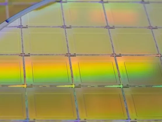
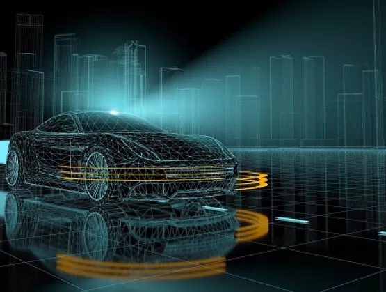
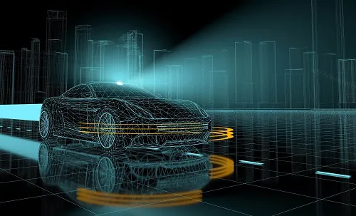
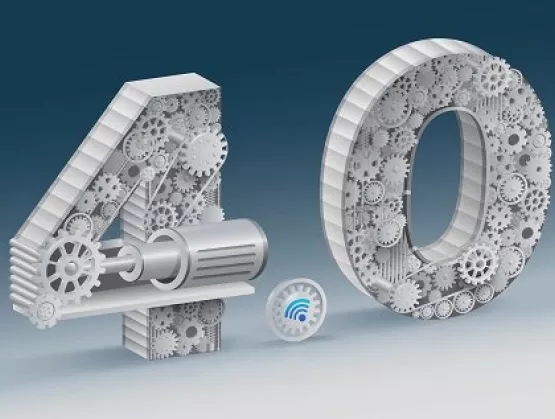
Connectivity. Electrification. Shared Mobility. Autonomous Driving. McKinsey Company cites these four disruptive trends behind future mobility — dynamics that could help to transform quality of life for hundreds of millions of people.McKinsey Company predicts that by 2030, mobility innovation could dynamically alter everything from safety in human locomotion to air quality, public spaces and power systems. Much the same way that tiny plankton in our oceans sustain aquatic animals, MEMS and sensors, while small, are crucial building blocks of integrated mobility.As partner at McKinsey Company, Andreas Breiter will explore this connection during his MSEC 2020 presentation, Future Mobility Enabled by Sensorization. SEMI recently caught up with Breiter to preview his October 7 talk at SEMI’s first virtual MEMS Sensors Executive Congress, October 6-8 and 13-15, 2020.Register now for MSEC 2020 and explore this topic with Breiter during the live Q A portion of his presentation.SEMI: You play a dual role at McKinsey Company, advising clients in advanced industries on capital investments and serving on the leadership team of the McKinsey Center for Future Mobility (MCFM). What is the relationship between them?Breiter: Mobility has become so much more than the auto sector. Today when we say future mobility, we’re talking about the convergence of many exciting developments influencing the ways that people and goods move around. Cars have become computers, and we now have to contemplate new frontiers, such as air taxis and electric vehicle infrastructure.Mobility is changing so quickly that it’s inspiring decision-makers from other market sectors to explore what implications it will have for them. We’re helping mining companies think about their haulers, retailers think about their footprints, and insurance companies plan for autonomous vehicles. The MCFM exists as a global think tank to focus on these frontier topics, helping to ensure we are ready for the future. During my MSEC presentation, I’ll explore how those future topics are influencing automotive mobility in the short- and long-term. The MCFM is even more forward-looking, so we’re just starting to build scenarios for what might come in 2040 and beyond.SEMI: How are changes in the mobility ecosystem affecting the automotive value chain?Breiter: In the past, the automotive value chain was clearly structured. We had sensor companies selling to Tier 1 suppliers, who would in turn sell to OEMs, who would sell directly to end customers.The value chain has grown more complex, however. In the future, we might see fleets of robotaxis, which will be owned by companies instead of by individual consumers. Already today, rideshare companies are game-changers because consumers can travel by car without owning one.Plus we see companies offer parts of the user experience such as user interfaces for automotive infotainment. In the past, everything in the car was branded by the OEM, but now we have third-party platforms that let us control some of our automotive infotainment options.SEMI: How are MEMS and sensors suppliers participating in this new value chain?Breiter: The pervasive use of sensors in cars has driven automotive OEMs and Tier 1 suppliers to work directly with suppliers, whose close involvement eases the complexity of integration. Just think about the sensors used in autonomous driving. Getting that right is safety-critical.We’re also seeing suppliers go beyond the individual component level to provide complete systems-level solutions. Advanced driver-assistance systems (ADAS) are a good example.SEMI: Automotive applications tends to have some of the longest design-to-delivery cycles in industry. Will this ever change?Breiter: The automotive product lifecycle was typically five-plus years, with a few years of development before that and continued service after the end of the lifecycle. That gives MEMS and sensors suppliers a 10+ year timeline on one model.With so much innovation taking place, this slow cycle won’t work forever. Over-the-air (OTA) updates, for example, enable new features when they become ready for deployment. I expect we’ll see OTA updates from many end manufacturers in coming years. SEMI: What changes do you foresee in ADAS and autonomous driving?Breiter: ADAS and autonomous features will become much more common. We’ve already witnessed this progression, with introductions first in premier models and later rolling out in more affordable vehicles. Lane-change assist and rear camera followed this path and are now pretty standard. Collision avoidance, as a safety-critical feature, is likely next in line for more widespread adoption.As for fully autonomous driving, consumers will accept that only when it becomes safer than a human driving a car.SEMI: Where is the greatest opportunity in the next five years?Breiter: Electrification of vehicles is number one. When it comes to engines, we’re moving from internal combustion to hybrid and then to electric. Since OEMs are adding sensors for the battery system, for battery management, and for electric motors, this progression represents growth opportunity for sensors suppliers – in particular for hybrid vehicles that contain both powertrain technologies.But that’s not all when it comes to sensors. Outside of powertrains, new sensors are added to enable a variety of functions, including, for example, ADAS and autonomy, as well as increased interior content, such as mood lighting.SEMI: Is there anything surprising coming, sensor-wise, in mobility?Breiter: To enable intelligent traffic systems, you need to make infrastructure smarter — which brings us to sensors. We’re going to see roads and other assets in infrastructure sense the state of traffic, sense what traffic participants are doing, and support connectivity between, for example, the infrastructure, vehicles on the ground, pedestrians on walkways and drones in the air.SEMI: What would you like MSEC attendees to take away from your presentation?Breiter: We’re living in a transformative era for the mobility industry. During the last 100 years of mobility, the ecosystem barely changed. In recent years, however, we’ve seen massive technological gains, largely enabled by semiconductors, MEMS and sensors. Instead of serving as just one of many suppliers, I’d encourage MSEC attendees to anticipate future mobility challenges so they can offer solutions to OEMs and Tier 1 suppliers accordingly.For more information, visit McKinsey Center for Future Mobility. MEMS Sensors Industry Group® (MSIG), a SEMI technology community that connects the MEMS and sensors supply network in established and emerging markets, enables members to grow and prosper. Visit us today.Andreas Breiter leads McKinsey’s capital-investment work for advanced industries in North America as well as its Center for Future Mobility on the West Coast. In his advisory work, Breiter serves a broad range of companies in the automotive sector, including car and truck manufacturers and their suppliers, as well as companies in the utilities and renewables space. He helps executives make strategic choices around product development and helps companies stay ahead of emerging trends, such as autonomous driving, connectivity, electric vehicles, and shared mobility.Andreas holds a Ph.D. in Operations Management and studied in Germany, France, the U.S. and Canada.Nishita Rao is product marketing manager at SEMI.
Read More
At the 1964 New York World’s Fair, Walt Disney and his team of Imagineers debuted Audio-Animatronics® in four attractions, Great Moments with Mr. Lincoln, General Electric Carousel of Progress, Ford Magic Skyway, and it’s a small world. As “a new type of animation” that Walt said was “so lifelike that you might find it hard to believe,” Audio-Animatronics captivated audiences, setting the stage for the technological innovation that would transform theme-park attractions for decades to come. While the Audio-Animatronics in classic Disney® attractions such as Enchanted Tiki Room and Pirates of the Caribbean® continue to delight park-goers, more modern attractions take full advantage of the miniaturized, sensitive enabling hardware components, software algorithms, and connectivity technologies that are available to today’s engineers.When Michael Tschanz, director of engineering technology and analysis, a segment within Disney Parks, Experiences and Products’ Global Engineering and Technology department, gives the opening keynote at MSEC 2020, SEMI’s first virtual MEMS Sensors Executive Congress (October 6-8 and 13-15, 2020), attendees will get a rare look inside the magic of select Walt Disney World attractions. Join MEMS Sensors Industry Group and SEMI on October 6 for Tschanz’s keynote presentation, Model-Based Design and Scientific Data Analytics of Disney Attractions — and experience video footage that you won’t see anywhere else. Register now for MSEC 2020.MEMS Sensors Industry Group® (MSIG), a SEMI technology community that connects the MEMS and sensors supply network in established and emerging markets, enables members to grow and prosper. Visit us today.In his role at Disney, Michael Tschanz leads a multidiscipline team which develops detailed mathematical and physics models for transportation, ride and animatronic systems, custom software and network applications, and robotics. The responsibilities for this team also include the development of optimization algorithms, servo controllers, interactive/immersive experiences, data analytics, and material process solutions. Michael’s rich and diverse background includes designs of numerous attractions at various Disney theme parks including: Test Track® Attraction; Mission: SPACE® Attraction; Toy Story Mania!® Attraction and the Expedition Everest® Attraction. Michael also designed all the velocity profiles at the worldwide locations of The Twilight Zone Tower of Terror™.Nishita Rao is product marketing manager at SEMI.
Read More