downloadGroupGroupnoun_press release_995423_000000 copyGroupnoun_Feed_96767_000000Group 19noun_pictures_1817522_000000Member company iconResource item iconStore item iconGroup 19Group 19noun_Photo_2085192_000000 Copynoun_presentation_2096081_000000Group 19Group Copy 7noun_webinar_692730_000000Path
Skip to main content
Default Banner Image

Technology and Trends

Machine learning (ML) and artificial intelligence (AI) have ushered in tremendous opportunities for faster growth, problem-solving and technological development in the electronic system design ecosystem. Cadence Design Systems, Inc., a member of the ESD Alliance, a SEMI Technology Community, is at the technological forefront in incorporating ML techniques in its chip design products. I spoke with Chin-Chi Teng, Senior Vice President and General Manager of Cadence’s Digital Signoff Group, about how ML is reshaping EDA and the semiconductor industry, the cloud’s role in the evolution of ML in design and its impact on Moore’s Law. Teng also offers advice on how engineering students can calibrate their education to prepare to work with this transformative technology and urges them to have fun in the process. Smith: How is ML changing the EDA industry? Teng: ML is changing EDA for the better in many ways. It’s more difficult than ever to design chips, and ML is helping by overcoming the complexity, size and technology interdependencies. At the same time, ML is helping our own engineers solve certain classes of EDA algorithm, tool, and flow/solution challenges so that we can deliver even better EDA tools to our user base. The benefits can include reducing runtime, increasing quality of results, and being better equipped to manage vast complexity and data. Also, and maybe even more significant, is the potential boost to user and team productivity, where engineers have more time to focus on high-value problems because they no longer need to spend time on managing overwhelming volumes of data and details that can be easily automated. Smith: What is the potential impact ML can have on semiconductor design? Teng: ML technology can be leveraged in several ways to improve EDA tool performance and engineering team productivity. For example, we initially applied ML to applications such as formal verification, simulation regressions, analog circuit design, and PCB design. We targeted ML toward specific algorithms that processed lots of data to sharpen and speed decision-making. Then we started to look at digital implementation flows that combine multiple steps with multiple decisions in a recipe, especially for chip implementation where the more efficient use of engineering knowledge can make a substantial difference in the chip’s resulting power, performance and area (PPA). These flows present more challenges and require different ML and optimization techniques since the data points are expensive to create and the volume of data is huge. But flow optimization offers the largest rewards for companies investing in data collection and analysis to improve their operations and product quality. By using ML to improve the implementation flow, our users are seeing up to 20% better PPA and 10x improved productivity in developing data center CPUs and AI engines, automotive sensor processing SoCs, and mobile devices. Smith: What is the cloud’s role in the evolution of ML in EDA? Teng: More ML usage means there will be an inevitable surge in compute demand resources, and engineers need the ability to scale in parallel. The cloud provides engineers with the best opportunity to scale computing resources without facing procurement limitations. The cloud also allows engineers to use task-specific compute and ML accelerators and capitalize on distributed computing innovations that leverage the cloud for greater design flexibility and availability. Smith: You have written that you see Moore’s Law accelerating. How does ML fit into this? Teng: We see the rapid adoption of new process technologies as the biggest trend surrounding Moore’s Law right now. ML technology in EDA will help speed tool certification processes, process design kit (PDK) development and other deliverables aimed at creating and improving customer support through all stages of the process lifecycle. This is a virtuous circle, and it’s expanding beyond hardware design and optimization to also include software. Today’s ML functionality works on the abstraction of register transfer level (RTL), optimizing the implementation and verification flows. ML will soon enable use of a higher abstraction of describing the target systems, exploring architectural options and optimizing across hardware and software partitioning. Smith: What advice would you give engineering students who are studying ML with the goal of becoming an electrical engineer? Teng: With the rapid pace of technology development, things are changing constantly. I’d absolutely encourage students to look at ML because ML isn’t going away — its growth is only going to accelerate from here. I’d also suggest that students look more broadly at computational mathematics because that’s foundational for ML. There are many, many opportunities to apply ML to real-world applications that will make a significant impact when it comes to optimizing computational software. Most important, students should explore and have fun while doing it. About Chin-Chi Teng Chin-Chi Teng has served as Senior Vice President and General Manager of the Digital and Signoff Group (DSG) since 2018. Prior to this role, Teng held senior leadership positions in research and development in digital implementation. Teng joined Cadence in 2002 via the acquisition of Silicon Perspective Corporation and subsequently led various research and development groups. He brought deep technical knowledge and more than 20 years of industry and academic experience to his role as leader of the IC Digital group. Teng holds a BS in electrical engineering from the National Taiwan University and an MS and Ph.D. in electrical and computer engineering from the University of Illinois at Urbana-Champaign. He holds seven patents and has written many EDA papers, several deep learning papers, and the book Electrothermal Analysis of VLSI Systems. Robert (Bob) Smith is executive director of the ESD Alliance, a SEMI Technology Community.
Read More
Three-dimensional integrated circuits (3D-ICs) are revolutionizing the semiconductor industry. Manufactured by stacking and interconnecting dies so they perform as a single device, 3D-ICs deliver more capabilities by offering higher performance and bandwidth — while also reducing power consumption, package size and costs. However, 3D-ICs present tough design challenges to engineers. Significantly larger than a single-chip system on a chip (SoC), these assemblies have more components, more integration points and longer interconnects, that translate to new risks for high-frequency signal failure, reliability, and other performance issues such as thermal buildup. As the lines between silicon and system continue to blur, engineers must conduct concurrent, multivariate analysis to assess every possible failure mode ― not only at the component level, but also across the entire 3D-IC assembly ― a technical obstacle for many development teams accustomed to applying a series of single-physics engineering simulation tools in a sequential approach. 3D-ICs are assembled in a complex package using a serial analysis approach that doesn’t take into account system-level interactions, as well as the many thousands of bump connection points where something can go wrong. By contrast, concurrent, multivariate simulation and analysis takes into account all physics simultaneously from the earliest prototyping stages of design. Most semiconductor development teams not only lack the technical tools to perform this complex simulation and analysis, but they also face cultural obstacles as they undertake system-level analysis. Diverse teams working with disparate tools simply aren’t equipped to perform seamless handoffs and collaborate effectively on a complex 3D IC design from an early stage. Instead, they scramble to address system-level issues later when launch delays are likely, the cost of rework is high and their positive contributions to the design are diminished. The Value of a True Multiphysics, Multivariate Approach As market demand for 3D-ICs increases, semiconductor development teams need a single simulation platform that enables simultaneous multiphysics analysis — including power integrity, reliability, electromagnetics (EM), thermal, computational fluid dynamics (CFD) and mechanical studies ― across the entire assembly. A unified simulation platform that brings together best-in-class solutions for every physics enables semiconductor engineers to collaborate across functions, seamlessly hand off analysis tasks between engines, and partner to optimize 3D-IC designs across every performance parameter. Costly surprises from signal integrity to thermal conductivity and structural strength are far less likely when the team reaches physical assembly to help ensure on-time, cost-effective product launches. An example of simultaneous multivariate analysis of a chip stack showing both thermal gradients and mechanical stress/warpage of the package at an early prototyping stage. By contrast, applying multiple physics sequentially can lead to ongoing and expensive setbacks. For example, as one team resolves signal integrity issues, another team could discover that timing failures or thermal risks have arisen. It’s not only back to the drawing board, but back to a series of time- and resource-intensive handoffs across disconnected simulation and analysis tools, as well as across functional boundaries. The Importance of Considering Novel Physics Because the pressure is on to launch innovative 3D-IC designs rapidly, development teams might be tempted to focus on existing signoff metrics ― which are complicated enough, across today’s multi-die assemblies — but overlook the application of more novel physics. This is a mistake that can result in failures in the field, product recalls, warranty expenses and lasting damage to the brand reputation. To achieve full product confidence across the entire 3D-IC system, semi engineering teams need a solution set and associated best practices that make it fast and intuitive to not only optimize performance and cost, but to concurrently analyze novel physics that will impact electrical reliability, mechanical stability and thermal failure modes. The number of physical effects that need careful simulation has risen in lockstep with Moore’s Law and has increased even more for 3D-IC design. The use of a single, connected platform enables this kind of true multiphysics analysis. A multiphysics platform should interface with popular design systems, and be extensible by Python API's to the user and to other vendors. For example, engineers can check the thermal behavior and the likelihood of melting and local failures of each solder bump based on the electrical current it carries. The engineers can apply computational fluid dynamics to evaluate how well airflows generated by fans and heat sinks work to cool down the assembly. They can maximize system reliability by examining unfamiliar effects like low-frequency power oscillations on the distributed power supply network. Best of all, a unified and purpose-built simulation platform enables semiconductor development teams to conduct all these studies simultaneously to rapidly reveal design trade-offs that arise when many elements are brought together in a complex assembly. Only this type of multiphysics, multivariate, concurrent approach enables engineering teams to reach all their goals for speed, confidence, innovation and product performance as 3D-IC designs take over the global market. Supporting a Culture of Vertical Integration Global leaders in the semiconductor and electronics industries benefit from a culture and organizational model based on vertical integration, which supports high levels of design collaboration. It can be tough for horizontally integrated, smaller companies to establish this depth of collaboration. Customers require open and extensible platforms that support a broad range of analysis tools across many different abstraction levels – from device to chip to board to system. The right simulation technology platform can significantly help. A shared platform that brings cross-functional engineering teams together for simultaneous, not sequential, multiphysics design can make it easy and seamless to collaborate across functional boundaries and support excellence in every aspect of power, performance, reliability and cost. By balancing these foundational performance aspects with simultaneous optimizations of temperature, mechanical stress and other subtle effects, semiconductor engineering teams can position themselves as leaders, not followers, in the 3D-IC revolution. Learn More at the Ansys IDEAS Digital Forum Register for Ansys IDEAS Digital Forum on demand to learn more about 3D-IC best practices from leading industry experts (www.ansys.com/ideas). John Lee is General Manager of the Electronics and Semiconductor Business Unit at Ansys.
Read More
In the early 1990s, engineers of varying degrees of skill with a powerful PC set up shop designing and selling blocks or libraries of reusable components with a defined interface and behavior. These blocks, known as intellectual property, or IP, were then (and still are) integrated into a larger design. While the new market segment created excitement and new opportunities, it also was untested and created uncertainty. Many fledgling companies failed. It’s a different story today. Arm, as well as Cadence and Synopsys, are silicon IP suppliers and the segment’s yearly revenue tops $4 billion, a long way from those early garage startup days. ESD Alliance member CAST, a silicon IP provider since 1993, participated in the remarkable growth and impact on the semiconductor industry. Nikos Zervas, CAST’s CEO, and I discuss those early days of the IP business and what’s ahead. Smith: What were the early days of silicon IP like? Zervas: In those early Wild West days of IP, vendors and customers both wanted to benefit from IP, but nothing was standardized, and people just tried things to see if they worked. The perceived barrier to entry was low: hundreds of IP companies sprang up thinking they only needed RTL coding skills and tools, an FPGA to prototype, and a few thousand dollars to invest. IP deliverables, quality standards, and business practices varied from vendor to vendor and over time. Risk was high, and there are many horror stories of re-spins or market failures due to faulty IP cores. Smith: How has the silicon IP market changed from its early days? Zervas: Firms delivering high-quality IP and providing outstanding customer support survived. Others disappeared. Eventually the industry centered around a reasonably common sense of IP requirements and quality and a consistent set of business practices. IP product complexity has driven upwards as SoCs have grown. The largest ASICs used to approach a few million gates; today they’re hundreds of millions, and the granularity of IP has evolved from small functions to pre-integrated subsystems. Early on, a designer doing image processing might license individual functions like a Finite Impulse Response (FIR) filter or a Discrete Cosine Transfer (DCT) block. Today, instead they would license a complete JPEG compression core containing those functions and more, or even a complete black box subsystem streaming processed, stabilized, compressed video over Ethernet. IP selection criteria have also changed. Early IP was handcrafted to eliminate every extra gate, as being a few thousand gates smaller was a killer advantage in the era of 180nm ASIC processes. Today, at 7nm or 5nm process, tens of thousands gate differences are just noise, and it’s usually the reliability, functionality, and performance of an IP core that matter most. Smith: When did the silicon IP market start to take off? What was the driving force? Zervas: By the early to mid 2000s, uncertainty about what IP was and how best to use it – and the early wave of less-than-great providers – were being replaced by increasing acceptance and emerging best practices. The introduction of smartphones, the wild growth of Internet of Things applications, growing automotive system sophistication, and other advances fueled the explosion of the IP market in the late 2000s. In fact, according to the ESD Alliance Electronic Design Market Data Report, revenue from IP licensing today has surpassed the license revenue from front-end EDA tools. This would have been unimaginable in the late 1990s. Smith: How has silicon IP changed chip design? Zervas: Designers today must develop massive, complex systems with an even tighter time to market. Only the higher level of design abstraction and the distributed expertise that silicon IP provides make this possible. But IP also increases the challenge of differentiation: With the same IP available to everyone, how do you design a product that stands out in its market? The answer to differentiation today lies mainly in clever SoC architecture. Delivering better features with superior performance, lower power consumption, or other winning characteristics now depends not so much on perfecting each separate IP block but rather from selecting the best IP for the system’s requirements, integrating those IP cores for clean communication and efficient resource sharing, and other smart system-level decisions. It’s similar to modern building design: Every firm has access to the same materials and tools – concrete, glass, etc. – but only a few produce exceptional buildings. Smith: It seems that are several different business models for IP licensing, such as up-front license fees, subscriptions, royalties, or a combination of these. Do you think the IP market will gradually align around one basic model, or will it continue as is with a variety? Zervas: Different models serve different needs. For example, commodity IP like a SPI interface can’t demand royalties, but unique, leading-edge IP – like a 112Gbps SERDES – still can. I believe the market will continue with different business models, though the number of different models may shrink and their terms begin to align. About Nikos Zervas Dr. Nikos Zervas is the chief executive officer of CAST, Inc. He co-founded image and video compression IP developer Alma Technologies in 2001, and led the bootstrapped firm as chairman and CEO for nine years before joining CAST. He was a founding member of the Hellenic Semiconductor Industry Association and served on its board for several years with responsibility for strategic planning. He is a senior IEEE member and member of the Technical Chambers of Greece, had contributed to the GSIA's IP Working Group, and has published multiple technical papers on data compression design and related topics. Robert (Bob) Smith is executive director of the ESD Alliance, a SEMI Technology Community.
Read More
Alameda, Calif.-based Verific Design Automation, a member of the ESD Alliance, made its name in the electronic system design and semiconductor industry supporting companies ranging from startups to billion-dollar industry leaders such as Synopsys, Cadence, Siemens EDA, Xilinx, Microchip, NVidia, Infineon, Qualcomm, Renesas and Samsung. Its software is used as the front end to design automation tools such as synthesis, simulation, debug, and formal verification. I spoke with Verific president and COO Michiel Ligthart about homegrown and open-source EDA tools and other recent trends in chip design. Smith: What trends are you seeing in chip design? Ligthart: Semiconductor companies are starting to build a portfolio of intellectual property, including homegrown electronic design automation (EDA) tools, that they want to keep secure and differentiated from their competitors. The increased interest in internally developed and supported EDA tools is a trend we started to see about two years ago. It’s not simulation, synthesis or place and route (P R). Instead, it’s pieces of a chip design flow optimized for a company’s specific needs. In the past, a semiconductor company would either standardize on one EDA company’s chip design flow or mix and match best-in-class tools from different vendors. The common denominator was that they used off-the-shelf products. If they had a specific requirement, they went to the EDA provider for assistance. In today’s competitive landscape, semiconductor companies are figuring out ways to diversify themselves and their design flow became a way to do so. They may not build their own P R tool, but they will look at building their own power domain approach, for example. Is this a widespread trend? It could be. We hear about it within end-user applications ranging from 5G and AI to data center processors and there are probably others we don’t hear about. Power optimization is an example of the kind of specific internal need being addressed. Smith: What are your thoughts about open-source EDA tools? Ligthart: Our industry supports open source already with language reference manuals (LRMs) for VHDL, SystemVerilog, Unified Power Format (UPF) and the RISC-V Instruction Set. The LRMs and the instruction set are free. Moving to the development of actual tools becomes a question of who will implement, support and maintain the tools. Implementation is expensive. The Big Three (Cadence, Siemens EDA and Synopsys) invest about 35 to 40% of top-line revenue into R D. For smaller EDA companies, this number is even higher. The industry may come up with a business model that will have open-source components as well as a way to fairly reimburse companies that make these tools freely available. I have not seen it yet. Smith: Business Insider reports that Verilog HDL is among the top 10 tech skills that companies are desperate for their employees to learn right. Does Verific get asked about Verilog training? Ligthart: No. Our customers are experienced users. Nonetheless, it was great to read that article and it suggests the semiconductor industry is healthy, growing and hiring talented engineers. Smith: If an entrepreneur asked you for advice about starting an EDA or IP company, what advice would you provide? Ligthart: I would tell the entrepreneur to focus on the problem the startup is solving. Stick to the company’s core competency and try not to build in-house what can be purchased from a reputable supplier. In the end, it will save time and jump-start the development effort, and the engineering budget can be allocated to the startup’s core competency. The external supplier presumably has years of product validation, which brings a major QA gain. About Michiel Ligthart Michiel Ligthart, president and COO of Verific Design Automation, has an extensive background in engineering, product marketing and general management. Prior to joining Verific, Ligthart was vice president and general manager of West Coast operations for Theseus Logic, a startup in asynchronous logic. Before that, he spent eight years with Exemplar Logic in engineering and marketing roles. Ligthart started his career with Philips Research Labs in California and was a visiting scholar at the Center for Integrated Systems at Stanford University. He has a Master of Science degree in Electrical Engineering from Delft University of Technology, the Netherlands. Robert (Bob) Smith is executive director of the ESD Alliance, a SEMI Technology Community.

Read More
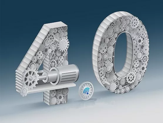
Demand for hi-tech manufactured goods is at an all-time high and is expected to grow significantly in our new digital age, COVID-19 economy. This is especially true for semiconductor chips. Chip manufacturers have been working to meet this demand by building new factories and by optimizing processes and equipment in existing fabs. While there is much media coverage about new factories planned by leading-edge chipmakers and government investments in the semiconductor sector, greenfield fabs entail significant capital expenditures and are sometimes fraught with complex political concerns. As a result, they can take several years to complete and reach their planned production capacity. Instead, the semiconductor industry needs to optimize existing factories in order to increase productivity and yield and meet growing demand by implementing smart manufacturing solutions. Smart manufacturing solutions will inherently reduce costs with more efficient and automated processes, and those savings can be reinvested for the next wave of solutions. Chip Industry on the Bleeding Edge Semiconductor manufacturers have always been focused on bleeding-edge technology to outflank strong competition and build the best products – faster and cheaper. Today, pioneering organizations are using data to optimize manufacturing processes and equipment, a practice known as Smart Manufacturing. While there are many definitions of Smart Manufacturing, the essence is maximizing the utility of big data generated in these factories by leveraging three pillars: Sensing, Connecting, and Predicting. It is not just the digitization in manufacturing, but it is also about turning the data into actions that generate value – an effort the SEMI Smart Manufacturing Committee is driving based on the three pillars. Optimizing return on investment is the ultimate goal. SEMI Smart Manufacturing Initiative activity is based on three pillars that support the goal of increasing ROI. Making the Right Decision, Faster Smart manufacturing practices enable organizations to make the right decisions and take action faster based on insights generated from real-time and historical data. This requires data management technologies and applications that can process, analyze, and act on information instantly. It has become ever more difficult to process and discern the relevant data or signal from the vast volume of data, perform analytics or develop new ML or AI analytic tools, and then make the critical decisions to solve problems as close to real-time as possible. Who’s Responsible – IT or OT? In the past IT (Information Technology) and OT (Operations Technology) were separate entities within organizations, with IT focused on storing large amounts of data for enterprise systems and OT concentrated on using data to perform specific functions. Smart Manufacturing often demands combining IT and OT, difficult in rigid organizations that operate the two organizations independently and lack the infrastructure to implement comprehensive solutions. Success requires executive leadership sponsorship, motivated technical personnel and, most importantly, a clear deliverable on the value in implementing Smart Manufacturing. Many organizations have introduced top-level leadership positions such as a Chief Information Officer or Chief Data and Analytics Officer to address this convergence and many of these leaders are embracing Smart Manufacturing practices. The SEMI Smart Manufacturing community includes many of these leaders and therefore has highlighted the importance in the return on investment for Smart Manufacturing solutions. Read more about IT and OT convergence and note that Smart Manufacturing is synonymous with Industry 4.0. The SEMI Smart Manufacturing Initiative covers the entire supply chain. Get Smart in Smart Manufacturing While new technologies and applications are being created to deal with mountains of data, it is the underlying methodologies and practices that are key to a successful Smart Manufacturing deployment. SEMI, the trade association representing the electronics manufacturing and design supply chain, is in a perfect position to evangelize Smart Manufacturing experiences and best practices for the entire manufacturing community. The more than 30 member companies participating in the SEMI Smart Manufacturing Initiative bring more than 500 years of collective experience and knowledge to the topic. Many segments of the supply chain participate in the SEMI Smart Manufacturing Initiative including packaging, assembly, SMT and PCB assembly, test, software, data management, sensor and material suppliers. Learn How to Manufacture Smarter SEMI SMART Manufacturing is hosting two great conferences in the coming months – the Global Smart Manufacturing Conference (GSMC) and the SEMICON West Smart Manufacturing Pavilion. As a leader of the organizing committee and chair for the SEMICON West Smart Manufacturing Pavilion, I encourage people who want to learn how to implement Smart Manufacturing or expand their knowledge of Smart Manufacturing to attend these events. The GSMC will feature keynotes highlighting the value of Smart Manufacturing, offer tutorials on the three pillars, and introduce several case studies for each of the pillars. Thirty-two organizations – ranging from global cloud providers, semiconductor factory operators, leading equipment vendors and software application solution companies – will present. See the full agenda here. The SEMICON West Smart Manufacturing Pavilion will compliment GSMC by showcasing a number of use cases that highlight the value of Smart Manufacturing. Panel discussions will deep dive into the challenges of implementing these best practices and the direction smart manufacturing is taking in the coming years. Our goal for these events is for you to take this knowledge back to your companies, implement and improve on the detailed solutions highlighted at the conferences, and return next year to share your success stories with the community. See you soon, in person or virtually! About the Author Bill Pierson is VP of Semiconductors and Manufacturing at KX, leading the growth of streaming data analytics in this vertical. Bill is also a chair for the SEMICON West Smart Manufacturing Conference and an active team member of the SEMI Americas Chapter. He has extensive experience in the semiconductor industry including previous experiences at Samsung, ASML and KLA. Bill specializes in applications, analytics, and control. He lives in Austin, Texas, and when not at work can be found on the rock-climbing cliffs or at his son’s soccer matches.
Read More
Areas packed with dense foliage. Mile-deep mines and tunnels. Urban canyons. Indoor environments. Global Positioning System (GPS) technology has long been a boon to location tracking of aerial, terrestrial and aquatic vehicles — as well as to people in motion — but in many cases it can’t function with a high degree of reliability, either because the GPS signal is somehow obstructed, or worse, is jammed or spoofed. Delivering higher precision and higher reliability in GPS-denied environments — as well as immunity to jamming and spoofing — positioning, navigation and timing (PNT) represents the next evolutionary step in location positioning and tracking. With PNT so critical to a range of defense, commercial and industrial applications — and with sensors the building blocks of PNT solutions —the MEMS Sensors Industry Group, a SEMI Technology Community, is ensuring that our members play a transformative role in PNT innovations. We’ve secured $14.9 million in research dollars for PNT R D over the past 18 months, marking Phase I of a project funded through a public-private consortium with the U.S. Army Research Laboratory (ARL). With the typical funding structured as a 50/50 cost share with the industry participant, the research dollars go farther, and the level of commitment that each recipient makes is more pronounced. As we look ahead to Phase II of the MSIG PNT R D project, the details of which we’ll announce later this year, we’d like to reflect on the companies and research labs that won bids through a competitive process supported by the SEMI-MSIG PNT Technical Advisory Council and the SEMI-MSIG PNT Governing Council. Winners submitted proposals that both met our criteria for advancing PNT technologies relative to mobility, size and weight, and that laid a path toward greater cost efficiency and lower product price. “PNT doesn’t displace GPS,” said Tim Brosnihan, executive director of SEMI-MSIG. “Rather, getting the two technologies to work together improves position and tracking. While current PNT solutions use inertial measurement units, or IMUs, to effectively maintain positioning accuracy in the absence of a GPS signal, it’s also true that accumulated bias and noise-related errors in the IMUs make positional determination unreliable. Like most great pairings, GPS and PNT can work together. We can use IMUs when GPS is unavailable, and when GPS returns, it can be used to reset the IMU errors. So when the GPS signal is lost again, the IMU can maintain navigation and location. “We’re focusing this PNT project on technologies that will allow accurate positional determination in the absence of a reliable GPS signal for prolonged periods,” added Brosnihan. Here are snapshots of the 10 companies and research institutions that won awards for their PNT-focused developments. Analog Devices is developing an optimal size, weight, power, and cost (SWaP-C) solution for applications requiring high-accuracy navigation and uncompromised reliability. The company’s mode-matched navigation-grade gyroscope with system ID leverages an innovative sensor and its associated process design, a robust high-volume manufacturing flow, and system-control algorithms to achieve very high-performance (0.01 degree/hour bias instability and 0.005 degree/√hr angle random walk). Carnegie Mellon University (CMU) is developing a CMOS MEMS high-stability accelerometer through machine learning (ML). If embedded in footwear, these ML-optimized accelerometers could be used in personal navigation. If embedded in a golf ball, baseball or hockey puck, the accelerometer could extract the trajectory of the object in motion by measuring its shock (force). The CMU device validates state-of-the-art performance of the university’s high-dynamic-range accelerometer systems-on-chip. It also validates and tests ML models by measuring the accelerometer and auxiliary sensor output over long time periods (e.g., 1 hour, 10 hours, days) to collect independent long-duration time-series data. By modeling drift from environmental influences — along with possible overall system changes from extreme events, such as high-temperature excursions and shock — designers can dramatically reduce navigation errors to support more accurate navigation over longer time periods. GE Research is developing a novel MEMS gyrocompass that will enable high-end north-finding systems, traditionally unaffordable for automotive and consumer applications. The device will be available in mass-market applications such as robotics and autonomous vehicle navigation in GPS-denied environments. The MEMS gyrocompass enables a 10x reduction in SWAP-C with high accuracy. An additional benefit of this work is that GE will offer a foundry service process development kit (PDK) for its Polaris MEMS process, speeding the development and manufacture of MEMS devices in an advanced processing facility. Georgia Institute of Technology is developing high-aspect-ratio monocrystalline silicon carbide-on-Insulator (SiCOI) MEMS devices that will reduce navigation angle errors, potentially making widescale pedestrian navigation available in mass-market applications such as smartwatches and smartphones. The platform for ultra-high-performance bulk acoustic wave (BAW) gyroscopes and timing resonators will feature material properties that allow a much better structural symmetry and a higher-resonant quality factor (Q) than silicon MEMS (Si MEMS). Honeywell is working to enhance the navigation accuracy of commercial and military vehicles in GPS-denied environments through an innovation that dramatically improves the performance of a MEMS IMU by both refining candidate ML algorithms, including recurrent neural networks (RNNs), and by combining deep neural network (DNN)-based calibration and sensor fusion algorithms. PARC is developing a new materials platform for photonic integrated circuits (PIC). Aluminum gallium nitride (AlGaN), an ultra-wide bandgap semiconductor, is epitaxially grown to produce single-crystal layers for fabrication of optical components, such as waveguides and micro-ring resonators for optical signal processing. The project includes design and fabrication of specialized laser diodes at wavelengths needed to probe qubits based on atomic ions (e.g., strontium and ytterbium). The new platform offers several benefits: low optical loss from the ultraviolet (UV) to infrared spectral bands excellent non-linear optical properties for efficient frequency-generation processes (e.g., optical frequency combs); and enabling technology to realize compact, field-deployable quantum systems for PNT applications, such as ultra-fast distance measurements, microcombs for optical atomic clocks, photonic radar, optical coherence tomography, and coherent communications — all applications that benefit from the lower cost and small chip size of these integrated photonic circuits By expanding its proprietary EpiSeal encapsulation process to include new materials and topologies, SiTime is developing low-impedance and low-noise MEMS resonators with an ultra-stable wafer-level package. Because these novel MEMS resonators are highly reliable and very compact — while using less power and providing lower RF noise — they’re ideal for 5G RF timing applications, IoT devices, and smart vehicles. Teledyne Scientific Imaging (CSAC project) is conducting a study to identify paths to reduce the cost of battery-operated chip scale atomic clocks (CSAC) that provide affordable precision timing for denied environments. The project goal is to identify viable paths of reducing cost by an order of magnitude, without sacrificing performance. In addition to exploring design and manufacturability solutions, project researchers are performing short loop experiments as proof-of-concept validation. Through a second award, Teledyne Scientific (IMU project) is advancing packaging and integration for compact, navigation-grade six degrees of freedom (DOF) MEMS IMUs. Featuring reduced bias instabilities associated with packaging stresses and ambient temperature influences, the Teledyne Scientific IMUs promote environmentally robust low-stress packaging of wafer-level vacuum packaged (WLVP) MEMS gyro resonators, facilitating a lower-cost, smaller and more accurate IMU for performance-driven PNT applications. Twinleaf is developing a new light source module ideally suited for integration directly into quantum sensors. This project integrates a bright, tunable distributed Bragg reflector (DBR) near infrared (IR) 795nm wavelength laser made by the project’s subcontractor (Photodigm) into a package that locks the laser to an atomic reference line in a microfabricated vapor cell. The laser module’s high-output intensity and low magnetic signature will enable breakthrough performance levels for Twinleaf’s magnetometer and other quantum sensors requiring the light source integrated into the sensor module. Request for Proposal for Phase II of SEMI-MSIG PNT Program Opens Q4 2021 SEMI-MSIG will accept request for proposal (RFP) submissions for Phase II of its PNT program starting in Q4 2021. This year, in addition to funding IMU and timing device projects, MSIG will also consider proposals on imaging-based navigation solutions. If you’d like to submit for Phase II, sign up to receive more information on the RFP by visiting SEMI’s R D Programs page. You can also connect with Paul Carey by email, [email protected] or LinkedIn. Paul Carey, Ph.D., is the director of the MEMS Sensors Industry Group. With deep domain expertise in X-ray imaging backplane platforms — and their supply-chain technologies such as flexible substrates, laser annealing for semiconductors and silicides, thin film transistors (TFT) for flexible OLED displays, and polysilicon-on-plastic TFT technology — Carey has held technical leadership positions at dpiX, Applied Materials, and Lawrence Livermore National Laboratory. He received a double-major B.S. from UC Berkeley in Electronical Engineering and Computer Science (EECS), and Materials Science and Engineering (MSE). Carey holds an M.S. in EECS from UC Berkeley and a Ph.D. in MSE from Stanford University.
Read More
As we round the corner on 2021, the microelectronics industry continues to face a severe talent crisis. With more than 34,000 jobs remaining unfilled at SEMI member companies in the United States alone, everyone is competing for the same talent pool. While the semiconductor shortage has received extensive media coverage, a critical talent shortage deserves equal attention. One way to address the talent shortage is to hold the line. Meaning, in addition to recruiting more diverse talent into the chip industry, we must retain the quality workforce we have. I believe that a key component of a diversity, equity and inclusion program must be retention. At Edwards, we feel so strongly about this that we have made retention a key part of our Diversity, Equity and Inclusion program – even changing the acronym to DEIR (pronounced DEER; diversity, equity, inclusion and retention) for emphasis. There are three overarching approaches we can take to promoting diversity-focused retention:Investment in on-boarding practices that allow time to hire appropriately and ensure a diverse pool of qualified candidatesEmbedded programming and policies that are learning and development (L D) based including career planning, succession planning, unconscious bias training, employee resource groups (ERG) and mentoringCorporate culture that respects employees through a healthy work life balance and promotes the well-being of society and the planetThis is a very important conversation. I asked Lubab Sheet-Davis, vice president of Strategy Innovation in the Office of the CTO at Lam Research, and Emerald Greig, executive vice president Americas at SurplusGLOBAL USA, to share their considerable experience and insight related to retention and DEI. Following is an excerpt from our conversation, which has been edited for clarity and brevity.Balaguer: In the context of DEI, why is employee retention so important?Sheet-Davis: In my view, there is a strong correlation between inclusion and retention. If people feel that their voices and perspectives are valued, they are more likely not only to stay, but also to perform at a higher level. Driving both inclusion and retention is having a seat at the table, having your voice heard, respectful treatment and fair opportunity. Retention is a core component of our inclusion and diversity strategy, which involves increasing representation by building a pipeline of diverse candidates, recruiting and retaining, fostering an inclusive culture (which supports retention) and open communication to share our progress.Balaguer: What role does data play in the drive to increase retention?Greig: Ours is a data-driven industry and I am surprised that we have not let the statistics drive us into action sooner. Clearly, diversity, equity, inclusion and retention all affect the bottom line. Millennials and Gen Zs already leave faster than any other generational group. The turnover rate in the tech industry averages around 13% with stays around 2-3 years.The cost to hire, train and integrate someone into a company is far more expensive than having a DEIR program in place to keep them. The Society for Human Resource Management (SHRM) reported that, on average, it costs a company 6 to 9 months of an employee's salary to replace them (which includes the costs of hiring, onboarding and training, L D and time to fill the role). For an employee making $60,000 per year, that comes out to $30,000 to $45,000 in recruiting and training costs.Sheet-Davis: Yes, which gives us all the more reason to move quickly! Given how central DEIR is to innovation, and that the challenges and opportunities facing our industry are bigger now than ever before, I believe we should be addressing DEIR with the same vigor that we address Moore’s Law.I worry if we keep saying DEIR will take time, it will take time. Granted many DEIR issues are cultural and culture is hard to change. However, this industry has demonstrated the capability to drive breakthroughs and to do so quickly. Let’s focus on DEIR with urgency while also ensuring the progress is sustainable.Balaguer: There is no doubt we need to move with a sense of urgency. I think a good way to keep the pedal to the metal is to create a DEIR roadmap that tracks our progress on multiple programs and helps us be accountable and stay focused. Meaningful retention strategies begin with solid diversity-focused hiring strategies.Balaguer: How does corporate culture inform retention?Greig: Let’s not forget: Employees, especially millennials, are looking for a corporate culture that demonstrates social responsibility as well as leadership and career development. In a recent study, 65% of employees said positive corporate culture has encouraged them to stay with their company. In fact, companies with strong cultures have seen a four-fold increase in revenue growth.We have raised a generation that strongly believes in being accepting of others and embraces equity and inclusion in their daily lives. They expect their employer to have this as part of their DNA. They believe in science, climate change, recycling, conservation, and similar sustainability issues and they want to know that they are making or doing something that makes the world a better place. If tech companies cannot convince millennials and Gen Z's that the companies are socially responsible and are doing all they can to embrace DEIR as part of their company culture, then the millennials will go elsewhere. Balaguer: How can employee resource groups be a building block for retention?Sheet-Davis: We support employee resource groups that are voluntary, employee-led and coalesce around demographic factors such as gender, ethnicity, sexual orientation or generation. Each has an executive sponsor, budget, plans and leadership structure. ERGs support inclusion by creating a sense of belonging, building comradery, and providing a safe space to raise awareness and help educate the rest of the company through a number of activities such as community service, holiday celebrations, guest speakers, networking, training courses and more. I serve as the executive sponsor of our Women@Fremont group, which is focused on accelerating the advancement of women in their early to mid-career at Lam’s headquarters. I know ERG members genuinely value the company’s support.Balaguer: What can we do during the hiring process to lay a strong foundation for employee retention?Greig: I believe that the work we do at the front end in terms of hiring practices are one of the main reasons we have a low turnover rate at SurplusGLOBAL. We have a policy to have three interviews for each candidate. Not three different people, but bring them in three times. Additionally, we have a 90-day trial and review period to make sure there is a good fit for both parties. Investing time up front ensures the right hire and the small size of our company allows us to know our employees. We can be nimble and quickly respond to employee needs as they arise.Balaguer: In what ways do you think mentoring can help improve retention?Sheet-Davis: Another aspect of building a more inclusive culture, and hence promoting retention, is through mentoring programs. Mentorship supports an employee’s development, growth and career planning. It’s a great way to get to know people, understand their ambitions and support their development. Hopefully, it results in sponsorship because that is what helps drive career advancement. Ultimately, I want to advocate for those that I mentor.Balaguer: At Edwards, we are refreshing mentoring as part of our DEIR program. I see mentoring as a program that can support employee retention in multiple ways including career planning, professional development, succession planning and promoting inclusivity. Encouraging and empowering personal development is key in growing a productive workforce and mentoring does all these things. Often overlooked is the fact that mentoring is a benefit to both the mentor and the mentee. I have personally mentored several young professionals at Edwards, and I can attest that I have learned as much from them as they have from me. Mentoring is definitely a two-way street.Balaguer: What’s your message to our readers about retention as an element of diversity, equity and inclusion?Greig: I am excited to see DEIR and especially, retention, gaining traction. The semiconductor industry has always tended to have a cyclical rhythm to it. A generation of potential employees have grown up witnessing the fallout from periodic down cycles and the inevitable reductions in workforce. I think there is an element of rebranding we need to do in this area to support our retention efforts. Sheet-Davis: If we only focus on recruiting and not retention, we tread water. Consistent with any other successful business strategy, a holistic integrated approach to DEIR that is prioritized, resourced and sustained over time is key. Balaguer: We all agree that retention is a key component in the war for talent. While this conversation has been more wide-ranging than we can share with our readers, the prime takeaways have focused on these elements: Follow the data. Execute with a sense of urgency. Hire right. Work hard on inclusionary programming such as ERGs, mentoring and sponsorship. Build a genuine corporate social responsibility program. Retention will result.Many thanks to Lubab Sheet-Davis and Emerald Greig. As always, comments, questions and suggestions are welcome. We can be reached at [email protected], [email protected] and [email protected]. I invite our readers to join the conversation, as well as review the recently released SEMI Foundation DEI Roadmap and Toolkit.Scott Balaguer is Vice President and General Manager, Semiconductor Division at Edwards Vacuum LLC and Chairman of the SEMI North America Advisory Board.
Read More
Throughout the current millennium, System-on-Chip (SoC) has been the gold standard for optimizing performance and cost of complete electronic systems. By incorporating practically all the phone’s digital plus analog capabilities onto a single, giant chip, the mobile phone processor serves as a near-perfect exemplar of SoC. But today’s leading integrated circuits (IC) are pushing up against the upper limit of a chip’s size which is limited by the manufacturing equipment’s optical reticle size. This has proven difficult to increase and has grown only slowly over the years. Yet market pressure continues unabated for bigger, more capable electronic systems with more integrated memory, more digital logic, and more analog/mixed signal circuitry. An emerging solution to this tension is 3D and 2.5D multi-die chip assemblies – often referred to as 3D-IC. The key technology breakthrough of 3D-IC is that it makes it possible to spread a system out over multiple, smaller chips that are then assembled close together and interconnected with high-speed, low-power interconnect technologies. By abandoning the need to integrate an entire system on a single SoC and instead allowing it to be disaggregated over multiple chips, 3D-IC enables Moore’s Law to break through the reticle size barrier, improves yield by shrinking the size of individual chips, and makes it possible to mix different process technologies optimized for each function. The Four Engines Driving Semiconductor Design The road forward is not without its challenges, however, and we are seeing design companies making significant efforts to adapt and come to grips with the following four technology and market drivers: The requirement for concurrent multiphysics analysis to ensure reliable and efficient electronic systems The blurring of the lines between silicon and system The need for open and inclusive multiphysics platforms that interoperate with the multitude of design platforms The need for, and value of, bespoke silicon for hyperscalers and system companies Blurring of Silicon and System Design The advent of 3D-IC opens up new horizons for solutions that can be implemented in silicon. But it also forces a closer integration between two distinct technology markets that have co-existed symbiotically for many decades: IC design and printed circuit board (PCB) design. These markets use different tools, different data formats, different manufacturing back-ends, operate at different computational and geometric scales, and focus on different physical concerns. Yet, 3D-ICs share many aspects of both markets: They include monolithic chips but also board-like substrates to stitch the chips together. And in between the two disciplines is packaging, a completely different domain that is requiring companies to re-imagine their design capabilities and flows, as well as their organizational structure. Open, Extensible Multiphysics Platforms The siloed isolation of chip design from PCB design and package design means that each of these markets has developed insular data structures that are ill-suited to deal with the breadth of multiphysics analysis for 3D-IC design. Many different physical disciplines, including computational fluid dynamics, mechanical stress, and electromagnetic radiation, all need to work together based on open and extensible multiphysics platforms. These platforms must embrace the modern cloud compute paradigm and enable an ecosystem by allowing individual design platforms to connect for comprehensive multiphysics analysis. Bespoke Chips Today’s market-leading companies are heavily dependent on technology for their continued success and market differentiation. Everybody from online retailers to telecommunications to social networking companies and hyperscalers are moving away from off-the-shelf solutions and turning to custom-built silicon to give them an edge. Many of these companies are seeking to gain market share by leveraging proprietary AI/ML algorithms trained on their extensive troves of market data – but this requires huge amounts of compute power and specialized chips. Access to high-quality silicon solutions is vital in today’s world and the demand is for continually more complex and powerful electronics. 3D-IC an Inflection Point in Electronic Design To be sure, 3D-IC design is at an inflection point in electronic design and presents major challenges that are realigning the electronic design industry around this new reality. For more insights on this topic from a semiconductor industry leader, please view the Keynote Address 2.5D and 3D – The Road Ahead by Vicki Mitchell, VP Engineering, Arm Central Engineering Systems Group presented at the latest Ansys IDEAS Forum. And for an EDA perspective, please view Successful 2.5D and 3D Multi-die Silicon System Design Using Synopsys’ 3DIC Compiler and Ansys’ Multiphysics Analysis from Synopsys SNUG World 2021. About John Lee John Lee is general manager and vice president of the Ansys Electronics and Semiconductor Business Unit. Lee co-founded and served as CEO of Gear Design Solutions (now Ansys), developer of the first purpose-built big data platform for integrated circuit design. He cofounded two other startups (Mojave Design and Performance Signal Integrity), which successfully exited into companies now part of Synopsys. He holds undergraduate and graduate degrees from Carnegie Mellon University.
Read More
AEM Holdings Ltd, a Singapore-based multinational corporation, is listed in Forbes Asia’s 200 Best Under A Billion 2019 and 2020 spotlighting small and midsized companies in the Asia-Pacific region with sales under $1 billion. AEM clinched the Singapore Business Review Technology Excellence Award 2020 for Analytics-Semiconductor and the Singapore Business Awards Enterprise Award 2019/2020. These achievements are testament to AEM’s vision and innovation and the company’s contributions to the increasingly complex testing of chips in a rapidly evolving technological world. I spoke with AEM CEO Chandran Nair, a new Regional Advisory Board (RAB) member of SEMI Southeast Asia, about the company’s intelligent test and handling solutions, its role in digital transformation, the company’s key role in the smart manufacturing movement and the growth prospects for Singapore’s electronics sector. SEMI: AEM’s application-specific, intelligent system test and handling solutions for semiconductor and electronics companies serve the advanced computing, 5G and AI markets. How do you differentiate your solutions from those offered by competitors? Nair: A key differentiation for AEM is that we work closely with our customers to develop application-specific integrated test and handling solutions that meet their needs in a scalable manner from lab to production. We offer our customers customized, full-stack test and handling solutions that give them the agility to accelerate their delivery cycles and enhance product quality. Over the years, AEM has developed and acquired world-class technologies in instrumentation, test, automation, robotics, optical inspection, high-end thermal control, and software. These technology pillars, along with our deep know-how to customize test and handling solutions using the technology pillars as a platform, enable AEM to meet the fast-changing needs of our customers faced with the challenges of testing heterogeneous and complex devices. In addition to investing in technology, AEM has also invested in delivering application-specific solutions to meet customer demand. Our recently announced acquisition of CEI with its manufacturing capabilities in Vietnam and its specialization in low-volume, high-mix manufacturing increases our geographical reach and our ability to quickly turn application-specific test and handling solutions to be deployed. We have a unique and differentiated approach that enables our customers to test high-performance computing devices, automotive devices, and mobility devices with maximum test coverage, cost-effectively, in a manufacturing environment. Our experience in serving the high-performance computing market that traditionally drives advancements in thermal control also puts us at the forefront of delivering comprehensive thermal management, vision, and deep automation and test solutions for the computing, automotive, and mobility markets. AEM also has a strong instrumentation portfolio, including high-density digital instruments and mixed-signal and protocol-aware instrumentation that is well-suited for ATE solutions for SoC, high-power devices, and CMOS image sensors. Over the last few years, we have also established leadership positions in developing and deploying application-specific test solutions for MEMS devices and offering wafer and frame probing stations suitable for R D, wafer sort, and final test. We form strong partnerships with our customers, provide them with end-to-end support in product development, and take them through the entire life cycle process from concept to mass production. Chandran Nair and Goh Meng Klang, vice president of operations, at the AEM manufacturing site in Singapore. (Photo credit: AEM) SEMI: Digital transformation is powering strong growth of advanced computing, 5G and AI. Will AEM be expanding its AEM manufacturing plants in China, Malaysia and Singapore to meet rising demand for these technologies in the coming years? Nair: In regards to manufacturing, AEM currently has manufacturing facilities in Singapore, Malaysia, the U.S., Finland, and China. With our recently announced acquisition of CEI, we will add manufacturing capability in Vietnam and Indonesia. AEM will continue to expand manufacturing appropriately to give our customers cost-effective solutions while maintaining our proven track record of delivering on time and scaling rapidly in times of crises like the pandemic or geopolitical disruptions. As for advanced technologies, the three key factors that will bring the full potential of 5G to fruition are 1) cost-effective, high-powered processing devices at the edge, 2) easy access to high-bandwidth communications, and 3) cost-effective sensor technology. Semiconductors are the primary drivers of these three key success factors. As devices become more complex and our reliance on semiconductor-powered devices in all aspects of our lives deepens exponentially to include mission-critical applications, AEM’s role is to ensure that our customers' electronic and semiconductor devices are shipped thoroughly tested, safe to use, and highly reliable. It is imperative that, as a testing company, we find innovative ways to help our customers test their products with maximum coverage and minimum cost. To do this, we are focusing our R D efforts and investments to continue building on our key technology pillars to ensure that we stay ahead of the curve when it comes to test and handling solutions. We prepare our customers to test increasingly complex devices manufactured on the latest process node. SEMI: During your career you’ve driven projects in test and automation and more recently robotics solutions for ports, logistics warehouses and transport. With robotics and automation a key part of Industry 4.0, what role do AEM solutions play in powering the smart manufacturing movement? Nair: The smart manufacturing movement is powered by semiconductors, software and increasingly by artificial intelligence (AI). Test is at the heart of the process of ensuring that semiconductor and electronics devices reach the consumer well-tested for reliability. With our vision of enabling A Zero Failure World, AEM addresses the necessity for safe, highly reliable devices. The semiconductor companies themselves are adopting smart manufacturing methods. AEM’s tools are Industry 4.0-ready, and we continue to invest in machine learning and data analytics, which are integral to the future of test. Our tools are automated and feature embedded sensors to provide our customers with data about tool usage, the state of a machine’s health, and more. Our tools are connected to our customers’ manufacturing automation platforms. Additionally, we continue to invest in our ability to better slice and dice test data to understand trends and patterns to help our customers analyze data and make decisions faster. SEMI: You also have experience heading autonomous vehicle projects. With the COVID-19 pandemic hastening digital transformation, do you see an acceleration in the development of fully autonomous vehicles and smart manufacturing? Research and development efforts for autonomous vehicles (AV) continue at a fast pace worldwide. With shutdowns and restricted movement rules globally, the pandemic has hastened digital transformation in many ways. The delivery of goods and services is transforming, and AV will surely play a part, especially in secure environments for autonomous transport. The pandemic has accelerated the development of autonomous vehicles and smart manufacturing technology in automation-friendly environments like factories and ports. SEMI: At the recent Global Technology Summit hosted by SEMI, you spoke about testing innovations to meet the demands of highly complex devices. Please elaborate on innovative testing solutions versus traditional testing? Nair: AEM offers a disruptive and differentiated solution, one that is driving a paradigm shift to asynchronous, modular, highly parallel, smart testing solutions. ​ The traditional approach of ATEs to test increasingly complex devices on advanced nodes has reached a point of diminishing returns as it gets exponentially more expensive to increase test coverage to acceptable levels. Additionally, as devices get more complex and companies are rapidly adopting heterogeneous packaging technologies, the realization that System Level Test (SLT) is necessary is forcing a rethink of the entire test process. AEM’s provides asynchronous, modular, highly parallel test cell solutions that enable each test cell to run SLT, final test, or burn-in all in one system and its ability to handle hundreds of test cells independently with each test cell testing multiple devices. Our solutions suddenly make comprehensive testing of every complex device cost-effective. Freeing us from legacy ATE allows AEM to provide these innovative solutions to our customers. AEM engineering and manufacturing teams in Singapore at work on semiconductor test and handling systems for global deployment at world-class semiconductor facilities. (Photo credit: AEM) SEMI: Singapore seems to be in the sweet spot of digital transformation. Singapore’s industrial production grew 8.6% year-over-year in January 2021, an expansion driven mainly by a surge in sectors including electronics, and more growth is seen in the year ahead. Digital technologies such as 5G technology and cloud computing together with continued demand for work-from-home equipment is behind this growth. What are the growth prospects for the region’s electronics sector? Nair: Singapore is well-poised to benefit from the current digital transformation accelerated by the adoption of these technologies during the pandemic. Being a safe, well-governed country with strong IP protection, excellent infrastructure, and the rule of law, Singapore is in a great position to play a central role in cloud-based services, 5G, and the semiconductor industry. Singapore’s semiconductor sector output is at a record high, and the prospects for renewed growth in the region are very good. SEMI: As a new Regional Advisory Board member of SEMI Southeast Asia, how is your industry experience relevant to the scope of this role? What opportunities lie ahead for the region? Nair: I am honored to represent AEM in the SEMI’s Southeast Asia RAB. The SEMI RAB can influence policymakers with ideas and information on the current and future needs of the industry. I also believe that SEMI Southeast Asia can cultivate a strong innovative semiconductor ecosystem that helps regional and global growth. I look forward to working with other very experienced and accomplished board members. Bee Bee Ng is president of SEMI Southeast Asia.
Read More
Becoming a Certified B Corporation™ comes with many benefits, most of them extending beyond the walls of the company and into the hands of employees, community members, and industry partners. The designation makes the meticulous and rigorous process to certification well worth the endeavor. In 2021, Brewer Science announced that it’s the first company in the semiconductor industry to become a Certified B Corporation. Our journey to become a Certified B Corporation inspired us to share our top five reasons for meeting the high standards the designation sets for both environmental and social responsibility. 1. Pave a pathway for continuous improvement B Lab™, the certifying organization for B Corps, believes in continuous improvement, and B Corps must create an improvement plan to demonstrate the areas of social and environmental performance they focus on in the coming years. Brewer Science will hold B Corp certification for three years before submitting to a renewal process. In order to be recertified, a company must score higher on recertification than on the previous certification. The assessment evaluates all facets of the company, and it’s a learning process to help the company target and identify ways to improve business practices. Brewer Science has already identified improvement areas for the recertification. We’ve implemented several human resource initiatives that are not written into policy yet, such as flexible and expanded work options. Additionally, we have expanded our use of a cloud-based learning platform to provide employees with more training options and performance conversations held quarterly instead of annually. Brewer Science scored many points for community involvement and charitable giving. However, we are still expanding community engagement by supporting or donating to a new local organization each month. Brewer Science became Certified Employee-Owned in 2020, but since it was the first year of the ESOP and shares were not yet dispersed, B Lab didn’t fully recognize the program. 2. Share the values of your stakeholders In 2006, Brewer Science started externally reporting environmental, safety, and health performance every year through its annual Corporate Sustainability Report in order to be transparent with customers, suppliers, and employees. The impact of this report on all of our stakeholders motivated us to pursue other ways to promote sustainability and inclusion as a shared asset for our customers and suppliers. In 2016, Brewer Science became GreenCircle Certified Zero Waste to Landfill, an annual certification that we have achieved every year since then. Certified B Corporations are businesses that meet the highest standards of verified social and environmental performance, public transparency, and legal accountability to balance profit and purpose. The standard is highly respected standard, in part because of B Lab’s rigor with the questionnaire and certification process. Not only does becoming a B Corp show your stakeholders that you care, and that you are walking the walk, but it also allows you to show how much your company cares through your B Corp Impact Area. Brewer Science pursued the impact area of environmentally innovative manufacturing, a category that required detailed evidence of how Brewer Science manages the manufacturing waste and minimizes its carbon footprint. The B Impact Area Scores reflect the five areas where the business excels. 3. Be competitive in an industry that demands sustainability and social responsibility Sustainability is of growing importance in the semiconductor industry. A company can convey its commitment to sustainability by becoming a Certified B Corp. The B Impact Assessment requires benchmarking to other companies in the industry in areas of social concern, such as sustainability, inclusion, and diversity. While benchmarking was nearly impossible for Brewer Science since we rank high as an innovator in these areas, we were able to not only set the benchmark for ourselves, but other industry partners who pursue B Corp certification in the future through our collaboration with B Lab. 4. Connect with a community that cares Becoming a Certified B Corporation instantly opens companies up to a network of other B Corps across the world. The more than 4,000 B Corps in 150 industries and 74 countries enables makes it easy to network in the areas such as environmental initiatives, attracting top talent, and even just using business as a force for good in the semiconductor industry. Knowing that a business is actively trying to make a positive social change will help attract top talent looking to find meaning in their careers. B Corp certification validates a company’s employee-centric culture, which can help beef up employee retention. What’s more, an exclusive job posting board called B Work, sponsored in part by B Lab, helps connect job seekers with companies that share their values. Employees are connected through an exclusive B Corporation community platform, B Hive, enabling them to collaborate and share ideas with other B Corp employees. There is also a section within the B Hive where other B Corps can share benefits with other B Corp member employees. With such a diverse range of companies that are Certified B Corps, shared benefits can include anything from discounted clothing to travel deals or even free consultations. Additionally, employees of B Corporations can collaborate on local recycling events and community engagement. 5. The bottom line Companies don’t pursue the Certified B Corp designation to drive improvements to their bottom line. Yet by sharpening their focus on environmentally sustainable initiatives and diversity and inclusion, most companies could indirectly see significant return on investment. For example, having a pathway for continuous improvement, sharing the values of your stakeholders, being competitive in the industry, and connecting to clientele and employees that value social responsibility all enable your business to grow. In the long run, becoming certified as a B Corp can save a company money by giving companies access to community data that provides insights into cost-effective ways to be more sustainable. Plus, the certification process helps companies identify wasteful spending. For more information about Certified B Corporations, and to get started on your company's application, visit the Certified B Corporation website. Jessica Albright is a content marketer at Brewer Science, Inc.
Read More