downloadGroupGroupnoun_press release_995423_000000 copyGroupnoun_Feed_96767_000000Group 19noun_pictures_1817522_000000Member company iconResource item iconStore item iconGroup 19Group 19noun_Photo_2085192_000000 Copynoun_presentation_2096081_000000Group 19Group Copy 7noun_webinar_692730_000000Path
Skip to main content
Default Banner Image

Administrator

Per Arm, the industry's first eMRAM compiler IP is now on Samsung's 28nm FD-SOI technology. The announcement was made in a post by Kelvin Low, VP Marketing for ARM's Physical Design Group (read it here). He said that ARM has successfully completed their first eMRAM IP test chip tapeout. The Arm eMRAM compiler IP will be available from 4Q 2018 for lead partners. Samsung Foundry’s 28nm FD-SOI process technology is called 28FDS. eMRAM (which stands for embedded MagnetoResistive RAM) is a novel non-volatile memory (NVM) option positioned to replace incumbent NVM eFLASH, which has hit its limits in terms of speed, power, and scalability. Arm's new eMRAM compiler IP gives Samsung's 28FDS customers the flexibility to scale their memory needs based on the complexity of various use-cases, explains Low. “What drives the cost-effectiveness of this compiler IP is that eMRAM can be integrated with as few as three additional masks, while eFlash requires greater than 12 additional masks at 40nm and below,” he says. “Also, the eMRAM compiler can generate instances to replace Flash, Electrically Erasable Programmable Read-Only Memory (EEPROM) and slow SRAM/data buffer memories with a single non-volatile fast memory – particularly suited for cost- and power- sensitive IoT applications.” [caption id="attachment_11972" align="alignleft" width="300"] A key slide shown by Arm at the 2017 SOI Consortium's Silicon Valley Symposium (Courtesy: Arm and the SOI Consortium)[/caption] At the SOI Consortium's 2017 Silicon Valley Symposium, Arm said that they were stepping up their support of FD-SOI (read about that here) – and clearly they are! At that event, Arm VP Ron Moore gave a great presentation, which is freely available on our website: Low Power IP: Essential Ingredients for IoT Opportunities. Samsung, btw, has been offering 28FDS for about three years now. (ASN did a 3-part interview with Kelvin Low back in 2015 when he was a senior director of marketing for Samsung Foundry. It's still a useful read – you can get it here.) As of last fall, Samsung said it had taped out more than 40 products for various customers. And at the SOI Consortium's 2018 Silicon Valley Symposium, Hong Hoa, SVP said they'd already taped out another 20 this year (read about that here). https://youtu.be/EB14K8Gq5-w Samsung says the write speed of their eMRAM is 1000x faster than eFlash. They actually announced the industry's first eMRAM testchip tape-out milestone on 28FDS in September 2017 (you can read the press release here). They also did an eMRAM test chip with NXP. (BTW, Samsung has a really nice video explaining their eMRAM offering – you can see it above or on YouTube here.) As noted in ASN's Silicon Valley 2018 symposium coverage, the basic PDK for the Samsung 18nm FD-SOI process (18FDS) will be available in September 2018, with full production slated for fall of 2019. It will deliver a 24% increase in performance, a 38% decrease in power, and a 35% decrease in area for logic. RF for the 18FDS platform will be ready by the end of this year, and eMRAM beginning in 2019.
Read More
Dolphin Integration, a partner in the ENIAC THINGS2DO European FD-SOI project, showcased its achievements with PowerStudio™ during the project final review. Power Studio is Dolphin's cutting-edge EDA tool for safe Power Regulation Networks implementation. THINGS2DO, which stands for THIN but Great Silicon to Design Objects, was a 4-year, €120 million EU project (85% industry-funded) with over 40 partners that just finished up at the end of 2017. The goal was to build a design development ecosystem for FD-SOI. The project funded and supported the development of major FD SOI-based IPs and ASICs as well as EDA tools. (Another recent THINGS2DO announcement was Dream Chips’ ADAS SoC fabbed in GlobalFoundries’ 22FDX technology -- read about that here.) “Being involved in the THINGS2DO project was an opportunity for Dolphin Integration to start introducing FD-SOI in its automatic design methodologies,” said Frederic Poullet, Dolphin Integration’s CTO (read the press release here). “Dolphin Integration plans to offer a full suite of tools allowing its customers to implement right-on-first-pass Power Regulation Networks.” The company notes that THINGS2DO also proved that low power consumption makes FD-SOI a perfect fit for IoT and automotive applications. For instance, dynamic control of threshold voltage can be used to compensate for temperature variations, and to drive speed improvements by 200% in ultra-low voltage applications. Dolphin Integration provides energy efficient IPs and ASIC services dedicated to the low-power application market and supports its internal teams with tailor-made software tools. To address the specific needs of its customers in low-power design, Dolphin developed PowerStudio™, a global solution for the optimization of Power Regulation Networks (PRNet) to be used at an early stage of the SoC design process. In particular, it addresses new design challenges in noise and power supply integrity. The first module of PowerStudio™ will also embed architecture optimization features at the schematic level, in terms of FoM-based cost optimization, mode management, margin cuts and integrability rate-based risk optimization. Btw, Dolphin Integration Director Frederic Renoux gave an excellent great presentation at an SOI Consortium event in Nanjing, China last year, entitled Embedding power regulation activity control networks for best SoC PPA. Dolphin Integration joined Global foundries’ FDXcelerator™ Program last year (read the press release here) to streamline design in 22FDX®. "Our comprehensive and robust library of voltage regulators, power gating cells and logic modules, enables to deal cost-effectively and securely with power distribution, power gating, power monitoring and power control of any SoC design in 22FDX," Michel Depeyrot, Dolphin Integration's Chairman, said at the time. "As connected devices sleep most of their time, users of 22FDX also benefit from our ultra-low power and accurate oscillators to design an always-on RTC which consumes as little as 60 nA." See the Dolphin Integration website for the full catalog of their IP, EDA and ASIC/SoC service offerings, including for GF's 22FDX.
Read More
The CPUs in Summit, the world's new fastest supercomputer are built on 14nm FinFET-on-SOI technology. Yes, those IBM Power9 CPUs are fabbed by GlobalFoundries (you'll also find them in the z14, the most recent in IBM's z-series of servers – a series that's been on various iterations of SOI since its launch in 2003, btw). Summit's at the U.S. Department of Energy’s Oak Ridge National Laboratory (ORNL) in Tennessee, USA. It is now the top US supercomputer, and it's for science. The IBM-built Summit currently claims the spot in the Top500 as the world's smartest and most powerful supercomputer. “It is capable of performing 200 quadrillion calculations per second — or 200 petaflops — making it the fastest in the world,” says IBM's Dr. John E. Kelly, III, SVP, Cognitive Solutions and IBM Research. “But this system has never been just about speed. Summit is also optimized for AI in a data-intense world. We designed a whole new heterogeneous architecture that integrates the robust data analysis of powerful IBM Power CPUs with the deep learning capabilities of GPUs. The result is unparalleled performance on critical new applications.” And if that's not impressive enough for you, it's also #5 on the Green500 list for the world's most energy-efficient computers, posting Power Efficiency (GFlops/watts) of 13.889. [caption id="attachment_11940" align="alignright" width="300"] Summit supercomputer nodes: The IBM-built Summit supercomputer is the world's smartest and most powerful AI machine. It consists of 4,600 individual nodes. Each node contains two 22-core 3.07GHz IBM POWER9 CPUs, which are built on GlobalFoundries' 14nm HP FinFET-on-SOI technology, as well as six NVIDIA Telsa GPUs. (Photo Credit: ORNL).[/caption] As GF noted when they announced the technology in the fall of 2017 (read the GF press release here), their 14HP is the industry’s only technology to integrate a FinFET transistor architecture on SOI. Featuring a 17-layer metal stack and more than eight billion transistors per chip, the technology leverages embedded DRAM and other innovative features to deliver higher performance, reduced energy, and better area scaling over previous generations to address a wide range of deep computing workloads. These technologies have long, deep histories (and were developed in close collaboration with SOI wafer leader Soitec). Here at ASN we have a fabulous archive of pieces contributed by IBM explaining the genesis of the technology – they're great reads and still entirely pertinent: FinFET on SOI: Potential Becomes Reality (by T.B. (Terry) Hook et al, 2013) – this presents the key technical data. IBM: Why Fin-on-Oxide (FOx/SOI) Is Well-Positioned to Deliver Optimal FinFET Value (by Terry Hook, 2012) – this great piece busts myths and clearly explains why FinFETs on SOI deliver top performance. IBM: FinFET Isolation Considerations and Ramifications – Bulk vs. SOI (by Terry Hook, 2013) – explains why and how SOI increases operating voltage range, simplifies processing, reduces variation, lowers soft error rate, and enables higher circuit density. Embedded Memories in SOI – (by Subramanian S. Iyer, 2006) explains the importance of SOI in the memory part of the chip design equation. [caption id="attachment_11939" align="alignleft" width="300"] The IBM POWER9 processor delivers unprecedented speeds for deep learning and AI workloads. IBM Engineer, Stefanie Chiras tests the IBM Power System server in Austin, Texas. (Photo Credit: Jack Plunkett/Feature Photo Service for IBM).[/caption] As ORNL noted in its press release (you can read it here), the first projects will apply machine learning and AI to astrophysics, materials science, cancer research and systems biology. BTW, Summit also has a slightly smaller sister machine called Sierra, going in at the Lawrence Livermore National Laboratory (part of the Department of Energy's National Nuclear Security Administration). With 4,320 nodes (each also containing two 22-core 3.07GHz IBM POWER9 CPUs, which are built on GlobalFoundries' 14nm HP FinFET-on-SOI technology, but just four NVIDIA Telsa GPUs), Sierra's claimed the #3 spot on the June 2018 Top500 list of the world's most powerful supercomputers. And the Power 9 is now finding it's way into major data centers – like Google's (read about that here). There have been some good pieces in the press about it, including in Forbes and The Motley Fool. So yes, clearly there are exciting markets for FinFETs on SOI!
Read More
The MCU at the heart of Sony's new smart-sensing SPRESENSE™ for IoT is built on FD-SOI. Why? Low operating voltage and low power consumption, of course! Sony's got two cool new products going on sale in July 2018: the SPRESENCE main and extension boards for IoT applications, equipped with a smart-sensing processor (read the full press release here). A CXD5602PWBCAM1 camera board for sensing cameras will go on sale in August. All were on display at the SF Maker Fair '18, where they were an instant hit. [caption id="attachment_11931" align="alignright" width="300"] Here are the main features of Sony's CXD5602 MCU for IoT, which is built on FD-SOI. (Courtesy: Sony Semiconductor Solutions)[/caption] The main board (it's open source, btw) will run about US$50. You'll find the specs and main features here. Spresense is powered by Sony's FDSOI-based CXD5602 MCU (ARM Cortex-M4F × 6 cores), with a clock speed up to 156 MHz. The main board utilizes a multi-CPU structure equipped with Sony's state-of-the-art GNSS (Global Navigation Satellite System – which they talked about at the most recent SOI Symposiums in SF and Tokyo) receiver. A variety of systems for diverse applications, including drones, smart speakers, sensing cameras and other IoT devices, can be built by combining these boards and developing the relevant applications. The new board can be used to control a drone, for example, using GPS positioning technology and a high-performance processor, voice-controlled smart speakers, low-power consumption sensing cameras and other IoT devices, etc. It can also be combined with various sensors for use in systems that detect errors in production lines on the factory floor.
Read More
[caption id="attachment_11914" align="alignright" width="150"] Mark Granger, GlobalFoundries' VP Automotive Product Line Management[/caption] GF's 22FDX® (22nm FD-SOI) offering is on an automotive roll. The technology platform has been certified for several key automotive standards, and GF has announced an exciting new ADAS customer in Arbe Robotics. In addition to sharing info from various press releases and blogs, ASN also had a chance to catch up with Mark Granger, GF's VP for automotive, who provided some great insights. Read on! Taking the Heat When it comes to compliance, automotive industry standards are excruciatingly rigorous. Every part that goes into a car must adhere to the relevant standards: chips are no exception. One such standard is the AEC – Q100, a “Failure Mechanism Based Stress Test Qualification For Integrated Circuits”. The AEC – aka the Automotive Electronics Council – handles those testing standards and certification. Grade 2 means a technology is certified for the -40°C to +105°C ambient operating temperature range. To achieve Grade 2 certification, devices have to successfully withstand reliability stress tests for an extended period of time over the specified temperature range. GF recently announced that 22FDX has been AEC Q100 Grade 2 certified (press release here). However Granger adds that for their customers, they've added additional headroom that takes them to 125°C. They're now working on Grade 1 certification, he says, which means the devices are certified to handle junction temperatures up to 125°C (and there again, GF has added additional headroom that takes them to 150°C). That should be done by the end of 2018. The ability you get with FD-SOI to tune the transistors using body biasing is really beneficial here, he says. For GF, the 22FDX qualifications exemplifies their commitment to providing high-performance, high-quality technology solutions for the automotive industry. The automotive industry is driven by a “zero excursions – zero defects” mindset, says Granger, and that drives the foundry, too. SOI has been used for decades across industries where heat and electromagnetic radiation are challenges, bringing soft error rates (SER) down by orders of magnitude, notes Granger. (SOI, btw, essentially eliminates what are known as Single Event Upsets (SEU) caused by latch-up, which in turn brings down SER.) That in turn, ties into the FIT (failure in time) rate – and that's part of the ISO 26262 “Road vehicles – Functional safety” standard – where 22FDX is also certified. As a part of GF's AutoPro™ platform, 22FDX allows customers to easily migrate their automotive microcontrollers and ASSPs to a more advanced technology, while leveraging the significant area, performance and energy efficiency benefits over competing technologies. Moreover, the optimized platform offers high performance RF and mmWave capabilities for automotive radar applications and supports implementation of logic, Flash, non-volatile memory (NVM) in MCUs and high voltage devices to meet the unique requirements of in-vehicle ICs. GF's Fab 1 in Dresden, Germany (which is where they do 22FDX) also has achieved ISO-9001/IATF-16949 certification, which demonstrates that it is capable of meeting the stringent and evolving needs of the automotive industry. (IATF is the International Automotive Task Force. 16949 is a Quality Management System (QMS) certification specifically for the automotive sector.) Granger wrote a really informative blog on the GF website – you can read it here. It includes this graphic, indicating where in the car 22FDX-based parts are expected to go. [caption id="attachment_11913" align="alignleft" width="1000"] Here's how GF sees the applications for 22FDX and other chip technologies in automotive applications. (Courtesy: GlobalFoundries)[/caption] On Radar GF recently announced that Arbe Robotics selected 22FDX® as the process technology for its groundbreaking patented imaging radar. Arbe aims to achieve fully automated system capabilities and enable safer driving experiences for autonomous vehicles (read the press release here). As the first company to demonstrate ultra-high-resolution at a wide field of view, Arbe Robotics’ radar technology can detect pedestrians and obstacles at a range of 300 meters, in any weather and lighting conditions. The processor creates a full 3D shape of the objects and their velocity, and classifies targets using their radar signature. As Granger noted in his blog, “Radar is one of several sensor types used to detect objects near a vehicle, to enable features like adaptive cruise control. Lidar is another. It uses pulsed lasers to determine distance from an object by measuring the time it takes for the light to reflect back. However, lidar is currently expensive and is affected by weather conditions. Radar is less expensive, and higher-resolution radars promise to compete well with lidar in automotive applications, thereby enabling lower-priced vehicles to enjoy greater ADAS capabilities. 22FDX-based radar sensors can provide higher resolutions and less latency than current radar sensors at a very low total system cost.” While they may be complementary at first, there is a battle brewing between high-resolution radar and lidar, Granger told ASN. Putting their solution on 22FDX enables Arbe to achieve a 77 GHz mmWave radar and compete cost-effectively with lidar. “They wanted the best,” says Granger. 22FDX can achieve the requisite Ft and Fmax figures of merit. And with transistor stacking, they can also integrate the power amplifier (PA) on a single device. With the low inherent capacitance of the PA in 22FDX, you can get the high power output you need for mmWave but with low power consumption. GF blogger Dave Lammers has also written a great piece about the Arbe solution (you should read it: here's the link). “The company said its advanced technology allows the detection of small targets, such as a human or a bike even if they are somewhat masked by a large object such as a truck,” he writes. “The imaging radar can determine whether objects are moving, and in what direction, and alert the car in real-time about a risk. “While other car sensors can fail when it is raining, if there’s fog, and due to blinding lights such as a sudden reflection, Arbe’s radar is completely oblivious to all those factors. The custom designed radar processor creates a full real-time 4D image of the environment, and classifies targets using their radar signature.” Avi Bauer, Arbe's VP of R D, is now clearly an SOI fan. Lammers quotes him as saying, “With SOI the design is more straightforward, and (voltage) biasing allows you to do things that cannot be done in standard CMOS. For the transmit and receive modules, SOI’s higher resistivity substrate benefits the passive components – inductors and capacitors – and allows good isolation. High Q passives are important. At 22nm, SOI allows better performance overall.” Clearly good things are coming down the road for FD-SOI!
Read More
“GlobalFoundries, TowerJazz, TSMC and UMC are expanding or bringing up RF SOI processes in 300mm fabs in an apparent race to garner the first wave of RF business for 5G, the next-generation wireless standard,” writes Mark Lapedus of Semiconductor Engineering. His recent piece, RF-SOI Wars Begin, explains why demand across the supply chain is currently tight. Rest assured, the supply situation is being addressed fast. By next year, 300mm-based RF-SOI manufacturing (vs. 200mm) will increase from 5% to 20%. But with insatiable end-user demand for greater throughput, overall RF-SOI device demand is increasing in the double-digit range, so 200mm-based manufacturing is also expanding fast. [caption id="attachment_11905" align="alignleft" width="300"] The front-end modules in all smartphones are built on Soitec's RF-SOI wafer technology. The most advanced, for LTE/LTE-A, are built on Soitec's RFeSI-SOI wafers, which have four layers to meet the demands of devices with high linearity requirements. (Courtesy: Soitec)[/caption] SOI wafer manufacturer Soitec has 70% of the RF-SOI wafer market share. The other RF-SOI wafer manufacturers – Shin-Etsu, GlobalWafers and Simgui – all use Soitec's RF-SOI wafer manufacturing technology. This is an excellent, comprehensive piece, that clearly explains the complexities of the markets, the devices, the manufacturing and the supply chain. It's a highly recommended read. BTW, the SOI Consortium is organizing a 4G/5G SOI supply chain workshop during Semicon West (July '18). Sign up or get more information on that under the Events tab here on the consortium website. Of course, here at ASN, we've been covering RF-SOI for over a decade. You can use our RF-SOI tag to access most of the pieces we've done over the years.
Read More
Some really innovative start-ups presented chips they're doing on FD-SOI at the SOI Consortium’s 2018 SOI Symposium in Silicon Valley. We'll cover those here in Part 3 of ASN's coverage, as well as a presentation on China by wafer-maker Simgui and the final panel discussion. BTW, if somehow you missed my coverage of the morning sessions about very cool new products and projects from NXP, Sony, Audi, Airbus and Andes Technology, be sure to click here to read it. And in the afternoon the foundry partners provided excellent insight into who's designing chips on FD-SOI, and VLSIresearch explained why. You can read that here. Some of the presentations are posted on the SOI Consortium Events page – but some won’t be. Either way, I’ll cover them here. Start-upsIneda Systems began as an ADAS start-up, and are now working on developing low-power SoCs for use in consumer and enterprise applications. They're using FD-SOI for their current family of chips. SVP Ramkumar Subramanian emphasized that NRE costs are really important for smaller designs. 22FDX, he said, enabled them to move from 40nm, and ramp to larger volumes. In February, GreenWaves Technologies, a fabless semiconductor startup designing disruptive ultra-low power embedded solutions for image, sound and vibration AI processing in sensing devices, announced its GAP8 IoT application processor. GAP8 evaluation boards can now be ordered. The GAP8 agile power management architecture combined with IOT low duty cycling is a perfect fit for FDSOI processes. CEO Loic Lietar talked about how it would be used in AI applications at the very edge, wherein only the necessary data should be uploaded to the cloud. Also in February, Dream Chips’ announced that its ADAS SoC fabbed in GlobalFoundries’ 22FDX (FD-SOI) technology was posting record power efficiency (you can read more about it in ASN's coverage at the time here.) Dream Chips is Germany’s largest independent Engineering Service Provider. At the symposium, CEO Jens Benndor's talked about their roadmap. 
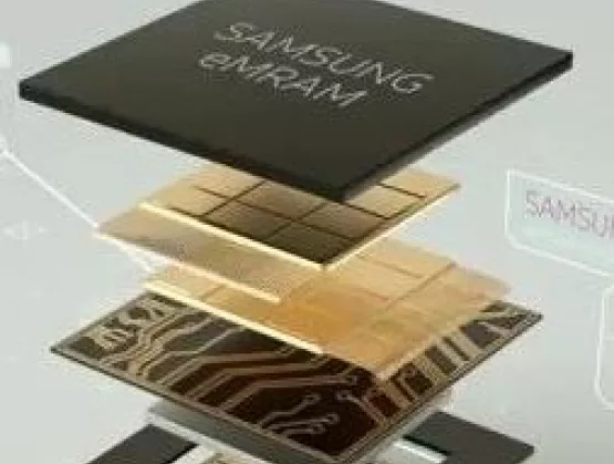
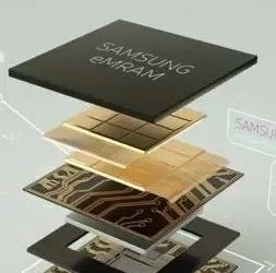
[caption id="attachment_11865" align="alignleft" width="300"] (Courtesy: eVaderis, SOI Consortium)[/caption] eVaderis CEO Jean Pascal Bost talked about how data-intensive IoT applications are enabled with FD-SOI and embedded magnetoresistive non-volatile memory (eMRAM) technology. You can get the slides from his talk here. eVaderis has eflash-like and eSRAM-like eMRAM IP that covers most MCU applications. They also have an eMRAM compiler tool and high-value-added IP for 22FDX. They foresee impressive power savings at the system level with body biasing: 25x this year and up to 45x in 2020, so that intelligence can be brought to IoT. In February they announced that they are co-developing an ultra-low power MCU reference design using GF’s eMRAM technology on the 22FDX® platform. And in March eVaderis and Mentor/Siemens announced that eVaderis proprietary Magnetic Tunnel Junction (MTJ) model would be co-optimized with AFS to speed-up simulations and generations of embedded MRAM IPs and compiler products with good accuracy.An 22FDX MCU reference design project is underway, with tape-out in July '18. Reduced Energy Microsystems (REM) CEO William Coven talked about realizing near-threshold computing with 22FDX and low-power memories. REM has two products on 22FDX: their Neuron Vision SoC and 64-bit RISC-V IP cores. 22FDX, he says, has been fantastic. Simgui Jeffrey Wang, the CEO of wafer-maker Simgui looked at why China is promoting its IC industry. (In the SOI ecosystem, Simgui is particularly known for its RF-SOI wafers, which it produces using Soitec's Smart CutTM process.) This was more of an overview talk, not necessarily specific to the SOI ecosystem, but certainly interesting. In terms of worldwide semiconductor sales, he said, about half end up in China. The CICF – aka the Big Fund – is currently running at about $74 billion. Having realized that mergers acquisitions would not solve the problem, they've opened a second round, targeting another $160 billion. China's two biggest innovation success stories are Huawei (with its Kirin processor), and China Rail, which is now a global Fortune 500 company. The CAGR for the China semiconductor industry is 19%, though they need 20% to reach their goals. IC design is a particularly successful area, posting a CAGR of 29%, with two players in China in the top 10 worldwide. Packaging and assembly/test are also very strong. Zing is working on increasing the supply of 300mm silicon wafers, while Simgui is expanding in both 200 and 300mm capex, due to “big demand”, he said. Panel Discussion [caption id="attachment_11866" align="alignleft" width="300"] SOI Symposium Panel Discussion: (left to right): Giorgio Cesana (Co-Director SOI Consortium), Dave Eggleston (VP GF), Tim Saxe (CTO, Quicklogic), Wayne Dai (CEO, Verisilicon), Samir Patel, (CEO Sankalp Semi), Kelvin Low (VP, ARM), Mahesh Tirupattur (EVP, Analog Bits)[/caption] The day wrapped up with an excellent panel discussion moderated by SOI Consortium Executive Co-Director Giorgio Cesana. Here are a few of the observations made by the panelists. QuickLogic CTO Tim Saxe said that FD-SOI made their designs more compact. With FD-SOI for FPGAs, you've got one set of IP, and you can decide at runtime where you're going for low power or high performance. With a lot of power domains, you see the benefits at the system level. GF VP Dave Eggleston said they're seeing early adopters of eMRAM, especially for wearables with RF and low power. ARM VP Kelvin Low said people should do more than just migrate to FD-SOI. If they use back biasing, it can replace the need for big/little cores. Body biasing makes things easier, maintained Verisilicon CEO Wayne Dai. His teams find that with body biasing, you can tape out for “typical” instead of “worst case”. It's not too late for FD-SOI: it's perfect timing for the MCU market, which is still at 40nm, said Sankalp Semi CEO Samir Patel. As designers, they're happy to focus on companies still on the older nodes. The IP ecosystem should be more enthusiastic about FD-SOI, said Analog Bits EVP Mahesh Tirupattur. You've got more potential customers, and your volume runs can be bigger. In his closing remarks, SOI Consortium Executive Co-Director Carlos Mazure reminded the audience of the day's three take-aways: power consumption is driving even systems companies FD-SOI is penetrating fields like MCUs and SoCs where more intelligence is needed China is still a really big opportunity.
Read More