downloadGroupGroupnoun_press release_995423_000000 copyGroupnoun_Feed_96767_000000Group 19noun_pictures_1817522_000000Member company iconResource item iconStore item iconGroup 19Group 19noun_Photo_2085192_000000 Copynoun_presentation_2096081_000000Group 19Group Copy 7noun_webinar_692730_000000Path
Skip to main content
Default Banner Image

Administrator

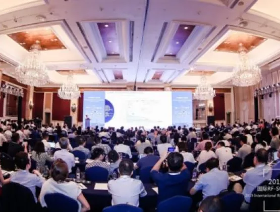
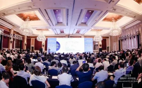
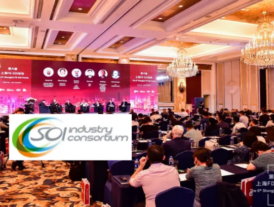
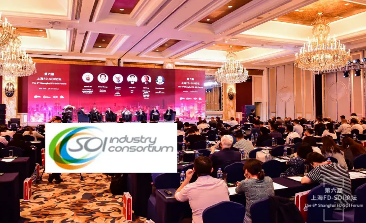
The recent SOI Consortium’s FD-SOI and RF-SOI events (Shanghai, September 2019) were record-breakers, with attendance approaching 1000 over the two days. The event was extensively covered in the China tech press, which often cited the opportunities SOI-based technologies offer for technology leadership. Indeed, as SOI Consortium Executive Co-Director Carlos Mazure noted in a follow-up press conference, the SOI technology drivers dovetail perfectly with the semiconductor industry’s top growth drivers*: IoT, 5G/smartphones, AI/ML and automotive. Here are the takeaways he cited from the China events:SOI for AIoT, consumer and automotive: the FD-SOI ecosystem is in place (substrate supply, foundry offering, EDA and design IP). The 1st wave of adoption is ramping at NXP, STMicroelectronics, Sony, Rockchip, Synaptics, Renesas and more Fast followers are lining up, with the number of tape-outs increasing at Samsung and GlobalFoundries SOI for 5G: development is driven by the need for low cost, low latency and high data throughput the SOI ecosystem for 4G/5G technologies is in place with a strong market pull RF-SOI, the reference FEM 4G technology, will extend its benefits to sub-6Ghz: low power consumption, high linearity, low insertion loss, co-integration of RF components. 5G mmWave requirements are addressed by multiple SOI platforms (RF-SOI, PD-SOI and FD-SOI) enabling integrated analog mixed signal solutions at low power consumption. Two RF-SOI luminaries were honored at a post-event dinner sponsored by China wafer purveyor, Simgui. Jim Cable, Chairman and CTO of pSemi, a Murata Company, and Herb Huang, CEO and GM of Ninbo Semiconductor received awards for their contributions to the advancement of RF-SOI (more on this later). There’s an enormous amount to tell you about from the conferences, so this will be the first round-up post of several.Gitae Jeong, SVP, Samsung Electronics (Courtesy: VeriSilicon live.photoplus.cn) But briefly, in his talk entitled, "IoT Platform with FDSOI", the main points made by Gitae Jeong, SVP, Samsung Electronics were: 28FDS is fully mature. It has the same design rules as bulk, has an integrated security key, a wide range of packaging options for IoT, and a design guide that makes back biasing easier and simpler with complete IP solutions. 18FDS development is on track for this year, with 14nm BEOL and a 35% increase in performance, a 55% decrease in power (!) and a 35% decrease in area compared to 28nm. 1st products are now shipping with eMRAM on 28FDS with yields over 90%, operating temperatures have been extended to 125C for automotive, and a 1Gb version has been demo’d. 1st 5G products mmWave products on 28FDS are now available Americo Lemos, SVP, GlobalFoundries (Courtesy: VeriSilicon live.photoplus.cn)In his talk, "Leading Industry Innovation by Differentiated SOI-based Solutions", key takeaways made by Americo Lemos, SVP, GlobalFoundries included:They have leadership in RF-SOI, with over 50 billion chips shipped 22FDX (FD-SOI) is in production. Last year they had 14 tape-outs, this year they had 26 – half of which are for companies in China. By the end of this year they’ll have shipped 100 million good dies to customers, marking the full transition from ramp to volume. In the ecosystem, they’ve got 285 IP titles from providers worldwide, with more announcements coming soon. Work continues on 12FDX – more to come on this. Edge AI is the next growth engine for IoT, combining vision + voice + audio, with China coming in strongly with ultra-low-power design for home connectivity, industrial, personal and medical applications. The RF-SOI day was lead off by the reading a letter from Dr. Xi Wang. The leading proponent of SOI in China for over a decade as head of the Shanghai Academy of Sciences, he’s now the country’s Vice-Minister of Science Technology. Until this year, he’s always had the first keynote at the SOI Consortium events in China, but this time he was in a meeting with the VP of Russia. However, his warm letter confirmed his support for the SOI ecosystem, especially the role of SOI-based technologies for China in the 5G era. Danni Song, China Mobile Project Leader. (Courtesy: Simgui live.photoplus.cn) This was followed by a talk by the ever popular and insightful Project Leader Danni Song of China Mobile, the largest of the operators there. China issued 5G licenses in May 2019 as the country gears up for 5G commerce. By next year, 5G will be deployed in all cities above the prefecture level. For now, it’s all about sub-6GHz. The challenge, she noted, is in power consumption, which is 2-3x that of 4G in base stations and devices. They see two development spaces: one for consumer and one for verticals, and have teamed up with Sprint on a 5GS (S being for Superior) module. They released a basic modem chip and dongle in June, and a smart chip is coming. She suggests people consult the China Mobile white paper on 5GS for more info. We’ll cover the many other presentations over the next few weeks – so stay tuned! --------*as cited in a 2019 CEO survey by KPMG/GSA.
Read More
Since the beginning of the year, there’s been a steady stream of excellent news around Samsung Foundry’s 28FDS, their highly successful 28nm FD-SOI offering. Let’s take a look at what’s been happening, as things do seem to be accelerating. By way of reminder, they announced the industry’s first eMRAM (embedded MagnetoResistive RAM) testchip tape-out milestone on 28FDS in September 2017 (you can read the press release here) - which was just a year after they had announced mass production of 28FDS process technology.At the end of 2018, Arm announced the industry’s first Embedded MRAM (eMRAM) compiler IP built on Samsung Foundry’s 28FDS process technology. Follow that with this announcement at the beginning of 2019: Soitec Expands Collaboration with Samsung Foundry on FD-SOI Wafer Supply. The two companies announced that Samsung had secured a high-volume supply of FD-SOI technology to meet industry's current and future demands especially in consumer, IoT and automotive applications. In March came two more big announcements. First: Samsung Electronics Starts Commercial Shipment of eMRAM Product Based on 28nm FD-SOI Process. As they noted in the PR, “Samsung’s 28FDS-based eMRAM solution offers unprecedented power and speed advantages with lower cost. Since eMRAM does not require an erase cycle before writing data, its writing speed is approximately a thousand times faster than eFlash. Also, eMRAM uses lower voltages than eFlash, and does not consume electric power when in power-off mode, resulting in great power efficiency.”Hard on the heals of that came the news that Arm and Samsung Announce IP Platform including eMRAM for 18nm FD-SOI. At the SOI Consortium’s Silicon Valley Symposium in April, Tim Dry (he’s Samsung’s Director of Foundry Marketing for Edge and End Point), gave a terrific presentation. Entitled Samsung’s FDS with MRAM: Enabling Today’s Innovative Low Power Endpoint Products, it details the company’s FDSOI roadmap for the IoT Endpoint Platform (and yes, you can download in its entirety). Then in May at the big Samsung Foundry Forum in Silicon Valley, Arm, in collaboration with Samsung Foundry, Cadence, and Sondrel, demonstrated the first 28nm FD-SOI eMRAM IoT test chip and development board. The Musca-S1 test chip demonstrates a new choice in SoC design for IoT solutions, said Arm. (Sondrel, btw, is Europe's largest independent IC design consultancy.)In parallel, Cadence announced: Cadence Custom/AMS Flow Certified for Samsung 28nm FD-SOI Process Technology. Especially aimed at digitally-assisted analog designs, what’s new here is that the Cadence custom and analog/mixed-signal IC design flow is now Samsung Foundry certified for 28FDS. Samsung’s 28FDS PDK techfile is Mixed-Signal OpenAccess ready, enabling customers to deploy OpenAccess-integrated, fully interoperable Virtuoso-Innovus implementation flows. For its part, at its Foundry Forum, Samsung unveiled extensions of the company’s FD-SOI (FDS) process and eMRAM together with an expanded set of state-of-the-art package solutions. They indicated that the development of the successor to the 28FDS process, 18FDS, and eMRAM with 1Gb capacity will be finished this year.And finally, companies like NXP are shipping exciting new products fabbed on Samsung’s 28FDS. Ron Martino, VP GM of NXP’s i.MX Application Processor Product Line covered key products in his presentation at the SOI Consortium’s Silicon Valley Symposium (see our coverage here). Among them: the i.MX7ULP for long battery life with 2D 3D graphics for wearables and portables in consumer and industrial applications; the i.MX 8 and 8X subsystems for automotive and industrial applications; and the i.MX RT series of “cross-over” processors. The i.MX RT ULP (real-time, ultra-low-power) series, which Martino says is the “new normal”, deals with a high number of sensor inputs. The i.MX RT 1100 MCUs, which have been qualified for automotive and industrial applications, are breaking the gigahertz performance barrier.In July, linuxgizmos.com reported that, “In June, NXP began volume shipments of its super power-efficient i.MX7 ULP, which it announced in 2017. The SoC is billed as the most power-efficient processor on the market that also includes a 3D GPU. […] the ULP version includes a 3D graphics capable Vivante GC7000.” (Vivante, btw, is a VeriSilicon company, which is an SOI Consortium member and a leading proponent of FD-SOI design and IP in China and worldwide.) This is leading to some really nice wins for NXP. For example, they’ve got Amazon's Alexa Voice Service (AVS) leveraging the i.MX RT crossover processor, enabling developers to quickly and easily add Alexa voice assistant capabilities to their products. The RT series has rapidly been expanded, with versions for voice-controlled devices and offline face and expression recognition capabilities for smart home, commercial and industrial devices.Also announced this summer: NXP and Microsoft Bring Microsoft Azure Sphere Security to the Intelligent Edge with a New Energy-Efficient Processor. That collaboration includes development of a new crossover applications processor in NXP’s i.MX 8 series integrating Microsoft’s Azure Sphere security architecture and Pluton Security Subsystem. Their customers “will be able to harness the high-performance and energy efficiency of NXP’s i.MX 8 applications processors combined with Microsoft’s unequaled security and assurance provided by Azure Sphere certified chips”. As Martino concluded in his presentation, “The future of embedded processing [is] enabled by FD-SOI.” And Samsung Foundry’s FD-SOI offerings are clearly a massive enabler of that future.
Read More
ASN had a chance to talk to François Brunier of Soitec, who’s leading this important project.Advanced Substrate News (ASN): Can you tell us briefly about OCEAN12?Francois Brunier (FB): OCEAN12 stands for Opportunity to Carry European Autonomous driviNg further with FD-SOI technology up to the 12nm node.Francois Brunier, Partnership Program Manager, Soitec.OCEAN12 deals with “Ultra-low power computing solutions for automotive and aeronautics using all the range of FDSOI technologies”. This project with a budget of 103M€ brings together 27 partners from 7 different countries. The project received the ECSEL JU* label under the 2017 call. ECSEL is an EU-driven public-private partnership enabling the co-financing of innovation in electronic components and systems both by Member States and the European Union.ASN: Why is this project needed?FB: As of today a car has around 500 million transistors. These electronic components represent already an important vector of valorization and differentiation for the automotive industry and for the consumer. The increased autonomy of the vehicles will require a very strong build-up of computational capacities. 50 to 100 times more transistors could be required for a level 5 (fully autonomous car). Following this trend an autonomous car will require power consumption equivalent to 50 to 100 computers running continuously (without taking into account the car propulsion).The OCEAN12 partners.The power consumption of these components becomes a key element in the choice of technologies. We believe that our technologies on SOI present the best assets to meet this challenge.The FD-SOI substrates, technologies and designs developed in OCEAN12 offer a palate of different solutions to this challenge: increased performance for data processing (including Artificial Intelligence); much higher energetic efficiency; and smaller form factors to fit in embedded systems like autonomous cars with higher integration and reliability, and enabling safe connectivity.The OCEAN12 project will demonstrate that SOI technologies are able to meet these challenges through relevant demonstrators in the targeted fields.ASN: What are the project goals?FB: OCEAN12 will bring concrete solutions to the main challenges of smart connectivity and low power consumption in the automotive industry.As such, OCEAN12 will build awareness around the key enabling technologies in substrate development, transistor behavior, and the design and fabrication of integrated circuits up to the system and end-user application levels. We will show that the technology is advantageous for automotive and aerospace applications, which are strategic sectors for Europe. Having the whole supply chain in Europe means having trusted and secured components made in Europe.The OCEAN12 project goals stand on three pillars:First: Confirming the technology foundation. Ocean12 puts the FD-SOI substrate and device developers in direct contact with the full value chain of suppliers and end users. This gives the entire ecosystem visibility into current and future needs, and ensures that substrate and device solutions are both technically feasible and correctly aligned with actual system requirements.Second: Creating concrete, innovative demonstrators in automotive (Audi, Bosch) and aeronautics (Airbus, Thales). These demonstrators are a first step in defining the context and environment to prove the advantages of these technologies in real application cases, showing they are useful and as such prefigure a final system and a potential future product roadmap. Demonstrators should be as close as possible to the final application.Third: Broadening the design ecosystem, with the big companies, the small- and medium-sized companies (SMEs) and the research organizations (universities, RTOs). We have a critical mass of 16 design ecosystem partners focusing their efforts on FD-SOI. The project leverages that dynamic FD-SOI design ecosystem for IC product migration to FD-SOI and the creation of new IP. Inventing the future components in Europe is also key.ASN: Can you tell us more about the demonstrators? When will we see them?FB: There are four demonstrators. All these demonstrators will be delivered by the end of the project in 2021:Always-on wake-up systems (Audi, Bosch, Leti). With such a system we can imagine an application to monitor our car when it is parked in a parking lot for a long time. The sensors would remain aware of everything that goes on around the car. Based on sensor observations, the car can make decisions on further actions to take. This can be used in many future car applications like intrusion detection or vehicle access systems. But you will not have to worry about battery drain: even though all the sensors are always on, they go right back into a very low-power sleep mode thanks to FD-SOI technology.mm-Wave integrated radar SOCs (Bosch and Audi), which will benefit from all the innovations of FD-SOI thanks to its low consumption properties, but also the optimization of the sensors. The performance gain is made over the entire system with adaptations between analog and logic.High-performance video processor for aeronautics. (Airbus, Thales, Kalray). Kalray, a French SME working on Massively Parallel Processor Arrays (MPPA) aims to demonstrate an ultra-low power, low-cost, high-performance neural processor on FD-SOI technology. This demonstrator would be key for Airbus and drones with high-performance, low-power cameras. Airbus and Audi have partnered on air and ground mobility services.Microcontroller plug-and-play board. This demonstrator lead by ST will allow for the development of new solutions in the domain of GNSS/GPS.ASN: Can you tell us more about the partners?FB: The OCEAN12 consortium of 27 partners involves 8 large groups, 9 SMEs and 10 universities/RTOs. These partners come from 7 different European countries.The eight large groups include: Soitec, the world’s leading provider of FD-SOI substrates; EVG, a leading global equipment supplier; GlobalFoundries and STMicroelectronics, the two major European FD-SOI foundries; and Bosch, as a Tier 1 automotive supplier. At the top of the value chain, high-end European automotive manufacturer Audi, the avionics industrial giant Airbus, and Thales for security issues, will develop product demonstrations.Ten highest-level research institutes support the industrial consortium. They include CEA-Leti (FR), Fraunhofer(GE), IMS (FR), INP Grenoble (FR), TU Dresden (GE), U. Paderborn (GE), Bundeswehr U. Munich (GE), Eberhard Karls U. Tübingen (GE), Instituto de Telecomunicações (PT), and Warsaw UT (PL). They increase the competitiveness through technological innovation and transfer of technical know-how while gaining new expertise working with global leaders.In addition, OCEAN 12 has a very strong SME consortium covering the supply chain in the fields of new equipment, IP, system integration and fabless companies. They include: IBS, UnitySC (HSEB), MunEDA, Kalray, AED Engineering, ISD, EVOTEL, M3 Systems and Design Reuse.All these partners have longstanding experience of cooperation in various national and international frameworks and are specialists in their fields of activity. Their contributions are essential for the success of the project.ASN: What is the timetable?The OCEAN12 kick-off event at Soitec’s headquarters near Grenoble.FB: The project started on April 1st 2018. The kick off with all the partners was held at Soitec on 29 September 2018. It was a great success. The project runs through December 2021, by which point everything has to be demonstrated.ASN: Can you clarify the funding structure?FB: The budget is about €103.6M. If the project succeeds, we get European Commission funding. In that case, just over 20% of the eligible cost – about €23M – is subsidized at the European level. The seven countries with companies or organizations participating in the project will then roughly match the European subsidies, contributing about €27M. These ECSEL-type public-private projects are a tried and true model in Europe, maximizing synergy across ecosystems. To conclude, in the name of the consortium I’d like to thank the ECSEL JU, the European Commission and our National Funding Agencies from France (DGE), Germany, Portugal, Greece, Spain, Austria and Poland. Such a project would not exist without them.______*ECSEL JU: Electronic Components and Systems for European Leadership Joint Undertaking
Read More
Renesas, one of the world’s very top MCU manufacturers, is heralding its new FD-SOI based R7F0E017 for energy harvesting applications. In an in-depth article in the May 2019 edition of EENews Embedded, Renesas Product Marketing Manager Graeme Clark detailed the new chip, which is sampling this year. It’s a fascinating read, with lots of explanations about how SOI enables the cutting-edge features (like an integrated energy harvesting controller) – you won’t want to miss it. BTW, here at ASN we’ve been covering the origins of this technology since 2005.They call it SOTB, for Silicon On Thin Box, but it is indeed their flavor of FD-SOI. The work started at Hitachi in cooperation with Renesas with a paper that debuted at IEDM 2004, then moved along through the series of mergers that resulted in the offering at what is Renesas Electronics today. Here are some key quotes from the article:“The new SOTB process can now offer active mode current of less than 20 µA/MHz and leakage currents down to 150 nA, while still allowing the development of devices with reasonably high clock rates, large embedded flash memories and SRAMs on chip. This combination of integration and power consumption will make devices developed on this process ideal for energy harvesting applications. The result of this new process is that we can develop a new generation of microcontroller products.” “The use of the Silicon on Thin Buried Oxide technology on this new device has resulted in some unique low power characteristics. The first device has the following features and future devices using this process could offer even lower power consumption. Active current of 20 µA /MHz Standby Current of 200 nAADC operation 3 µA @ 32 kHz256 Kbyte SRAM with 1 nA / Kbyte standby current” “The R7F0E017 is able to run safely from a pure energy harvesting power source due to the operation of the Energy Harvesting Controller. The device can operate from a wide range of potential energy sources including solar power, vibration, pressure and temperature difference, and many others. The integrated energy harvesting controller, supported by very few inexpensive external components, completely manages the cyclic wake-up sequence of the microcontroller, only using the extremely low energy harvesting source current.”Click here to read the full article on the eenewseurope website.
Read More
2019 will be a busy fall for the SOI Consortium and our members.First off are the SOI Consortium events in Shanghai and Tokyo, which are very popular indeed. We now have the dates locations locked in, so you’ll want to mark your calendars:Shanghai: 16 17 September 2019, FD-SOI Forum / RF-SOI Workshop. Both days will be held at the Pudong Shangri-La Hotel in Shanghai. The first day will focus on FD-SOI. The second day is all about 5G and RF-SOI. These are huge events – to get an idea of the magnitude, you can read our coverage of the 2018 event. Tokyo: 30 31 October 2019, Japan SOI Design Workshops. This year both days of workshops will take place in the Yokohama Landmark tower. The first day will be devoted to FD-SOI; the second day turns to More-Than-Moore – especially photonics and MEMS. Last year’s workshops were packed with excellent presentations and panel discussions, which we covered here. The SOI Consortium and members will also be giving talks at Semicon Europa, which is being held 13 – 15 November 2019 in Munich, Germany. The programs are currently being finalized. As soon as they’re ready, we’ll be sure to let you know so you can register and/or share the news with your colleagues and clients. But in the meantime, make sure you save the dates.Would you like to check out the presentations given at Consortium events in previous years? If you hover your cursor over the Events tab at the top of our home page, you’ll get a drop-down menu of events for the last five years (we’re working on adding more – we’ve been doing these events for over a decade!). Click through to any past event and you’ll land on a page where you can download most of the presentations that were given there. Of if you’re looking for past presentations given by any particular company, use the search engine at the bottom of any page on our website. S3SYou’ll also find many of our members at the IEEE/EDS S3S Conference in San Jose, CA, October 14 – 19th. S3S (formerly known as The SOI Conference) has been running in various forms for over 30 years. They always have an excellent line-up of speakers, plus it’s a great opportunity for networking with researchers from across the worldwide SOI ecosystem. BTW, while the deadline for general paper selection has already closed, papers of exceptional merit are currently being accepted for their Late News Sessions. See the 2019 Call for Papers for more information – those Late News papers need to be received by 23 August 2019 for consideration. Also, IEEE S3S Conference will once again host a full-day short course and a half day tutorial. These are very popular. The short course this year will be on SOI Design and Technology for Analog and Mixed Signal. As of this writing, the program is still being finalized, but more will be announced in the next few weeks, so check back on their website soon for updated information.Member EventsAnd finally, don’t forget to learn more about the offerings from and in support of the SOI ecosystem at our members’ events around the globe, including: GlobalFoundries – GTC | Samsung Foundry – SFF | ST – Technology Tour | Synopsys – SNUG | Cadence – CDNLive | Silvaco – SURGE | Arm – TechCon | NXP – Tech Days | Leti – Events | imec -Events |
Read More
If you’re going to Semicon West this year, be sure to attend the SOI Consortium’s workshop on how IoT is driving the SOI supply chain. There’s a great line-up of speakers – see the program below. IoT means many things to many people but everyone agrees it’s here and growing quickly. IoT, including machine learning and movement to the edge, is fueling innovation as the high compute and ultra-low energy requirements are pushing technology to deliver on these needs. The well-known characteristics defining IoT of “Sense”, “Compute”, and “Act” put additional burden on technology to full these requirements across a variety of use cases and environments without sacrificing reliability or quality. All the various forms of SOI technology from FD-SOI to High-Voltage to RF-SOI, are uniquely situated to deliver on the promise of today’s as well as tomorrow’s IoT roadmap. The supply chain for all forms of SOI technology is in place. This workshop will discuss the current and future solutions from a supply chain perspective.Speakers include experts from SOI Consortium members Applied Materials, NXP, GlobalFoundries and Soitec.Entitled The Internet of Things, Driver of the SOI Supply Chain, the workshop will take place at the Moscone Center South, Wednesday July 10th in Room 301. It will run from 1 pm until 4:30 pm. Anyone and everyone who is registered for Semicon West is welcome. Here is the sign-up page.It’s a great program: 1:00pm - Welcome by Semi1:10pm - IoT/AI/Edge Market – Using SOI Through-out, Jon Cheek, Senior Director, NXP1:35pm - The SOI Opportunity, Manish Hemkar, Director, Semiconductor Products Group, Applied Materials2:00pm - The Foundry IP Ecosystem, Jamie Schaeffer, Sr. Director, GlobalFoundries2:25pm - Engineered Substrates - Enabling the IoT Revolutions, Eunseok Park, Director, Emerging Technology in Strategic Marketing, Soitec 2:50pm - Enabling the SOI Era, Thomas Uhrmann, Head of Business Development, EVG3:15pm - Panel: The Internet of Things, Driver of the SOI Supply Chain, Moderator: Carlos Mazure, Chairman, SOI Industry Consortium. Panelists include:Manish Hemkar, Director, AMATYoshio Kitahara, President Managing Director, Kokusai EuropeThomas Uhrmann, Head of Business Development, EVGJon Cheek, Sr. Director, NXPThomas Piliszczuk, EVP Strategy, SoitecJon Kretzschmar, Manager of Product Sales Marketing, TEL America4:05pm - Closing remarks, Carlos Mazure, Chairman, SOI Industry Consortium4:20pm - EndThis is a great chance to learn more about SOI and the SOI Consortium. Don’t miss it!And while you’re at West, you should also check out a related event. SOI Consortium member Leti will be teaming up with Fraunhofer for a workshop entitled New Paradigms in Microelectronics–Providing R D for the 21st Century. That happens at the nearby W Hotel in San Francisco on Tuesday, July 9th at 5:00pm. Click here for more information on that.
Read More
The SOI Consortium and member companies had a significant presence at two important events in China recently: the World Semiconductor Congress (WCS) in Nanjing and the SOI Academy, including an FD-SOI Training Day in Shanghai. Nanjing is especially known as a leading RF chip design hub in China, but WCS went well beyond RF. The three-day 2019 event was held at the Nanjing International Expo Center. It attracted over 30,000 visitors, 5000 of whom attended the various summit forums. Presenting at WCS '19 in Nanjing (clockwise from top left): Wayne Dai, CEO/Founder, VeriSilicon; Carlos Mazure, Executive Director, SOI Consortium; Giorgio Cesana, Director, STMicroelectronics; Christophe Tretz, Design Expert, SOI Consortium. (Photos courtesy: WCS)The SOI Consortium organized the SOI Forum, which was part of an afternoon Innovation Summit. Presentations were given by members of the SOI Consortium team, and by leaders from our membership, including Simgui, NXP, Incize, ST, IBM, Cadence and Xpeedic. Some of those presentations are now available from our website -- click here to get them.Earlier in the day, SOI Consortium member VeriSilicon participated in a morning session on AI and IoT Wireless Communications. They presented their low-power Bluetooth design platform for GlobalFoundries 22FDX, and CEO Wayne Dai moderated a lively round-table discussion.Following hard on the heels of the Nanjing event, the SOI Consortium team and members headed to Shanghai for the SOI Academy 2019, hosted for the second year in a row by member SIMIT (Shanghai Institute of Microsystem and IT under the Chinese Academy of Sciences). The two-day event attracted more than 250 professionals from more than 100 domestic and foreign IC companies and research institutes. Keynotes by SOI Consortium Executive Director Carlos Mazure, SITRI CEO Mark Ding and Jean-Eric Michallet, Head of the Microelectronics Components Department at Leti and bizdev director for the SOI Consortium focused on the SOI ecosystem. The SITRI and Leti talks also gave updates on their research and industrialization alliance. Further talks were given by leaders from Soitec, GlobalFoundries, VeriSilicon, IBM and Xpeedic. These addressed the growing FD-SOI ecosystem, applications in automotive electronics, 22 nm and 10 nm FD-SOI devices, advanced SOI substrate technology, China’s FD-SOI development, the FD-SOI manufacturing process, product design, EDA tools and all aspects of industry’s software and modeling value chain.Several speakers noted that more and more local Chinese customers are actively adopting FD-SOI for low-power, high-performance chips. SOI Academy, Shanghai, 2019, FD-SOI Training Day attendees.(Photo credit: SIMIT)The second day was devoted to hands-on professional training, given by experts from Leti using an actual PDK and punctuated by in-depth discussions. This helped the IC designers to fully understand the advantages and flexibility of FD-SOI in low-power logic, analog/mixed-signal and RF. All in all, “It was a great success,” concluded Jean-Eric MICHALLET, Head of the Microelectronics Components Department at Leti and bizdev director for the SOI Consortium. Plans for the next SOI Academy are already underway, with plans to extend the topics to include more on photonics, RF, power and MEMS.
Read More