downloadGroupGroupnoun_press release_995423_000000 copyGroupnoun_Feed_96767_000000Group 19noun_pictures_1817522_000000Member company iconResource item iconStore item iconGroup 19Group 19noun_Photo_2085192_000000 Copynoun_presentation_2096081_000000Group 19Group Copy 7noun_webinar_692730_000000Path
Skip to main content
Default Banner Image

SEMICON Europa

Ischemic stroke is the leading cause of long-term disability worldwide, affecting over 13 million people each year and costing tens of billions of dollars. Sensome, a French medtech that offers connected medical devices, has developed micrometric AI-powered impedance sensors that can identify the biological nature of the tissue they touch in real-time. Integration of this proprietary technology into a probe to guide medical devices in arteries (a guidewire) has given rise to Sensome’s first product, Clotild®, which recognizes blood clot types in ischemic strokes so clots can be treated faster to improve patients’ chances of a full recovery. The Sensome technology also helps transform the current standard of care in oncology.SEMI spoke with Franz Bozsak, CEO and co-founder of Sensome, about innovative medical technology trends and how microelectronics plays a crucial role.SEMI: When did your adventure with Sensome start? Bozsak: My former Ph.D. advisor Abdul Barakat and I spun-out Sensome from the Ecole Polytechnique in Paris in early 2014 after receiving a 200.000 Euro grant from the French government. We then developed a micrometric impedance sensor that coupled to machine-learning algorithms to identify biological tissues on contact. We are still integrating this sensing technology with existing medical devices in order to create a new category of smart medical devices that provides physicians with relevant insights during their interventions and treatments. These additional insights aim to render healthcare treatments more effective by reducing the risk of complications and the cost of interventions while improving patient monitoring.SEMI: How are strokes typically treated? Bozsak: Before 2014 the almost exclusive way of treating ischemic stroke was by injecting tissue plasminogen activator (tPA) intravenously in order to chemically dissolve an arterial clot. This treatment approach has severe limitations and can only be used in the first 4.5 hours following the onset of a stroke. In 2015, several randomized clinical trials demonstrated the efficacy of a new treatment modality: mechanical thrombectomy.Medical devices that allow a clot to be removed mechanically either using a grid-like structure (a stentriever) or by aspirating the clot using an aspiration catheter completely changed the paradigm in the treatment of ischemic stroke for up to a third of all patients. This new intervention removes the clot in up to 90% of all cases and can for certain patients be used up to 24 hours after the onset of the stroke.Mechanical thrombectomy is now one of the most effective medical treatments in the world. The clinical data gathered over the past years also shows that, in order to maximize the patient’s chances to lead a life free from disability after a stroke, it is not only a question of getting the clot out but also about how the clot was removed. Removing the clot on the first attempt significantly increases the patient’s chances of recovery – the first-pass-effect that is now the objective when treating ischemic stroke patients. And this is exactly where Sensome wants to help since clot removal after several attempts increases risk for patients. SEMI: How did you improve mechanical stroke treatments?We have integrated our sensor technology into a guidewire, the first device to enter a patient’s blood vessels for navigation to the clot. Once in place, the smart guidewire – called Clotild® – guides the thrombectomy device to provide the physician with information on the clot to help the physician choose the thrombectomy device with the highest chances of achieving the first-pass-effect. SEMI: Medical technology has made astonishing advances over the years. How did Sensome develop the micrometric AI-powered impedance sensors?Bozsak: The development of a product like Clotild® would have not been possible five years ago, and many people considered what we wanted to achieve simply incredible. Today, we can answer those same people: We knew it was almost impossible and therefore we just did it. By combining diverse semiconductor technologies, we were able to build the smallest impedance meter in the world. This was then integrated into a guidewire that can be connected via a transmitter to a tablet that serves as the interface with the physician. The guidewire provides impedance measurements that can be analyzed by a machine-learning algorithm, which in turn identifies the tissue in contact with the sensor. A very diverse team of people, collaboration and several different disciplines such as micro-electronics, data science, biology and engineering were required to make this happen.Our ambitious team has been able to flourish and accomplish their ideas in the very stimulating and resourceful environment of the Ecole Polytechnique, while being embedded into the rich and fertile start-up ecosystem of Paris. It is the combination of all these factors taken together that have made our innovation possible.SEMI: What are the main challenges and what are the market opportunities? Bozsak: Bringing semiconductor technology into the medical field is not a straightforward process. The primary hurdle is the simple fact that medical device production volumes are not comparable with consumer electronics volumes and that development cycles are much longer due to regulatory constraints. Both factors are, at first sight, not necessarily compatible with today’s business model of the semiconductor industry. At the same time, this is also a unique opportunity for the semiconductor industry to diversify and expand into a new field – sensors and, in particular, their seamless integration into the healthcare workflow, are a key driver for the healthcare sector of the future. And to achieve this objective, semiconductor technologies are key. What is beneficial, in my opinion, is that the quality standards and requirements of the semiconductor industry are highly compatible with the needs of the medical device industry.SEMI: Are market fragmentation and the high level of regulation making medtech innovation harder?Bozsak: Both are challenging but very rewarding to pursue since the impact on a patient’s life can be profound. Innovation is harder because many stakeholders are involved in ensuring the success of a medical device launch. The involved, milestone-driven, highly regulated process of developing a medical device and bringing the device to the market assures its eventual success. The development process differs very much from those for normal consumer devices. In our case the beneficiary, the patient, is not necessarily the user of the device but rather the physician. The physician is not necessarily the buyer of the device, but the hospital. The hospital is not necessarily paying the device, but ideally the government.The interests of all these stakeholders need to be satisfied to bring a successful device to the market.SEMI: What are your expectations regarding the future of medtech digital innovation? Bozsak: This is the right moment for the medical device and semiconductor industries to come together. The healthcare sector is not low on medical needs for which innovative ideas exist, and the semiconductor industry has many technologies that can enable these ideas to generate solutions. But to make this happen, both sectors need to collaborate. Working together requires both sides to understand their respective needs and constraints. The earlier the knowledge exchange starts, the more powerful the solutions. SEMI MedTech Forum at SEMICON Europa last year was a wonderful opportunity for Sensome to get this discussion going. We are looking forward to continuing the exchange and push the frontiers of the possible further to create the future of digital healthcare.Franz Bozsak, CEO and co-founder at Sensome, obtained a M.S. in Aerospace Engineering from the University of Stuttgart and a Ph.D. from the Ecole Polytechnique in Biomedical Engineering on the optimization of stents. He is a graduate of the Stanford Ignite/Polytechnique business program. In 2014, he co-founded Sensome and has since built a team of renowned scientists, engineers and doctors to realize his vision of connected medical devices. He was named Innovator Under 35 by the MIT Technology Review in 2016. Serena Brischetto is a marketing and communications manager at SEMI Europe.
Read More
Sapphire is a precious gemstone, consisting of aluminum oxide (α-Al2O3) with occasional traces of other elements such as iron, titanium, chromium, vanadium or magnesium. While sapphire stones found in nature mostly go to jewelry applications, the lab-grown sapphire – produced in a scale of up to several hundred tons per year – is widely used by the electronic industry. Now one can hardly find a branch of technology where this crystal is not used.Sapphires are mainly applied in infrared optical components, high-durability windows, wristwatch crystals, and the very thin electronic wafers used as the insulating substrates of solid-state electronics. High thermal conductivity, low reactivity, and appropriate unit cell size make sapphire an ideal material for a wide range of such electronic substrates for manufacturing of components such as LEDs and CMOS chips.SEMI spoke with Ivan Orlov, CEO of Scientific Visual, after his presentation at SEMI Strategic Materials Conference at SEMICON Europa, 12-15 November, 2019 in Munich, Germany, to learn more about the future of sapphire.SEMI: Why is sapphire an ideal material for a wide range of electronic substrates? Orlov: Sapphire undoubted advantages are its chemical inertness and ability to withstand high temperature, radiation and mechanical loads. In addition, it exhibits low dielectric loss and very good electrical insulation that makes sapphire a good candidate for substrates for LEDs and laser diodes or wafers for epitaxial growth. However, the most important advantage is that sapphire crystal lattice does very well matching semiconductor materials deposited to its surface, in particular nitrides of group III elements. To plainly benefit from these features, the grown sapphire must have as few macro- and micro-defects as possible, as substrate defects are inherited by semiconductors layers grown on the substrate surface. Hence the importance to detect defects in the raw sapphire material. This is the area where our team at Scientific Visual contributes. SEMI: Flaws are usually identified only after costly wafering and polishing steps, because rough surface of raw crystals prevents detection of the defects. What can be done to prevent defects?Orlov: Today, major players are investing in growing larger crystals without mastering in depth the growth process. Let’s face it, the semiconductor substrate industry, which is primarily based in Asia, is using empirical research methods. The raw sapphire boules are still inspected manually, and this qualitative assessment is exploited in two folds. The first step is to further process the boule. Furnace operators then adjust the growing parameters depending on the results of the manual inspection.Due to the lack of visibility into internal crystal defects, the crystal growth and its downstream processing remain an art rather than a science. The primary reasons are the difficulty to measure, locate and quantify precisely the defects in the full crystal volume. Scientific Visual equipment enables defects in raw boules to be fully quantified and categorized. With such objective measurements and knowing the full set of growth parameters, the Process Engineering (PE) team can, with the assistance of deep learning algorithms, considerably improve the growing process. Our quality control tools give Process Engineering team the “eyes” to see complete defect distribution in raw crystals, enabling it to make minor modifications in the growth process to improve yields, reduce costs and shorten the time to market for products.SEMI: What lead to those advancements and what problems did your team set out to solve? Orlov: Breakthroughs in immersion tomography, machine vision and parallel computing drove advancements in automated quality control technology. Previously crystal inspection accuracy was limited by the acuity of the operator’s eye and subjective bias. Light distortion and the diffusion of crystals made it impossible to accurately identify internal defects.Scientific Visual equipment give operators an undistorted 3D view of all defects in a crystal boule or ingot. However, only deep learning technology can correlate a hundred thousand growth data points to identify a final defect pattern.Defect pattern in non-processed item cored from EFG sapphire plate. Well visible is a typical wavy pattern of surface layers and sandwich structure in the volume. Color code marks sapphire defect density: from deep blue (non-defective material) to deep red (highest defectiveness.) SEMI: What challenges are addressed by your approach? Orlov: Increasing the yield of semiconductor substrates like Sapphire, Gallium Nitride and Silicon Carbide is paramount to reducing the price of wafers while increasing their quality. The upstream growth and downstream wafering processes are not deterministic. So far, most of the producers can only determine the quality during the late stages of the process. This condition creates huge constraints for teams in charge of production and processing. Automated Quality Control (QC) at the early stage of the production chain relieves all the unknowns, ultimately reduce the cost of material.SEMI: And what are the main opportunities?Orlov: There are massive opportunities to increase the yield and to ease the full processing chain from growth to the wafering process. Objective Quality Control (OQC) paves the way to industry-wide standards that categorize crystal quality at each step of growth to enable full certification of the defectiveness of the material and facilitate its trade and exchange.SEMI: What’s one of your predictions for the future of new materials?Orlov: The explosion of e-mobility and electric vehicles and the development of other green technologies will drive rising demand for low-defect sapphire, silicon carbide and gallium nitride substrates thanks to the streamlining of the full processing chain. Manual quality control will soon give way to full automation as quality control in sapphire and other raw crystals production is the only missing link in a fully automated semiconductor production chain. I believe that in five years, automated raw crystal inspection will become standard in the industry. Our mission is to empower every crystal grower to achieve this important milestone.Dr. Ivan Orlov obtained a Ph.D. in Crystallography from the Federal University of Technology in Switzerland EPFL and an MSc in Solid-State Physics in Moscow, Russia. Ivan co-founded Scientific Visual in 2010 to answer the challenge of the synthetic crystals industry struggling with high defect yield. Prior to this he worked in a company specialized in diamond optics. He has more than 10 years of experience in R D with focus on optical materials, industrial crystals and non-destructive quality control technologies. Dr. Orlov was a SEMI Task Force member for sapphire standard development in China and collaborates with ISO committee in Switzerland to establish industry-wide sapphire quality standards.Serena Brischetto is senior marketing and communications manager at SEMI Europe.
Read More
“A hundred years from now, someone’s going to look back and say, ‘Can you believe they waited until you got a disease, and then they did something?’” This observation from Dr. William Hait, the leader of Johnson Johnson’s External Innovation program, crisply sums up the SEMI Smart MedTech Summit, a two-day program at SEMICON Europa 2019, sponsored by GE Research and imecBenjamin Wiegand, PhD of Johnson Johnson, cited the quote in his opening presentation and added another pertinent question: “What if we could predict who was going to get a disease and then preempt it from happening?” Weigand’s conclusion is the first of six key takeaways from the summit.1. Accomplishing this vision could lead to a world without disease. Developing a disease-free world by exploring how the integration of advanced electronics and medical technology (MedTech) can enable new healthcare solutions is the very mission of the SEMI Smart MedTech Initiative. Various experts speaking at the MedTech Summit delved into a range of topics, from pan-European medical initiatives and artificial organs to new sensors and systems and start-ups’ need for funding and partners.2. All of us will have a digital twin (avatar), bringing together all relevant data that can impact our health and well-being.Several speakers illustrated the advantages of a digital human avatar that would start with an individual’s unique physical data and then be continuously updated with new data tracked by body-worn devices and from ongoing research findings. This would enable healthcare providers to extract insights and predict future physical performance or health issues.While, technologically, the avatar can already be constructed, the ability to make real changes to future human behavior is a significant outstanding question. Multiple speakers highlighted the various benefits of digital avatars at the MedTech Summit. 3. The MedTech sector’s need for cybersecurity looms large, as it does in every other digitally-driven, IOT-based framework.Further exploring the human-to-digital interface, Anthony Mathur of Bart’s Heart Center in the UK pointed to the importance of strict laws for safeguarding patient privacy, a cornerstone of healthcare digital policies, and the critical need for cybersecurity. He warned against an all-digital action network, citing the virus attack that shut down the UK’s National Health Service, rendering all patient records inaccessible for more than two weeks.4. MedTech devices, systems and other tools will radically change healthcare in the not-too-distant future.Almost every speaker touched on this point, including Franz Laermer of Bosch in his presentation The Future of Personalized Treatment. Laermer explored devices that will drive more patient-centric healthcare in areas including asthma therapy and molecular diagnostic testing and highlighted innovations in monitoring oncology therapies more effectively, less invasively and more accurately. Other presenters showcased their work in areas including silicon-based microfluidics, next-generation DNA sequencing and synthesis, lab-on-chip and cell arrays. 5. Startups and well-established companies will help advance digital tools and data to keep us healthier, happier and safer. Among the MedTech Summit highlights, several start-ups presented their business, financial and go-to-market plans. Notably, continuous glucose monitoring (CGM) is an especially active area of investment and innovation, as diabetes is among the world’s most widespread chronic diseases. The industry’s goal is to develop a non-invasive platform as a replacement for today’s prick-and-test approach to measuring blood sugar levels.6. Pan-European organizations are working to coordinate efforts and investments in digital healthcare. The European healthcare sector is large and diverse, as shown in the following slide provided by the organization MedTech Europe. Every country has its own legal framework, infrastructure, and health service structure medical technology companies must navigate. More than 27,000 medtech companies are located in Europe – 95% of them small to medium size businesses. Michael Stubin and Patrick Boisseau from MedTech Europe said concerted efforts to coordinate research and structural changes across the EU are underway to help spur medtech innovation and, with healthcare accounting for 10% of Europe's GDP, drive more market opportunity. This table shared by MedTech Europe points to the wide range of medical systems by country across the continent. Next StepsIs your company applying microelectronics innovations to change the way we approach medical care? If so, you’re invited to share your mission, roadmap and collaboration needs at a future MedTech Initiative Forum. For regular updates, join the MedTech interest list. In addition to the SEMI MedTech Initiative, our Nano-Bio Materials Consortium (NBMC) brings together scientists, engineers and business development professionals from industry, government and universities to collaboratively initiate research and development of electronic technologies to improve human performance monitoring and performance augmentation. Find out more at www.semi.org/collaborate/communities/NBMC.Michael Ciesinski is the Vice President of Technology Communities at SEMI.
Read More
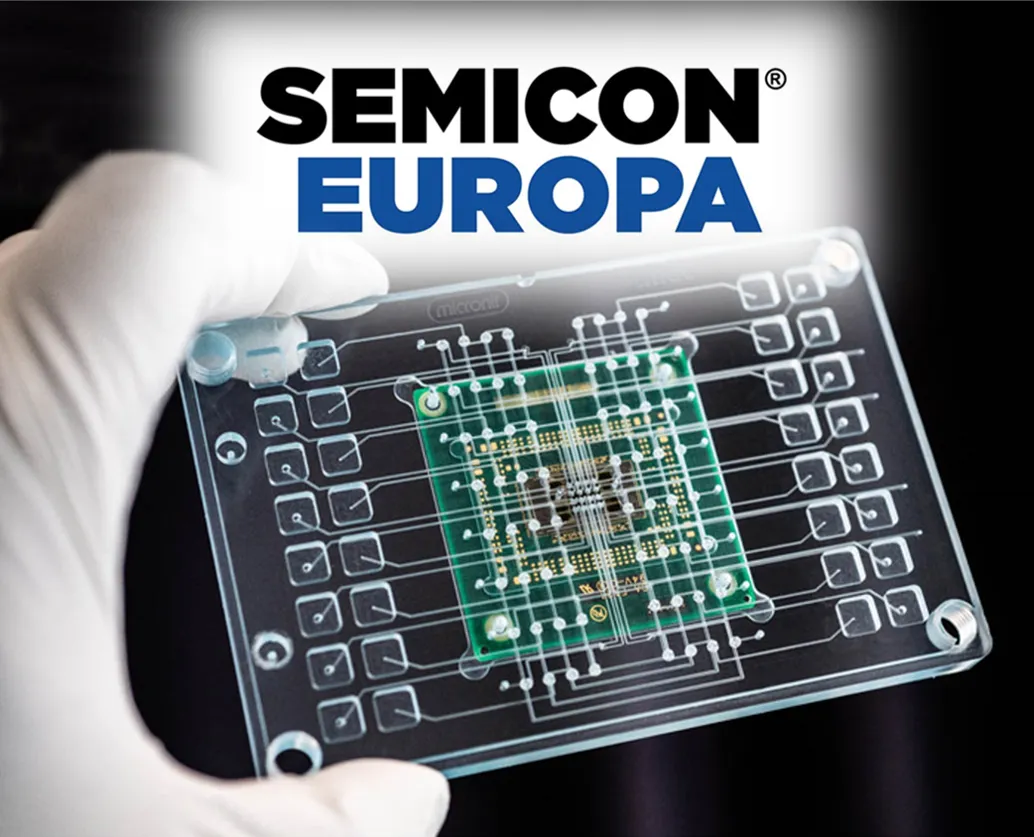
Healthcare has traditionally focused on one-size fits-all medication to treat populations instead of tailoring treatments to individual patients. Recent advances in stem cell technology allow researchers to create disease models for personalized medicine. SEMI spoke with Thomas Pauwelyn, Postdoctoral Researcher at imec, about trends in medical technology innovation such as organ-on-chip devices and their applications. Pauwelyn shared his views ahead of his presentation at the SEMI SMART MedTech Forum, 13-14 November, in Hall B2 (Inspiration Hub) at SEMICON Europa, 12-15 November, 2019, in Munich, Germany. Join us at the event to meet experts from imec.xpand and other key industry influencers. Registration is open. Participation is free of charge for SEMICON Europa visitors. SEMI: What triggered the healthcare move from a one-size fits-all medication to treat populations to tailored treatments? What advancements allowed researchers to create models for personalized medicine? Pauwelyn: One of the main triggers for this transition is the inefficiency of the current healthcare system. The top 10 highest grossing drugs in the U.S. are effective for only between 1 in 25 to 1 in 4 patients. Not only do most medicines only help a small share of the patients, but they are often developed in classical clinical trials with predominantly western or male participants.Recent advances in stem cell technology allow researchers to create disease models for individual patients. In other words, researchers can reprogram cells from a patient’s skin or blood sample to various cell types, including cardiac or neuronal cells, through stem cell techniques. These samples reflect the traits that make a patient unique.However, patient-in-a-dish models expose cells to very artificial environments. So these models look very different from their counterparts in the body. Organ-on-chip systems address these issues by exposing cells to physiologically relevant conditions and create more mature models. SEMI: What is exactly an organ-on-chip? Pauwelyn: Organ-on-chip devices are microfluidic cell culture chips that can revolutionize the development of drugs and personalized treatments. These devices model the pathophysiological behavior of organs and tissues. Inside these chips, cell cultures are grown and exposed to conditions that better resemble in vivo microenvironment. Different organ models can be created by exposing different cell types to an engineered microenvironment. Common examples are the heart-on-chip, lung-on-chip, gut-on-chip or brain-on-chip.SEMI: Medical technology has made astonishing advances over the years. As new medical devices emerge, what are the main challenges?Pauwelyn: Meeting stringent regulatory requirements is one of the main challenges for medical devices. Technologies related to personalized medicine do not neatly fit in existing health technology assessments and reimbursement processes.In the case of organ-on-chip devices, there are challenges related to production, qualification and adoption. Increased standardization will also help scientists compare and interpret their findings. Currently, various research groups obtain different results from own organ-on-chip systems. These systems may be fabricated from different or exotic materials, expose cells to different microenvironments or rely on other cell models. Often, only a few devices are available for testing due to limited fabrication scalability.SEMI: What did imec do to overcome those challenges?Pauwelyn: imec turned to its expertise in chip design and technology to develop a novel organ-on-chip platform in close collaboration with Micronit Microtechnologies in the InForMed project funded by the ECSEL Joint Undertaking (ECSEL2014-2-662155). The platform’s main requirements were that it could reduce handling variability by microfluidic automation, be fabricated with conventional materials compatible with production upscaling, and produce high-quality electrical recordings of cellular activity. Another essential requirement was the compatibility of the device to the standard workflow of pharmaceutical research. The user interface is based a conventional 96-well plate, and peristaltic pumps are integrated into the device.SEMI: How does the CMOS-based microelectrode array work and where do you see potential for applications in the field of personalized medicine?The imec-developed CMOS-based microelectrode array is the sensor in our organ-on-chip system that monitors the cell culture. The sensor consists of 16,384 electrodes distributed over 16 independent microfluidic wells. It detects cellular activity down to the single-cell level, including intracellular action potentials or extracellular signals from electrically active cells or impedance caused by cells growing directly over the electrode.We believe this technology has great potential for developing miniaturized patient models in the lab. By using patient cells reprogrammed to the desired cell types through stem cell technologies, we can develop patient-on-chip systems. These systems would be able to predict which treatment is best suited for a specific patient or how drugs affect certain subpopulations.SEMI: What are your expectations for the SMART MedTech Forum at SEMICON Europa 2019 in Munich? Pauwelyn: The SMART MedTech Forum brings together an interesting mixture of researchers, entrepreneurs and stakeholders in the future of healthcare. I look forward to hearing their perspectives and to discuss how personalized medicine and MedTech will help tackle current challenges.SEMI: Can you share one prediction for the future of MedTech? Pauwelyn: I believe that MedTech in the future will help us tailor treatments to each patient. Doctors will have a wide arsenal of tools available to predict which treatment will deliver both the highest chance of success and the lowest chance of adverse reactions. One of these tools could be a human-patient-on-chip system. It would consist of interlinked organ-on-chip modules with patient-derived cell models. In this way, the reaction of patients to specific treatments could be predicted without ever exposing them to potentially harmful compounds.Dr. Thomas Pauwelyn currently is a post-doctoral researcher with an Innovation Mandate grant from VLAIO, investigating strategies to valorize the results from his research. Pauwelyn’s research focuses on developing novel organ-on-chip systems for predictive toxicology and drug development. He also investigates how organ-on-chip devices may help stratify patients and help enable personalized medicine. Pauwelyn has studied at KU Leuven, Belgium, since 2008. He earned his BSc in Bioscience Engineering specializing in Catalytic Technologies in 2011 and a Master’s in Nanoscience and Nanotechnology with the Bioscience Engineering option in 2013. He completed an IWT fellowship for a PhD at KU Leuven and imec’s Life Science Technologies group in 2018.Serena Brischetto is senior manager, marketing and communications, at SEMI Europe.
Read More
The microelectronics industry is entering the era of Cloud Engineering Simulation to slash the costs and risks of new technology development and speed time-to-market in spaces like semiconductors, MEMS sensors, RF front ends, biomedical and driverless cars. In the run-up to SEMICON Europa, 12-15 November, 2019, in Munich, Germany, SEMI spoke with Ian Campbell, CEO of OnScale, about the new paradigm of Cloud Engineering Simulation. Campbell shared his views ahead of the SMART Design Forum, 14 November, 2019, 14:30 to 17:00, in Hall B1, TechARENA 1 at SEMICON Europa. Registration is open. Join the forum to meet experts from OnScale and other key industry influencers. Attendance is free of charge for all SEMICON Europa visitors.SEMI: How did your adventure with OnScale start?Campbell: I’m an engineer. When I was still in high school, I took a night class at Nashville Tech to learn AutoCAD R14, and I’ve been designing and engineering things ever since. I was introduced to Desktop Simulation in my bachelors of mechanical engineering program and used many types of simulation tools for massive design studies at the Aerospace Systems Design Lab at Georgia Tech. I’m a simulation junkie.I started my first Silicon Valley high-tech company, NextInput, in 2012 with Dr. Ryan Diestelhorst (now VP of Strategy at OnScale), to commercialize new ForceTouch and 3D Touch technologies based on our patented MEMS force sensors. At NextInput, we bought hundreds of thousands of dollars of engineering software, but were always frustrated by slow, inaccurate engineering simulation results. We dreamed about running massive simulations on Cloud Supercomputers and creating true Digital Prototypes that could replace costly, time-consuming, and risky physical prototypes.When I got the chance to join the team that became OnScale in 2017, I jumped at the opportunity. At OnScale, we took engineering simulation solvers that had been developed for the U.S. military to run on U.S. Department of Defense and DARPA supercomputers and built a cloud supercomputer platform on Amazon Web Services to run the solvers. The net-net is the world’s first on-demand, infinitely scalable Cloud Engineering Simulation platform. Now, we routinely run massive multi-billion degree of freedom simulations for Fortune 100 companies, including many from the semiconductor and MEMS industries. Since our business model is to charge per core-hour for simulations, the incredible capability we built is cost-effective and available to small startups as well. SEMI: How is the semiconductor design ecosystem evolving? How is Cloud Engineering Simulation applied to semiconductor and design industries?Campbell: The entire industry is experiencing a massive acceleration in product launch cycles and increased competition. New markets like IoT and 5G are reducing semi/MEMS product cycles from years to months. That, in turn, puts enormous pressure on semiconductor and MEMS designers. Missing a key product introduction like a flagship smartphone launch can literally make or break a company.A reliance on traditional engineering methods – schematic capture and layout of a chip, taping out (physically prototyping the chip), performing engineering validation on an e-bench, qualifying the chip (or not qualifying it and going back to the drawing board), and finally launching mass production – is no longer sustainable from a competitive perspective.Instead, market-leading firms are turning to Cloud Engineering Simulation and Digital Prototypes to explore massive design spaces, find optimum designs that beat the competition in every KPI (size, power, performance), and digitally qualify designs before ever cutting silicon, ensuring that designs are robust over their intended operating environments and performance envelopes. Large thermal analysis of a chip on a circuit board executed quickly on the OnScale Cloud Simulation Platform SEMI: Can you give us an example? Campbell: A great example is thermal analysis. Thermal effects have always had huge impacts on MEMS device performance and, more recently, they are beginning to impact performance of next-gen semiconductors, especially GaN power electronics for electric vehicles (EVs).Conducting a full system-level thermal analysis of something like an EV power management system – a power IC in a package, on a board, in an enclosure, under various loading conditions – has been a challenge from a simulation complexity perspective (degrees of freedom) and from a parametric sweep perspective (running hundreds or thousands of simulations to optimize chip placement, routing, etc.). To run these sets of simulations using legacy desktop simulation would take weeks, perhaps even a month or more. To run these massive simulations in parallel on cloud supercomputers using OnScale takes days or even hours.Our customers routinely run very large simulation studies on OnScale Cloud for thermal simulations, RF filter simulations, MEMS simulations, packaging simulations (what we call Digital Qualification), and many more use cases.SEMI: What’s one of your strategic objectives for 2020? Campbell: For 2020, we’re doubling down on MEMS and semi simulation capabilities. We will be launching additional solver capabilities like EM that will be critical in our strategic markets like 5G. We will also be launching a Cloud API so that engineers can integrate OnScale directly into their existing engineering workflows (e.g. MATLAB or EDA/CAD tools) with just a few Python commands.SEMI: Can you share one prediction for the future of semiconductor design solutions? share?Campbell: I think we will continue to see MEMS and semi designers push the envelope and bring smaller, more performant, more cost-effective solutions to market. I’d like to see more highly cost-effective flexible semi/MEMS designs come to market to enable next-gen IoT and IIoT applications. I’d also like to see more biomedical applications – biomems, microfluidics, and labs on a chip for all sorts of life-enhancing applications.SEMI: What are your expectations regarding the SMART Design Forum at SEMICON Europa 2019 in Munich? Campbell: I’m looking forward to getting back to my roots in MEMS/semi design and chatting with other designers about the future of engineering and the future of semi! Ian Campbell is a twice venture-backed Silicon Valley CEO and expert in MEMS sensors, semiconductor technology, and engineering software. Most recently, Ian co-founded OnScale, a Cloud Engineering Simulation startup backed by Intel Capital and Google’s Gradient Ventures. OnScale is revolutionizing engineering by combining world-class multiphysics solvers with Cloud supercomputers, machine learning, and artificial intelligence. Prior to co-founding OnScale, Campbell served as founder and CEO of NextInput, where he led the startup through multiple rounds of funding – totaling $12 million and an additional $4 million in research contracts with government and industry partners – and built a world-class team of engineers and scientists who developed 3D Touch and ForceTouch technologies for smartphones, wearables, industrial, and automotive interface applications. He also secured the first major smartphone OEM design wins in Asia. Campbell earned his B.S. in mechanical engineering from Middle Tennessee State University, and his MSAE in aerospace engineering and MBA from Georgia Institute of Technology.Serena Brischetto is senior manager, marketing and communications, at SEMI Europe.
Read More
Automotive original equipment manufacturers (OEMs) and their direct suppliers of parts and systems share a vision: Next-generation vehicles will be more electric, autonomous and connected. At a market size of more than $1 trillion, automotive is steadily becoming a high-tech market as cars morph into advanced technology platforms with partially or fully autonomous features. Call them semiconductors on wheels. Big players such as Google and many carmakers are investing heavily in chip advances to help drive increases in silicon content in automobiles.At SEMICON Europa, Pierrick Boulay, Solid State Lighting and Lighting Systems analyst at Yole Développement, will provide a market update on autonomous automobile trends including the state of sensors, radars, cameras and LiDARs as the industry works to increase the level of autonomy and electrification.Autonomous vehicle design can only thrive with the development of an industry standard for chip and device traceability across the supply chain. The importance of chip traceability to the automotive industry is reflected in its central role in driving a chip traceability standard.According to Heidi Hoffman, senior director of technology communities marketing at SEMI, “chip traceability is one of the next big things for the technology industry. The benefits are enormous, and the upsides – including yield enhancements, counterfeiting safeguards, and support for new applications – are plentiful. But the implementation challenges of chip traceability are also big and will require considerable effort to overcome. The biggest hurdle of all? We need to transcend industry fears by demonstrating that we can secure IP when it is shared across the hardware supply chain.” The Importance of Standards, Data Collection and Collaboration Across the Supply ChainThe automotive industry has long embraced tracing the sources of defects. Now, as the automotive and semiconductor supply chains increasingly overlap, traceability has taken on greater importance in the semiconductor industry. SEMI committees, task forces and events such as the Smart Transportation Forum at SEMICON Europa are ideal platforms for collaborating to develop new standards and best practices for the automotive industry.Earlier this year, German luxury automobile maker Audi AG became the first automotive original equipment manufacturer (OEM) to join SEMI as member, strengthening alignment across automotive supply-chain segments. At SEMICON Europa, the SMART Transportation Forum and Pavilion, staged by the SEMI Global Automotive Advisory Council (GAAC) and bolstered by the Electronic System Design Alliance, a SEMI Strategic Association Partner, will gather key stakeholders across the automotive value chain, from design and semiconductor equipment to materials and carmakers, to explore innovation opportunities in automotive electronics. SEMI Global Automotive Advisory Council (GAAC) “If the industry wants to reach the goal of zero defects, a new collaborative approach is necessary,” observed Antoine Amade, senior regional director EMEA at Entegris. At SEMICON Europa, Amade will present new ways to collaborate in reducing chip defectivity and meet other challenges in the automotive industry.More than half of semiconductor failures on the automotive assembly line today (so-called 0km failures) are traced to semiconductor fab defectivity. “The increasing semiconductor content in automobiles – driven by growth in ADAS, electrification and autonomy – has put a growing focus on the quality and reliability of these devices and their implications for consumer safety and satisfaction,” said Oreste Donzella, senior vice president and CMO at KLA.The smart manufacturing (Industry 4.0) revolution is already spurring higher performance and great efficiencies throughout the supply chain and will also be crucial to driving innovation in automotive. Smart manufacturing makes possible significant improvements in factory key performance indicators (KPI) for cycle time, on-time delivery, overall equipment effectiveness, cost and product quality.“These KPI gains are key to meeting quality levels the automotive industry must reach to support the deployment of autonomous driving vehicles,” said John R. Behnke, general manager of Final Phase Systems at INFICON. In his talk at SEMICON Europa, Behnke will provide an overview of existing, in-progress, and future smart manufacturing solutions for the semiconductor industry and their impact on the automotive supply chain. The SMART Transportation Forum, 13 November, 2019 (9:30-15:30 at ICM Munich, room 14c) at SEMICON Europa is the premier platform for key stakeholders to connect, collaborate and innovate across the automotive value chain. Automotive and semiconductor industry experts will offer insights into trends in design, semiconductor equipment and materials, and automotive innovation and the roadmap to 2030. The SMART Transportation Forum will also showcase innovations in imaging, sensing, artificial intelligence (AI), smart manufacturing and L5 mobility.Other SEMICON Europa highlights: Advanced Packaging Conference: Packaging and Test Challenges Towards High Reliability (12-13 November 2019) 23rd Fab Management Forum: Game Changers for Semiconductor Operations(11-12 November 2019) Strategic Materials Conference: Strategic Materials Enabling Industry Roadmaps(12-13 November 2019) SEMICON Europa registration is open for visitors and exhibitors. For more details, please visit the SEMICON Europa website and connect with SEMI Europe on Twitter or LinkedIn @SEMIEurope (use #SEMICONEuropa).Learn more about the SEMI chip traceability standard – SEMI T23 - Specification for Single Device Traceability for the Supply Chain – and SEMI Technology Communities.Serena Brischetto is a marketing and communications manager at SEMI Europe.
Read More