downloadGroupGroupnoun_press release_995423_000000 copyGroupnoun_Feed_96767_000000Group 19noun_pictures_1817522_000000Member company iconResource item iconStore item iconGroup 19Group 19noun_Photo_2085192_000000 Copynoun_presentation_2096081_000000Group 19Group Copy 7noun_webinar_692730_000000Path
Skip to main content
Default Banner Image

pandemic

AEM Holdings Ltd, a Singapore-based multinational corporation, is listed in Forbes Asia’s 200 Best Under A Billion 2019 and 2020 spotlighting small and midsized companies in the Asia-Pacific region with sales under $1 billion. AEM clinched the Singapore Business Review Technology Excellence Award 2020 for Analytics-Semiconductor and the Singapore Business Awards Enterprise Award 2019/2020. These achievements are testament to AEM’s vision and innovation and the company’s contributions to the increasingly complex testing of chips in a rapidly evolving technological world. I spoke with AEM CEO Chandran Nair, a new Regional Advisory Board (RAB) member of SEMI Southeast Asia, about the company’s intelligent test and handling solutions, its role in digital transformation, the company’s key role in the smart manufacturing movement and the growth prospects for Singapore’s electronics sector. SEMI: AEM’s application-specific, intelligent system test and handling solutions for semiconductor and electronics companies serve the advanced computing, 5G and AI markets. How do you differentiate your solutions from those offered by competitors? Nair: A key differentiation for AEM is that we work closely with our customers to develop application-specific integrated test and handling solutions that meet their needs in a scalable manner from lab to production. We offer our customers customized, full-stack test and handling solutions that give them the agility to accelerate their delivery cycles and enhance product quality. Over the years, AEM has developed and acquired world-class technologies in instrumentation, test, automation, robotics, optical inspection, high-end thermal control, and software. These technology pillars, along with our deep know-how to customize test and handling solutions using the technology pillars as a platform, enable AEM to meet the fast-changing needs of our customers faced with the challenges of testing heterogeneous and complex devices. In addition to investing in technology, AEM has also invested in delivering application-specific solutions to meet customer demand. Our recently announced acquisition of CEI with its manufacturing capabilities in Vietnam and its specialization in low-volume, high-mix manufacturing increases our geographical reach and our ability to quickly turn application-specific test and handling solutions to be deployed. We have a unique and differentiated approach that enables our customers to test high-performance computing devices, automotive devices, and mobility devices with maximum test coverage, cost-effectively, in a manufacturing environment. Our experience in serving the high-performance computing market that traditionally drives advancements in thermal control also puts us at the forefront of delivering comprehensive thermal management, vision, and deep automation and test solutions for the computing, automotive, and mobility markets. AEM also has a strong instrumentation portfolio, including high-density digital instruments and mixed-signal and protocol-aware instrumentation that is well-suited for ATE solutions for SoC, high-power devices, and CMOS image sensors. Over the last few years, we have also established leadership positions in developing and deploying application-specific test solutions for MEMS devices and offering wafer and frame probing stations suitable for R D, wafer sort, and final test. We form strong partnerships with our customers, provide them with end-to-end support in product development, and take them through the entire life cycle process from concept to mass production. Chandran Nair and Goh Meng Klang, vice president of operations, at the AEM manufacturing site in Singapore. (Photo credit: AEM) SEMI: Digital transformation is powering strong growth of advanced computing, 5G and AI. Will AEM be expanding its AEM manufacturing plants in China, Malaysia and Singapore to meet rising demand for these technologies in the coming years? Nair: In regards to manufacturing, AEM currently has manufacturing facilities in Singapore, Malaysia, the U.S., Finland, and China. With our recently announced acquisition of CEI, we will add manufacturing capability in Vietnam and Indonesia. AEM will continue to expand manufacturing appropriately to give our customers cost-effective solutions while maintaining our proven track record of delivering on time and scaling rapidly in times of crises like the pandemic or geopolitical disruptions. As for advanced technologies, the three key factors that will bring the full potential of 5G to fruition are 1) cost-effective, high-powered processing devices at the edge, 2) easy access to high-bandwidth communications, and 3) cost-effective sensor technology. Semiconductors are the primary drivers of these three key success factors. As devices become more complex and our reliance on semiconductor-powered devices in all aspects of our lives deepens exponentially to include mission-critical applications, AEM’s role is to ensure that our customers' electronic and semiconductor devices are shipped thoroughly tested, safe to use, and highly reliable. It is imperative that, as a testing company, we find innovative ways to help our customers test their products with maximum coverage and minimum cost. To do this, we are focusing our R D efforts and investments to continue building on our key technology pillars to ensure that we stay ahead of the curve when it comes to test and handling solutions. We prepare our customers to test increasingly complex devices manufactured on the latest process node. SEMI: During your career you’ve driven projects in test and automation and more recently robotics solutions for ports, logistics warehouses and transport. With robotics and automation a key part of Industry 4.0, what role do AEM solutions play in powering the smart manufacturing movement? Nair: The smart manufacturing movement is powered by semiconductors, software and increasingly by artificial intelligence (AI). Test is at the heart of the process of ensuring that semiconductor and electronics devices reach the consumer well-tested for reliability. With our vision of enabling A Zero Failure World, AEM addresses the necessity for safe, highly reliable devices. The semiconductor companies themselves are adopting smart manufacturing methods. AEM’s tools are Industry 4.0-ready, and we continue to invest in machine learning and data analytics, which are integral to the future of test. Our tools are automated and feature embedded sensors to provide our customers with data about tool usage, the state of a machine’s health, and more. Our tools are connected to our customers’ manufacturing automation platforms. Additionally, we continue to invest in our ability to better slice and dice test data to understand trends and patterns to help our customers analyze data and make decisions faster. SEMI: You also have experience heading autonomous vehicle projects. With the COVID-19 pandemic hastening digital transformation, do you see an acceleration in the development of fully autonomous vehicles and smart manufacturing? Research and development efforts for autonomous vehicles (AV) continue at a fast pace worldwide. With shutdowns and restricted movement rules globally, the pandemic has hastened digital transformation in many ways. The delivery of goods and services is transforming, and AV will surely play a part, especially in secure environments for autonomous transport. The pandemic has accelerated the development of autonomous vehicles and smart manufacturing technology in automation-friendly environments like factories and ports. SEMI: At the recent Global Technology Summit hosted by SEMI, you spoke about testing innovations to meet the demands of highly complex devices. Please elaborate on innovative testing solutions versus traditional testing? Nair: AEM offers a disruptive and differentiated solution, one that is driving a paradigm shift to asynchronous, modular, highly parallel, smart testing solutions. ​ The traditional approach of ATEs to test increasingly complex devices on advanced nodes has reached a point of diminishing returns as it gets exponentially more expensive to increase test coverage to acceptable levels. Additionally, as devices get more complex and companies are rapidly adopting heterogeneous packaging technologies, the realization that System Level Test (SLT) is necessary is forcing a rethink of the entire test process. AEM’s provides asynchronous, modular, highly parallel test cell solutions that enable each test cell to run SLT, final test, or burn-in all in one system and its ability to handle hundreds of test cells independently with each test cell testing multiple devices. Our solutions suddenly make comprehensive testing of every complex device cost-effective. Freeing us from legacy ATE allows AEM to provide these innovative solutions to our customers. AEM engineering and manufacturing teams in Singapore at work on semiconductor test and handling systems for global deployment at world-class semiconductor facilities. (Photo credit: AEM) SEMI: Singapore seems to be in the sweet spot of digital transformation. Singapore’s industrial production grew 8.6% year-over-year in January 2021, an expansion driven mainly by a surge in sectors including electronics, and more growth is seen in the year ahead. Digital technologies such as 5G technology and cloud computing together with continued demand for work-from-home equipment is behind this growth. What are the growth prospects for the region’s electronics sector? Nair: Singapore is well-poised to benefit from the current digital transformation accelerated by the adoption of these technologies during the pandemic. Being a safe, well-governed country with strong IP protection, excellent infrastructure, and the rule of law, Singapore is in a great position to play a central role in cloud-based services, 5G, and the semiconductor industry. Singapore’s semiconductor sector output is at a record high, and the prospects for renewed growth in the region are very good. SEMI: As a new Regional Advisory Board member of SEMI Southeast Asia, how is your industry experience relevant to the scope of this role? What opportunities lie ahead for the region? Nair: I am honored to represent AEM in the SEMI’s Southeast Asia RAB. The SEMI RAB can influence policymakers with ideas and information on the current and future needs of the industry. I also believe that SEMI Southeast Asia can cultivate a strong innovative semiconductor ecosystem that helps regional and global growth. I look forward to working with other very experienced and accomplished board members. Bee Bee Ng is president of SEMI Southeast Asia.
Read More
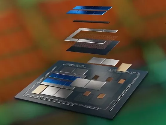
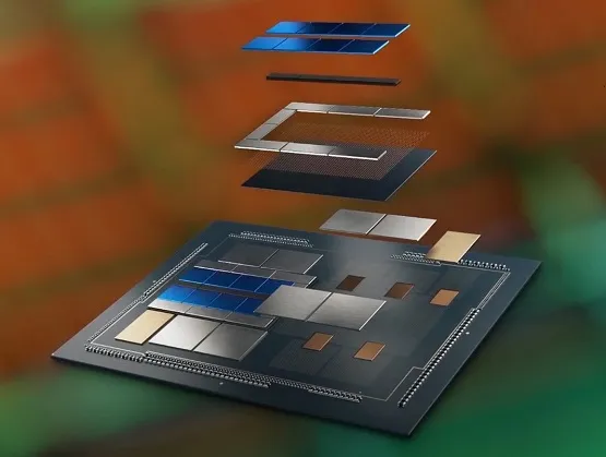
As monolithic scaling slows down, the semiconductor industry is increasingly relying on advanced packaging technologies to extend Moore’s law through heterogeneous integration. Higher on-package bandwidth, improved yield resiliency and the need to integrate diverse IP from multiple foundries are driving demand for advanced packaging technologies that address these issues but introduce challenges of their own such as efficient power delivery to all the different domains in a heterogeneous system. SEMI spoke with Kaladhar Radhakrishnan, Intel Fellow at Intel, about heterogeneous system integration trends and new developments in the semiconductor industry. Radhakrishnan shared his views ahead of his keynote at the SEMI Connecting Heterogeneous Systems Summit, 1-3 September 2021, an online event. Join the summit to meet experts from Intel and other key industry influencers. Registration is open. SEMI: What is driving the adoption of electronics and semiconductor devices nowadays and why is the development of new and innovative technologies important? Radhakrishnan: We are living in an increasingly data-driven world where devices have become an integral part of our lives. A recent study estimated that in the United States alone, 13.6 connected devices per capita consume an average of 300 gigabytes worth of data every month. In the workplace, COVID-19 has driven fundamental business changes that has sped up the adoption of digital technologies such as virtual conferencing, remote work, and e-commerce. Organizations are realizing that a high-quality video conference can be an adequate substitute for many in-person meetings. As a result, businesses are accelerating the digital transformation in order to adapt and thrive in this new environment. Five decades of sustained exponential growth in semiconductor performance has conditioned the average digital consumer to expect more from their devices. However, there are some headwinds ahead as traditional scaling slows down and power density rises. Because consumers and businesses are now generating data at a faster rate than they can consume it, technologists need to scale compute, storage, and bandwidth even faster to keep pace. Without investments in research and development of new and innovative technologies to address these challenges, the full potential of this data will go unrealized. SEMI: What forces are heightening the importance of heterogeneous system integration? What are the implications for increased on-package bandwidth, improved yield resiliency and the need to integrate diverse IP from multiple foundries? Radhakrishnan: The semiconductor industry increased transistor density and scaled performance through classical Dennard scaling until the turn of the century. By then, the gate oxide thickness had scaled down to atomic dimensions and the exponential increase in sub-threshold leakage signaled the end of scaling through traditional methods. Since that time, the chip industry has been relying on innovations in transistor materials and structures such as high-k metal gate, strained silicon, and FinFETs to keep pace with Moore’s law. However, this alone will not be sufficient to continue scaling and the industry needs to explore other vectors to augment improvements in transistor technology. Heterogeneous integration through advanced packaging is one key technology that can help drive these gains. Technologies like Foveros can enable device density scaling by creating a 3D stack of multiple die using high-density interconnects. Heterogeneous integration enables chipmakers to move from a monolithic system designed on a single large chip to a heterogeneous system comprised of a number of smaller chiplets. The main benefit of using smaller chiplets is that they improve yield and enable application based customization of the foundry processes. However, if the disaggregation to smaller chiplets is not accompanied by an increase in on-package bandwidth, the power and performance penalties associated with chiplet-to-chiplet communication will hobble system performance. This is why advanced packaging technologies that improve die-to-die communication are key enablers for heterogeneous integration. SEMI: What are some of the key technology challenges in developing heterogeneous systems? Radhakrishnan: The obvious challenge that most people focus on is the need for improved on-package bandwidth. However, as we rely on 3D stacking to continue device scaling at the package level, it is important to comprehend power delivery and thermal challenges as well. Power to the top die has to be delivered through TSVs on the bottom die, which not only adds resistance but also reduces the useful area available on the bottom die. This problem is further exacerbated when we stack more than two die. Excessive noise on the power delivery network can cause timing issues that limit the maximum operating frequency of the transistor. Similarly, when we stack multiple die, we must take into account associated thermal challenges. For example, each interface of the multi-die stack adds thermal resistance, which makes it harder to cool the chips at the bottom. SEMI: What are some of the key global market trends that driving demand for heterogeneous and system-level integration? Radhakrishnan: The number of artificial intelligence (AI) and machine learning applications have grown dramatically due to their ability to solve highly complex problems across a wide range of segments. AI and machine learning models require more memory bandwidth and compute capabilities that are difficult to achieve without some form of heterogeneous integration. Another market trend driving demand for heterogeneous integration is the increasing reliance on custom hardware accelerators. To combat the slowdown in frequency scaling and single-core performance, we have moved to multi-core architectures by tackling the inherent parallelism in our workloads. However, Amdahl’s law tells us that such an approach will hit a bottleneck when we reach the limits of the serial portion of the workload. As these constraints slow the performance of general-purpose processors, the reliance on custom hardware accelerators to boost performance for specific workloads is growing. Heterogeneous integration at the system level with a combination of CPUs, GPUs, FPGAs and other accelerators can optimize system power and performance. SEMI: What solutions is Intel developing to address these market needs? Radhakrishnan: Intel is actively involved in the development of the industry ecosystem for heterogeneous integration. We have developed a number of innovative advanced packaging solutions such as the EMIB and Foveros that are used in products today. Intel is also developing the next generation of advanced packaging technologies, Foveros Omni and Foveros Direct, which will dramatically scale the IO density by using direct Cu-Cu bonding technology. Foveros Omni is a crucial building block technology to enable high-voltage power conversion on the package for efficient power delivery. Intel is uniquely positioned to predict the design needs for future systems and deploy its resources to develop the technology building blocks needed to continue performance scaling. Our IDM 2.0 strategy enables us to leverage our leadership in packaging technologies to design the best products and use the best IP to deliver leading products across a broad range of categories. SEMI: What do you expect from your participation at SEMI Connecting Heterogeneous Systems Summit? Radhakrishnan: I’m hoping to shed some light on some of the new technologies we have been developing at Intel to enable heterogeneous system integration. I also want to bring awareness to the power-related challenges we are facing with heterogeneous systems. I also look forward to listening to what other industry leaders have to say on the topic. Kaladhar Radhakrishnan is an Intel Fellow and a Power Delivery Architect with the Technology Development group at Intel. He plays a significant role in shaping and driving power delivery technologies for Intel microprocessors. His areas of expertise include integrated voltage regulators, advanced packaging and passives technologies. Kaladhar is a two-time recipient of the Intel Achievement Award, the highest Intel honor an individual or small team can receive. He has authored four book chapters, over 40 technical papers in peer-reviewed journals, and has been awarded 35 U.S. patents. He has also served as an adjunct professor at Arizona State University. Kaladhar joined Intel in 2000 soon after receiving his Ph.D. in Electrical Engineering from the University of Illinois at Urbana-Champaign. Serena Brischetto is senior manager of marketing and communications at SEMI Europe.
Read More
COVID-19 has likely had a greater impact on healthcare than on any other industry sector, said Glenn Snyder, Principal and Lead Analyst for MedTech at Deloitte, and a featured speaker at a recent SEMI webinar that offered a glimpse into the Future of MedTech in the run-up up to the SEMI Global Smart MedTech Symposium, kicking off tomorrow and running through August 5th. Snyder said medtech growth may appear muted in its early years but is poised to begin a steep climb as innovation continues, harkening back to the super-charged growth of circuitry on a wafer (aka Moore’s Law), which also saw a seemingly slow, flat start. Medtech enjoy its own exponential growth powered by 5G implementations, consumer demand, and the development of a robust ecosystem of bio-sensors, data standards, and regulatory improvements. Consumer-Driven Future and COVID-19 Impact Snyder noted that the future of medtech will be consumer-driven – enabled by open, highly interoperable data and secure platforms geared toward end users. A case in point: Detecting disease early through sensor systems will rely on not only on-body and environmental sensors, marking a fundamental shift from the today’s today’s hospital-centric system to improve health outcomes. Telemedicine growth during the pandemic is a notable example. In one case study of a health system, Snyder noted that telehealth usage skyrocketed from 1% to 60% of all patient visits over the early months of the pandemic but has since dropped to 10% due to the lack of charting, billing and other support systems needed to sustain the high rate of telehealth visits. Even so, hospitals expect to see a steady rise in consumers’ use of telehealth in the coming years. One driver are pilot programs for healthcare-at-home services for post-surgical patients. The programs have delivered better health outcomes and are more personalized and family-friendly than medical clinic or hospital visits. They also cost less. Digital monitoring using remote biometrics sensors are one key to driving the long-term success of these programs. Health Systems Changing Their Business Model In the medtech sector, changes in health system business models lag consumer adoption. What’s more, policy changes aren’t keeping pace with new models for medtech products. For medtech products to thrive, a solid foundation of data gathering, transmission and management capabilities that tie into traditional healthcare systems must be formed. Companies considering a vertically integrated approach to the medtech market can steer clear of healthcare providers – but only at the risk of having less access to patients and their historical healthcare data. Snyder said companies that control vertically integrated healthcare products and patient data can make support systems more efficient and robust but may struggle to deepen their market penetration. Companies such as Intuitive Surgical have found success with this model by offering highly differentiated products. Supply Chain Alarmingly Thin for Medtech Devices In a recent Deloitte survey of medtech companies, 60% reported that at least half of their products are powered by semiconductors, yet 70% noted pointed to high supply chain risks with most of their products because they have only a single source. Risk management and creating a resilient supply chain will remain key for medtech providers to adapt on a global scale. Partnerships and Collaborations During the event roundtable, Snyder mentioned that bio and pharma companies have partnered successfully to grow their businesses. Doug Kiehl of Eli Lilly, the moderator of the discussion, added that traditional healthcare providers should look outside of their usual business circles for medtech innovation. COVID-19 highlighted how new multi-disciplinary healthcare partnerships risk assessment processes have opened several paths to innovation previously unexplored. Both Snyder and Kiehl expect to see more collaboration between health systems and medtech innovators as they uncover synergistic business models. SEMI Global Smart MedTech Symposium Kicks Off Today Explore the gaps in the supply chain at the Global Smart MedTech Symposium and join the conversation with medtech device companies and health systems providers. Sessions include: Realtime Continuous Diagnostics and Monitoring Decentralized DNA Sequencing and Molecular Diagnostics Data Science and Infrastructure – AI/Data Fusion Applications in Rural and Decentralized Healthcare in the Digital Age The four-day symposium features three sessions at different times each day to cater to participants in Taiwan/Asia, Europe and North America. Register today! Heidi Hoffman is senior director of Technology Communities marketing at SEMI.
Read More
When COVID-19 hit the semiconductor industry, SEMI members were confronted with new hurdles to keeping their employees safe and their operations running uninterrupted. We quickly assisted our global membership around the globe by providing a forum for collecting member insights on best practices for operating and safety procedures, supply chain issues and sentiments on business impact and recovery. That forum took the form of surveys we launched in March 2020. We shared the results with the larger SEMI member community to help them cope with the evolving impacts of the pandemic on their businesses. Following is a summary of our 4th survey, issued last month. Regional and Sector Representation Nearly 40% of our respondents represented companies headquartered in North America. Of the respondents, 10% each were from companies headquartered in Taiwan and China; 5% from Korea, 13% from Japan and 20% from European and Middle Eastern members. The largest share of respondents – 40% – develop equipment for semiconductor fabrication, assembly, and test; 21% supply materials to the microelectronics industry; 14% are device makers; 6% supply software and design services; and 3% are OSATs, EMS suppliers or ODMs. Measures Member Are Taking to Continue Operations The May survey found that almost no companies ceased production for any significant length of time. In order to continue operations, companies instituted social distancing and masking requirements, temperature checks, schedule changes, and some contact tracing, all to varying degrees, as shown in Figure 1. In addition, several companies implemented some combination of mandatory testing, bump sensors, air purification and site capacity limits and sequestered foreign workers in separate housing for required quarantines after travelling. Figure 1 All of these measures are routinely discussed during the regular SEMI EHSS COVID-19 Working Group calls. That group consists of facilities, HR managers and others tasked with ensuring safety monitoring and compliance at member companies. Company Vaccination Policies With the pace of vaccine rollouts varying widely around the world, only 5% of respondents are requiring all workers to be vaccinated before returning to the office, and 12% have not yet considered a vaccine policy. The majority of companies are encouraging but not requiring employee vaccinations, and 26% leave the decision to the individual employees. Figure 2 North American companies constituted the majority of the required and encouraged vaccination categories. In Europe, companies fall into the employee decision or encouraged categories but none require vaccinations. Japanese companies primarily leave the vaccination decision to employees, while Chinese companies are split among the required, encouraged and employee decision categories. Clearly, these guidelines are not required by law in each region, but instead fall to employers and local policymakers. Member Readiness for Digital Transformation A solid majority of members reported they have invested in the adoption of digital transformation technologies and practices, though only about 14% expect to continue their digital investments in the coming year. Many respondents have deployed virtual meeting software and have implemented or plan to put in place virtual reality tools for remote diagnostics and predictive modeling for semiconductor manufacturing. Figure 3 Location by Functional Group in Returning Employees to Sites Not surprisingly, manufacturing and distribution staff that could work from home during the pandemic are back on site, and respondents signaled that R D and engineering groups will soon end their remote work, following by finance and procurement. Sales and marketing show the highest percentage of staff working remotely, with sales having the highest number remaining remote for some time to come. Figure 4 Resilience to Further Economic Uncertainty Of the 274 companies responding, 229, or 84%, feel more resilient in the face of further economic uncertainty after their response to COVID-19, though continuing supply chain issues and raw materials shortages ranked among their top concerns, as did rising customer demands, their ability to increase capacity utilization rates, and the increasing demands on employees and facilities overall. Figure 5 Many thanks to all survey respondents over the past year! We’ll keep you up to date on results of future surveys. For more details on the SEMI EHSS COVID-19 Working Group calls, visit the SEMI COVID Response Site. To watch the recording of our most recent CEO Webinar – Surging Chip Demand, Digital Transformation, and the Pandemic – What’s Next? – click here. More than 750 people attended the June 2nd webinar sponsored by SEMI members Brooks Automation, Hitachi, JCET, KLA and TEL. Heidi Hoffman is senior director of Technology Communities marketing at SEMI.
Read More
As we move through Q2 of 2021, it seems that the world is finally approaching normalcy. But I don’t believe our lives and businesses will ever be the same. Travel is unlikely to return to the same level as pre-COVID-19 for many years. I’m sure many companies will establish tighter travel policies and budgets as virtual conferencing has proven to be beneficial and cost-effective. Patients and doctors who were skeptical of telemedicine are embracing it, and although it’s not perfect, it has filled a needed gap. Online learning essentially happened over a weekend and will now be part of many curriculums and programs. All of these elements have spurred our semiconductor industry into a super cycle. Demand for chips is leading to an increased demand for semiconductor equipment. Semiconductor capital equipment expenditures in 2020 surpassed $63 billion and are forecast to top $70 billion in 2021. The secondary equipment market typically makes up about 5% to 10% of that. Our inquiries have definitely increased this year. With this in mind, I’d like to share some thoughts for the remainder of the year. Storage of Chipmaking Equipment Not New The semiconductor industry has been experiencing an equipment shortage for some time. It is difficult for original equipment manufacturers (OEMs) to support such a large variety of products and technologies. Some companies use equipment for manufacturing 150mm, 200mm and 300mm wafers. Fabs still run 30-year-old technology on 150mm wafers while the latest technology is manufactured on 300mm wafers. We’ve also seen new technologies like silicon carbide (SiC) being developed on these smaller wafer sizes. Unfortunately, some OEMs stopped making 150mm and 200mm some time ago and have only recently jumped back into the market. These OEMs have had to balance technological advances, pricing, and manufacturing capacity to meet this demand since their primary focus is on 300mm equipment. Third-party refurbished equipment suppliers have also experienced an increase in demand over the last several years. We see it increasing at all technology levels over the next three to five years. This translates to increased equipment pricing for both new and used equipment, as well as increased lead times. Growing Demand for Legacy Tools Many electronic products we use and are familiar with don't require state-of-the-art technology. For instance, cellphones, electric vehicles, wearables, monitors and industrial products still contain many chips manufactured on 200mm wafers using 200mm equipment. There are still approximately 200 200mm fabs worldwide and this makes up about 25% of all wafer capacity regardless of wafer size. These fabs manufacture analog devices, MEMS products, power management ICs, RF devices, discrete devices and sensors. We have also seen an increase in lead times for 200mm equipment. Typical lead times of three to six months have increased in some cases to one year or more. This situation has created a dramatic increase in chip making equipment prices and we do not expect much relief there. Many OEMs transitioned to 300mm equipment prior to 2010. Revenue and profit margins are much higher for them on 300mm equipment. 200mm manufacturing was supported by many third parties for a while. However, in 2016 we saw a resurgence in 200mm equipment, and at that time many OEMs began jump-starting their supply chains. It took some time for them to develop new supply chains, upgrade technology and in some cases hire newly trained engineers to support these new tool sets. All this costs money, which is why we will continue to see an increase in new legacy equipment pricing. Because manufacturers and products may not be able to support these prices, we expect the robust third-party ecosystem to continue. SurplusGLOBAL's Response to this Demand One of the advantages we bring to the secondary equipment market is our ability to recycle technology. We continuously search for opportunities to purchase large packages of tools from companies that are transitioning technology nodes, moving from 200mm to 300mm wafer size or changing product lines. We spend approximately $65 million to $100 million each year on purchasing equipment and in some cases storing it for the right customer. For instance, a memory company may be changing technology nodes and no longer needs its equipment. This use to happen on a predictable schedule. Instead of scrapping that equipment, SurplusGLOBAL purchases and stores it. Sometimes we only need to store it for one month before relocating it. However, in many cases, we store it for one year or more. We may power it on at a later date if it is in good condition. In some cases, we work with an OEM or third party to have it refurbished and ready for a new customer. In response to the need for more secondary market equipment, we have opened up additional offices in Japan and Singapore to stay close to and better support our customers in those regions. Finally, our biggest and most recent endeavor is building our Semiconductor Equipment Cluster, which opens in July 2021. Learn more about the SurplusGLOBAL Semiconductor Equipment Cluster. Emerald Greig is executive vice president Americas at SurplusGLOBAL.
Read More
Now, more than ever, semiconductor companies are relying on their human resources departments to ensure employee safety, support facility access and hygiene measures, cope with staffing demands and incorporate the rapidly evolving guidelines from Centers for Disease Control and Prevention (CDC) and the local state and city mandates. SEMI spoke with Crystal Reich, HR manager at X-FAB Texas, about her participation in the Fab Owners Alliance (FOA) human resources group and the value of collaborating with industry peers on a broad spectrum of topics: from focusing on specific areas such as ensuring employee safety and managing the workforce during a pandemic, to addressing broader organizational challenges such as benchmarking activities and identifying compensation and staffing best practices. SEMI: How did you learn about the FOA human resources group? Reich: I have been part of the FOA HR group since its inception in 2012. Lloyd Whetzel, the CEO at X-FAB Texas, has been very involved with the FOA for several years. When this group was being formed, he let me know about it. I came to the first meeting and have been a part of it ever since. SEMI: What does your participation in the FOA human resources group allow you and your company to do differently? Reich: I am also involved with the Society for Human Resource Management (SHRM), but the FOA HR group provides an excellent opportunity for semiconductor industry HR professionals to collaborate. The group not only covers topics that are specific to the semiconductor industry but also discusses broader topics related to preserving employee well-being during unprecedented challenging times, managing negative emotions, establishing appropriate political expression policies, and creating safe spaces for dialogue. Also, the benchmarking has been fantastic, especially from a compensation and staffing standpoint. It allows us to identify best-in-class recruitment strategies, determine any shortfalls and use this information to improve employee onboarding and development. In addition to discussing these types of issues and trends, we compare and benchmark other HR issues such as policy deployment and legislative trends with colleagues in the industry. SEMI: What are some of the key topics and activities that the FOA HR group has helped you focus on? Reich: X-FAB has been involved in a variety of activities at SEMI. Through the SEMI High Tech U program, we have been able to help college-bound high school students in our community access STEM curriculum and explore careers in technology. We have devised more robust military outreach strategies with the help of the Veterans Program at SEMI, allowing us to recruit and retain excellent technicians from the military. Additionally, benchmarking activities within the FOA HR group have helped us improve our talent acquisition process - especially for positions which are challenging to fill. SEMI: The pandemic brought many significant and unprecedented challenges that affected business continuity. How did your company's participation in the FOA help you navigate these changes? Reich: The FOA has been a great help in addressing the challenges of the global pandemic across several operational collaborative teams. In the early days of the pandemic, as employees moved to remote work, FOA organized a forum that allowed members to share how they dealt with this transition. Constantly changing guidelines and protocols meant that FOA members leaned on each other more than ever to share best practices and lessons from new safety process implementations. FOA offered survey and area-specific team activities, cross-functional operational sessions, and round table discussions at its 2020 Q4 meeting, where members exchanged ideas on how business processes changed during this period and shared what they were doing to ensure business continuity. This provided another excellent opportunity for FOA members to benchmark best practices within the semiconductor industry. SEMI: Would you recommend your peers to join the FOA HR group? Reich: I would highly recommend HR colleagues in the semiconductor industry join this collaborative group. It is a great platform to share ideas, learn from each other, and benchmark with other colleagues in the same industry. The FOA HR Metrics survey is a comprehensive survey covering several different areas within the HR discipline such as compensation, learning and development, tool training, corporate social responsibility, and many others. True to the nature of the FOA, the survey is a result of the collaboration between several HR professionals from Device Maker member companies. Please contact Shilpa Talwalkar at [email protected] if you would like to participate. X-FAB is a member of the SEMI Fab Owners Alliance, an international group of semiconductor and MEMS fab managers and industry suppliers that meet regularly to solve common non-competitive manufacturing issues and improve their business results. Nishita Rao is senior product marketing manager at SEMI.
Read More