downloadGroupGroupnoun_press release_995423_000000 copyGroupnoun_Feed_96767_000000Group 19noun_pictures_1817522_000000Member company iconResource item iconStore item iconGroup 19Group 19noun_Photo_2085192_000000 Copynoun_presentation_2096081_000000Group 19Group Copy 7noun_webinar_692730_000000Path
Skip to main content
Default Banner Image

MSIG

Why do we need environmental air pollution sensors?Today we need environmental air pollution sensors more than ever to ensure that we have clean and safe outdoor and indoor air. Although federal rules have improved air pollution over the past several decades, more than 110 million Americans still live in counties where air quality is below national standards. An estimated 100,000 Americans die prematurely each year of illnesses caused or exacerbated by polluted air.“Cars and trucks are much cleaner than they were, power plants are cleaner, industrial operations are cleaner,” said Paul Billings, Senior Vice President Advocacy for the American Lung Association. But cleaner air is not clean air.”While scientists have long known that air pollution may exacerbate asthma and other respiratory illnesses, new data suggests polluted air leads to higher COVID-19 higher death rates and brain inflammation that can contribute to dementia and autism.To understand the importance of air quality and how we can apply existing sensors and develop new ones, we look both outdoors and indoors (see Figure 1). Outdoor air quality relates to gaseous and particulate pollutants, defined by the Air Quality Index (AQI). The AQI became a standard based on regional thresholds for a set of key outdoor pollutants: four gaseous pollutants (sulfur dioxide, nitrogen dioxide, carbon monoxide, ozone) and particulates (PMs) of different sizes such as 10 μm (PM10) and 2.5 μm (PM2.5). At present, the AQI is measured using traditional analytical instruments. Despite their high acquisition and maintenance costs, these instruments are the only solution to accurately measure these pollutants in the presence of variable environmental background.Figure 1. Examples of outdoor and indoor air quality markers Indoor air quality (IAQ) is also of growing concern. Formaldehyde, benzene, carbon monoxide, and carbon dioxide are some of the key pollutants with restricted concentration levels in residential, office and industrial buildings. Sources of these and other gaseous pollutants include building materials and equipment, workplace cleansers, and building occupants. Regulatory agencies and building occupants use different methodologies to estimate IAQ using gaseous and particulate pollutant analyzers. These estimates also consider air humidity and temperature that affect indoor air quality. Where are we today with environmental sensors?The top three requirements for modern gas sensors include: the sensor reliability to provide accurate readings in diverse environmental conditions over desired period of use low power, to extend battery life or to eliminate its need, and low cost, to facilitate their ubiquitous deployments. Advances in electronics, microfabrication, and packaging have delivered recent important developments in reducing the power consumption and miniature packaged solutions. Recent R D efforts are also increasing the number of successful gas sensor field deployments for outdoor and indoor air quality monitoring. Figure 2 illustrates three examples of recent developments in gas sensors that meet requirements of diverse customers.Electrochemical sensors from SPEC Sensors were collocated with EPA instruments for monitoring of NO2 and O3 in Chicago’s Array of Things Project. Figure 2A shows that these new cost-effective sensors track well the EPA instruments. Advancements in circuit quality, sampling, enclosure design, and initial calibration/compensation were all essential in achieving these results. While this example clearly demonstrates the usability of these sensors in this particular application, the expectations that low-cost, off-the-shelf sensors will match the performance of EPA reference systems that cost 50x-100x more must be adjusted. A micropackaged sensor suite from Bosch Sensortec includes sensors for total volatile organic compounds (TVOCs), temperature, humidity, and pressure. TVOC measurements are needed according to the guidelines by the German Federal Environmental Agency. To report TVOC, the sensor algorithm tracks the TVOC-related resistance of the metal oxide sensor, corrects sensor resistance for ambient temperature and humidity, and outputs the TVOCs Index of Air Quality between 0 (clean air) and 500 (heavily polluted air) as shown in Figure 2B. A recent GE-developed dielectric excitation scheme of metal oxide sensing materials provided a highly desired and long-awaited calibration stability of sensors for monitoring of fugitive methane gas emissions in all-weather conditions. These sensors were used in several field validation campaigns in Oklahoma, North Dakota, Arkansas, and British Columbia and had stable performance after more than 400 days, as compared to an initial calibration (see Figure 2C). Such stable sensor performance has become possible by switching from the conventional resistive mode of operation of metal oxide sensing elements to the dielectric excitation scheme. Figure 2. Examples of applications of contemporary gas sensors based on different detection principles.(A) Outdoor performance of NO2 and O3 electrochemical sensors versus EPA-validated instruments.(B) Calibration results of a BME680 metal oxide gas chemiresistor upon exposures to TVOCs (blue stair-profile) and its ± 15% confidence interval band as the Index of Air Quality.(C) Calibration stability of a sensor with an innovative dielectric excitation scheme implemented for monitoring of fugitive methane gas emissions after multiple uses in diverse field validation campaigns. Key challenges and solutions toward realizing new applicationsIn this era of data-on-demand, environmental sensors could enable countless new applications. Imagine you have a gas sensor conveniently integrated into a smartphone or a watch. You are commuting to work, and your sensor alerts you that the subway station through which you are traveling has very poor air quality. How might this alert affect your behavior? Would you put on a mask, change your commuting route to a twice-longer one, or petition the city? What if you are attending a parade downtown with your asthmatic child, and your device informs you that the air is clean? Would you skip the parade if you knew that your sensor was only 10% accurate? How would you avoid a risk of ending with your asthmatic child in a hospital?Design principles of modern sensors originate in the 20th century for detection of high gas levels from leaks, but they did not anticipate the applications proposed now. By design, existing sensors have only a single output – e.g. resistance, voltage, current, light intensity – that mathematically cannot correct for the sensor instabilities caused by the complex chemical background and variable temperature and humidity conditions. Thus, often these simple sensors perform best when pollution levels are high and when the compound of interest swamps others. As a practical example, there are dozens of gaseous pollutants in ambient air with their toxicity that differ 1,000-10,000 fold. Often, the insufficient reliability and accuracy of existing sensors in the field conditions is a significant bottleneck toward the broad adoption of gas sensors. According to the United States Environmental Protection Agency (EPA), the correlation between readings of low-cost sensors versus reference monitors varies widely from 1% to 80%. The EPA also states that no low-cost sensors meet Regulatory Monitoring requirements, and the World Meteorological Organization emphasizes that “low-cost sensors are not currently a direct substitute for reference instruments, especially for mandatory purposes.” However, we now have the increasing number of examples of reliable operation in complex environments (Figure 2) in addition to important advances in reduced power and size of contemporary sensors. Still, the key challenges to realize new applications are often the lack of required accuracy and reliability of available sensors for new contemplated applications.Is it possible to offer low-cost sensors for at least some applications and some gases with the degree of accuracy approaching more expensive specialized instruments? We, the SEMI-MSIG Device Working Group, are saying: Yes. To deliver on this bold statement, our SEMI community brings new technological solutions to the 100-year old general design of gas sensors.Our next blog What is in the Air will provide details on our activities of SEMI-MSIG Device Working Group to establish standards and new measurement schemes to reduce effects from uncontrolled ambient conditions and to improve stability, limit of detection, and dynamic range of environmental sensors. Also learn how new MSIG members can impact this important working group. The MEMS Sensors Industry Group (MSIG) is a SEMI technology community that enables the MEMS and sensor industry to address common challenges, innovate and accelerate business results.Radislav A. Potyrailo is Principal Scientist, Micro Optoelectronics Gas-Chem-Bio Sensors Systems, at GE Research; Ed Stetter is General Manager at SPEC Sensors, LLC; Ryotaro Sakauchi, is Senior Manager of Business Development at Bosch Sensortec; Merry Smith is a Product Manager and Senior Scientist at C2Sense, Inc.; and Sreeni D. Rao is Senior Director of the MEMS Business Group at TDK Corporation.
Read More
A lot has happened in fifty years, particularly when it comes to the microelectronics industry. Founded in 1970 by a group of semiconductor industry pioneers who believed that co-opetition — instead of traditional competition—would produce a more vibrant emerging industry, SEMI was born as an industry association.It's fitting during this week’s 50th annual SEMICON West (July 20-23, 2020) — a virtual event for the first time — that SEMI Chief of Staff Bettina Weiss offers her perspectives on the evolution of SEMI from one of the best seats in the house: the 24 years that she has spent helping the association change and grow.Vetrano: You’ve enjoyed a long rich history with SEMI, and now serve as the association’s first chief of staff. What roles have you played at SEMI up to this point?Weiss: I cut my teeth at SEMI by joining SEMI Standards, first serving as standards coordinator at SEMI Europe from ’96-’97. Over the next 11 years, I held a variety of positions at SEMI Standards, culminating with director of international standards from 2003-2008. Given that experience, I have to admit that SEMI Standards are still near and dear to my heart.I moved on to several leadership positions in our former global photovoltaics/solar business through 2014, and toward the end of that stint, I assumed additional responsibilities, becoming vice president of business development. That’s where I dove headfirst into expanding SEMI into emerging regions, including Vietnam, India and Latin America. SEMI goes where members see (or want to better understand) new opportunities, especially in places that had ambitious plans for fabs for microelectronics, including semiconductors and MEMS.In 2018, I became SEMI chief of staff, reporting directly to our president and CEO Ajit Manocha.Vetrano: Now I hardly know where to start! Since I have to decide, what does it mean to be SEMI chief of staff?Weiss: As the first chief of staff, I’ve been able to shape the position, combining the support of critical efforts driven by Ajit with additional project management responsibilities like our Smart Mobility initiative.Working with experienced leaders in our industry, such as the Board of Industry Leaders (BIL), is one of the more rewarding parts of my role at SEMI. The BIL is a group of global executives tasked with advising SEMI on strategic planning, especially when it comes to future-looking initiatives like Smart Mobility, Smart MedTech, Smart Manufacturing, and Smart Data/AI.A lot of the other things I do are meant to support the whole SEMI organization, in partnership with other senior leaders such as Michael Ciesinski, vice president of technology communities, as we create business plans and examine new revenue models that will keep SEMI sustainable and viable for the future. This includes issues as varied as workforce development and diversity and inclusion, and the new digital platforms we use to engage with our members.Vetrano: How does SEMI Smart Mobility initiative exemplify the model of engaging end customers in vertical markets that are important to members?Weiss: When you look at the rapidly increasing number of chips and sensors in and around vehicles, Smart Mobility at its core brings together both the semiconductor/sensor and automotive/mobility supply chains for a more transparent dialogue about needs and wants along the entire supply chain. We are thrilled to count automotive OEMs Volkswagen and Audi as SEMI members. We also work with Tier 1 suppliers such as Continental and many others to promote the open exchange of ideas and foster collaboration among all stakeholders.Smart Mobility is a good example of how SEMI connects two worlds that are now interdependent for the mutual benefit of all players. Automotive companies and component suppliers want to better understand new technology capabilities that enable tomorrow’s infotainment, safety, security and communication protocols. And semiconductor, sensor and component companies see huge upside in supplying the equipment, materials, devices and subsystems that enable the future of mobility. Smart Mobility is a win-win, and the founding concept of our Global Automotive Advisory Council (GAAC).Vetrano: As we look to COVID-19, the single most important event to influence the microelectronics industry — and every other industry — why is SEMI membership more important now than ever?Weiss: Our industry is facing a triple whammy of challenges: a global pandemic, ongoing global trade tensions that impact interdependent supply chains, and a global economic crisis. All these challenges will require our members’ ingenuity, innovation and collective action to overcome them. But inherent in those challenges are tremendous opportunities, and I have no doubt that our members and the entire global electronics ecosystems will find ways to help everyone prosper and advance.COVID-19 has had a huge impact on our members. From the onset of the pandemic, we’ve provided our members with resources including best business practices, insights and data from industry experts to help them respond to a virus that has already changed so many things we took for granted before March. Additionally, SEMI has also advocated with governments around the world on behalf of the industry for essential business status and essential travel to sustain operations. Visit SEMI COVID-19 Resource page for information on industry best practices and much more.Vetrano: Before we look forward, what has changed dramatically in microelectronics since you started at SEMI?Weiss: Through my work with SEMI, I’ve witnessed dynamic, dramatic and sustained change in the microelectronics supply chain. Into the late 1990s, SEMI represented primarily semiconductor equipment and materials suppliers, and we worked with chipmakers – our members’ customers. That’s where a lot of important Standards work happened, for example, and the supplier-device maker relationship was pretty much our world. Over the years, we saw significant change in how companies partner and do business with one another. The digital transformation we’ve been witnessing for the past few years was the impetus for expanding our reach to bring companies in the extended electronics manufacturing and design supply chain together, from sand to system, so to speak. That was also when we invited associations representing flexible hybrid and printed electronics (FlexTech), MEMS and sensors (MSIG), and electronic system design (ESD Alliance) companies to join SEMI and our other technology communities for maximum cross-pollination. That’s because everything needs microelectronic devices and systems. Vetrano: Looking ahead now, what is can the microelectronics industry do to benefit humanity?Weiss: Semiconductors and sensors are often the unsung heroes of progress. Microelectronics can help bring prosperity to the billions of people now struggling on our planet. It can improve access to education for people through e-learning, it can advance agricultural production and streamline the food supply chain to help feed the world’s hungry, it can monitor the quality of the water we drink and the air we breathe, and it can get you in front of a doctor even in the most remote village in India.The beauty of microelectronics is that we are not gated by innovation. As the brilliant visionary Arthur C. Clarke once said, “The only way of discovering the limits of the possible is to venture a little way past them into the impossible.”As an industry association that helps technologists to venture beyond “the limits of the possible,” I invite like-minded technology adventurers to engage with SEMI, starting with registration to this week’s SEMICON West – our first virtual show.As chief of staff, Bettina Weiss reports to SEMI President and CEO Ajit Manocha and manages a broad portfolio of responsibilities. Major focus areas include advancing specific global strategic initiatives such as thought leadership (Think Tanks) and SEMI Smart Transportation vertical application platform, improving organizational efficiency, alignment and financial sustainability, acting as senior liaison to SEMI Board of Industry Leaders, leading strategic partnerships and M A activity, and supporting Manocha in creating a highly effective, agile global association.Maria Vetrano is a PR consultant at SEMI.
Read More
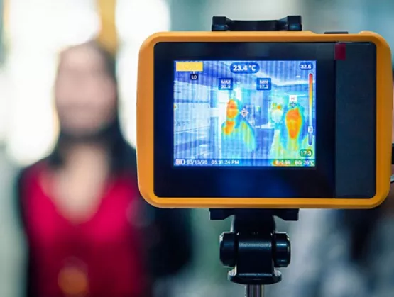
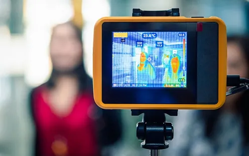
(The following is an excerpt of an article published by i-Micronews.)We are today entering a new era when sanitary checks will be regularly required to travel, do shopping, or have a social and cultural life. In this article and the related new Yole Développement (Yole) report, Thermal Imagers and Detectors 2020 – COVID-19 Outbreak Impact – Preliminary Report, we analyze how the COVID-19 outbreak could affect the thermal technology market and industrial landscape.To resume normal air traffic, air passenger screening to detect travelers with signs or symptoms of infectious disease will require new modalities. Thermal imagers could be used as a fast primary testing solution. This won’t be the first time actually. In the previous SARS, H1N1 and Ebola epidemics thermal cameras were used in some airports to screen travelers for fever. Of course, the size of the previous epidemics was not big enough to give this technology much attention. The way forward would be a triage process. Thermal imagers based on microbolometer technology can be installed at airports. If a fever is detected, then the traveler could be taken aside to get further tested with a more accurate handheld contactless thermometer. If the fever is proven, then they can be isolated for further examination, either a history check, and/or a diagnostics test, provided that it gives results in a reasonable amount of time.Airports are not the only places where thermal imagers can be the new norm. In April 2020, more than 50 Amazon warehouses had cases of COVID-19. Typically, workers were having their temperatures checked by handheld thermometers at the entrance. Amazon installed thermal cameras at some of their sites, which allows for faster screening. If needed, a secondary, forehead temperature check is performed if the employee is flagged from the camera, according to Reuters. Other companies that have explored using the thermal camera technology include Tyson Foods Inc and Intel Corp. Even some schools in China have started using them. This is an example of how businesses and infrastructure are turning to methods for containing the spread of virus by using technologies that previously went unnoticed by the general public.More businesses can adopt thermal cameras. In all countries, between 5% and 10% of enterprises employ more than 50 people, according to the OECD. To return to work, they could use thermal cameras to monitor body temperatures of employees as well. Here we are talking about cameras in the order of hundreds of thousands units.But this might not be enough. Everyone will probably want to have the ability to check their body temperature at any time. We have here a big market opportunity for integration of thermal imaging into smartphones or wearables. This integration has been in process for years. And it has long been perceived as the next sensor to be integrated in a mobile phone after pressure, inertial MEMS, or CMOS imagers. However, when 3D sensing technology was launched by Apple in 2017, all smartphone manufacturers focused their effort on this application, and were not interested in thermal imaging. Nowadays, because of the COVID-19 pandemic, people are much more sensitive to checking their own temperature and those of people around them, usually several times per day. Integration of a contactless thermometer could make sense. So there could be a revival of the use case of thermal imaging capability or temperature measurement in a smartphone or a wearable in the future.Click here to read the full article in i-Micronews.Eric Mounier Ph.D. is Fellow Analyst at Yole Développement (Yole). Dimitrios Damianos, Ph.D. is a Technology and Market Analyst at Yole Développement (Yole) working within the Photonics, Sensing Display division.Yole Développement is a member of SEMI and the MEMS Sensors Industry Group (MSIG), a SEMI Strategic Association Partner.
Read More
As government and business leaders start to talk about “returning to normal,” and looking to thermal cameras to help, questions remain about how and whether the latest technology can help prevent the spread of COVID-19.Across industries, everyone is looking for the right tools to help detect, slow and eventually stop SARS-CoV-2, the virus that causes COVID-19. By now we’ve all come to recognize that resuming operations in any way will require demonstrating measures to protect the health and wellbeing of people in a variety of situations, including travel and work.One proposed solution is thermal scanners. Unlike most medical imaging approaches, infrared (IR) thermography doesn’t require irradiation or expensive equipment, and presents no health hazard. Infrared radiation emitted from our skin can be detected and used along with information about the ambient environment to estimate core body temperature — which may indicate someone is running a fever, a common early symptom of COVID-19. While thermal cameras can’t detect a virus or a specific infection, they can help by quickly narrowing down a large pool of possibly infected individuals. And today, this represents the only viable non-contact mass screening approach for fever. The accuracy of the infrared system can, however, be affected by human, environmental and equipment variables. Understanding this multitude of variables — including the ways in which the science, technology and applications themselves interact — will help both users and system makers deliver the best results.Consideration #1: Think about the methodThermal detection has been used for fever detection for 20 years now. While older thermometers and thermal cameras, including the type used to detect a different coronavirus, severe acute respiratory syndrome (SARS), had their weaknesses, newer generations deliver significant performance improvements. More intelligent systems now offer features such as real-time calibration to ambient temperature with sub-degree °C accuracy, providing more accurate readings far more quickly than older generations.Newer camera systems are also more user-friendly and more reliable, featuring automated target recognition, improved resolution, pairing with a visible-light camera, automated alarms for febrile cases, and clearer outlining of hot spots. This higher degree of granularity improves insight, allowing for a more efficient and faster screening process, and provides on-site health professionals with necessary information to take additional steps when required. Advanced image processing features in new radiometric thermal cameras. Consideration #2: Know your baselinesBecause the environment can influence temperature measurements, some system makers have devised different ways to establish functional baselines. An early approach, recording a population baseline at each site on each day, proved too time- and resource-intensive. A newer approach, using a reference temperature source, or black body, offers evolutionary improvement. Designed to maintain itself at a specific temperature, the black body device allows the thermal camera system to automatically calibrate. Even better is a radiometric camera, which can intepret the intensity of an infrared signal reaching the camera. This requires more rigorous design and testing by the manufacturer, but it delivers much more precise measurements.Diagram of a fever detection system with black body emitter Consideration #3: Looking in the right place While thermal cameras can only detect surface temperatures, different parts of the human body more closely correlate with body temperature. Based on recent scientific research, the most reliable spot in the human face is the canthus, the small corners over the tear duct of your eye where the upper and lower eyelids meet. This kind of precise targeting requires accurate pixel calibration capabilities. The best surface target for estimating core body temperature: the canthus at the inner eye Consideration #4: Checking your performance Operating an IR fever screening system in the lab is one thing, but out in the field, the situation becomes more complex. Users need a camera system that is reliable and stable when it comes to critical performance factors like resolution, sensitivity and frame rate. Understanding the performance considerations when imaging a subject at a distance, for example, and realizing the minimum number of pixels required to get an accurate measurement are both essential in staging a fully optimal fever-detection platform.Consideration #5: Finding your way in the “wild west” of thermal imaging in early 2020People from the many industries that have been devastated by this pandemic – including travel, sports, manufacturing, food and hospitality, and entertainment — are looking for ways to reopen businesses safely while reducing the probability of a second wave of COVID-19. Deploying technology such as IR fever screening systems as part of a range of preventative measures will hopefully support that effort.As is the case with any promising emergent technology, there is a fair degree of chaos around the nuanced considerations of system design and performance. What standards apply to IR fever-screening devices? Which are being enforced? Who makes them? Will they work? IR camera manufacturers such as Teledyne DALSA and the expert system integrators we work with can play an important role in helping manufacturers and integrators to navigate this chaos, enabling us to work together to potentially save lives.For an even more in-depth look at this topic, visit this page, download our whitepaper Thermal Imaging Technology for Fever Screening, or browse.Jean Brunelle, product manager for infrared imaging, is a technical leader in sensor integration at Teledyne DALSA. He works on developing new image correction and calibration algorithms as well as qualification and production tests for the company’s visible and LWIR lines of digital cameras. Having earned a bachelor’s degree in engineering physics and a masters in surface chemistry, he has a passion for all things sensors, from how they work to how they are fabricated and used. His focus for the past few years has been on micro-bolometer-based LWIR cameras. Most recently, he was involved in the development and testing of Teledyne’s very own WLP micro bolometer and its integration into a thermal camera.Teledyne DALSA is a member of MEMS Sensors Industry Group (MSIG), a SEMI technology community that enables the MEMS and sensor industry to address common challenges, innovate and accelerate business results.
Read More
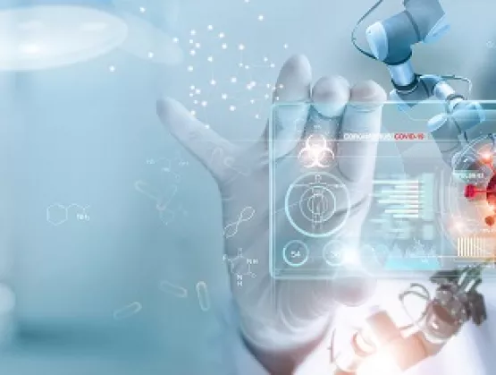
Thanks to developments in science and technology, artificial intelligence (AI), cloud computing, big data and other technologies have been used to establish smart healthcare systems that helps societies respond more effectively to disease outbreaks. The spread of novel coronavirus starting in late 2019 has revealed how not only traditional medicine but also Smart MedTech applications can be instrumental on the anti-epidemic front lines.To give updates on the development of Smart MedTech and how it shines during the fight against COVID-19, SEMI invited Dr. Pei-Yuan Lee, Honorary Superintendent of Show Chwan Memorial Hospital, to share with MSIG (MEMS Sensors Industry Group) and Flex-Tech members how the international community and Taiwan are bringing their best in Smart MedTech to the table and how their collective efforts are helping tackle COVID-19 challenges.Taiwan’s COVID-19 rapid screening reagents and antibody testing help curb coronavirus transmissions Taiwan’s medical community has demonstrated its prowess in responding to the COVID-19 outbreak. Using its nucleic acid extraction reagent, Taiwan Advanced Nanotech Inc. tested 128 specimens from passengers aboard the SuperStar Aquarius cruise ship in only eight hours in early February. Taiwan’s leading research institute Academia Sinica successfully synthesized the first group of monoclonal antibodies capable of recognizing the new coronavirus protein on March 8, enabling testing to be completed in 15 minutes. The College of Medicine of National Taiwan University announced on March 27 that its 30-second screening device had helped identify asymptomatic carriers. The devices detect COVID-19 in people with no symptoms if they have pulmonary infiltration and edema. It took only 14 days for Academia Sinica to successfully synthesized the first group of monoclonal antibodies capable of recognizing the new coronavirus protein. On April 22, three biomedical companies in Taiwan launched a COVID-19 test that produces results from samples of patient mucus in less than 10 minutes to greatly enhance testing speed. Once the test method is approved by the Taiwan government, it will take Taiwan’s medical strategy against COVID-19 to the next level.Artificial Intelligence: the key to upgrading traditional healthcare practicesAI is a key enabler of the transition from traditional medical practice to Smart MedTech. To help fight the COVID-19 outbreak, a National Cheng Kung University medical team developed a 30-minute coronavirus testing procedure that uses AI to read pulmonary X-ray images and automate medical records. Taiwan AI Labs leveraged AI to simulate how drug molecules combine with viruses to reduce research time by three to four years. AI ​​diagnostic technology from the Alibaba DAMO Academy (Academy for Discovery, Adventure, Momentum and Outlook) and Alibaba Cloud interprets CT images of COVID-19 patients with 96 percent accuracy in 20 seconds. AI-powered algorithms improve diagnostic test accuracy, allowing clinicians to quickly analyze scans of pulmonary lesions and quantify the severity of lung damage.Startups have also joined the fight against COVID-19. Taiwan's Internet of Things (IoT) startup iWEECARE invented the world's smallest smart thermometer patch. Heroic-Faith Medical Science launched a device that uses IoT and AI to monitor lung sounds. With Smart MedTech expected to be fertile ground for future venture investments, enterprises must find their niches in establishing new technologies in a much more systemic way. Taiwan startup Health-Faith Medical Science developed a respiratory diagnostics device that uses IoT and AI technology to monitor chest sounds in real time. Anti-epidemic technology to help fulfill smart medtech vision Many AI and big data technologies previously deployed in hospitals and healthcare systems are helping regions around the world speed their pandemic response. The United States and China have started to develop facial mask recognition systems powered by AI, while a team in the Department of Bioinformatics and Medical Engineering at Asia University has devised a facial recognition system combining IoT and AI technology with infrared thermal imaging cameras. At Johns Hopkins University, the Center for Systems Science and Engineering is using AI to create big data models that track global cases, people and traffic flow, and other variables for real-time data analysis that enables epidemiologists to more accurately predict COVID-19 transmission paths. Graphen, Inc., a New York-based provider of next-generation AI platforms, launched the world's first AI COVID-19 genetic evolutionary path analysis systems to gauge the virus’s transmission route and accelerate pandemic response. Both the United States and China are also using robots and drones to improve epidemic research and patient treatment. For the first confirmed case in the United States, robots were used to assist with medical care. In China, robots facilitate deliveries of disinfectants to makeshift hospitals built to expand the nation’s capacity to treat COVID-19 patients. While Taiwan’s robots are traditionally used for hospitality, transportation and disinfection purposes, future robotics research and development will focus more on medical applications that shift more work from medical staff to technology. With abundant technological resources and expertise, Taiwan can join hands with the rest of the world to combat the COVID-19 pandemic. Emerging technologies are pointing the way toward a new paradigm for healthcare community. Biotech, artificial intelligence, and robotics have given rise to new applications that increase virus screening accuracy and efficiency. This growing wave of technological defenses against the pandemic will become a long-term force for stability and strength in healthcare systems across the world.To get involved in SEMI Taiwan Smart MedTech Community, please contact Helen Chen, Outreach Manager, at [email protected] Huang and Winnie Chang are marketing and public relations specialists at SEMI Taiwan.
Read More
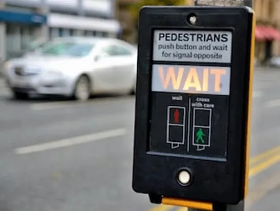
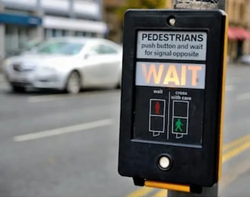
The COVID-19 pandemic (caused by SARS-CoV-2) has disrupted lives around the world more than any other catastrophic event in living memory. Those of us fortunate enough to work from home are cheering on the people who care for our health, transport our packages, work in grocery stores and pharmacies, clean public streets and buildings, and keep utilities up and running — as well as everyone else on the front lines of battling this pandemic. Working from home also gives us time to reflect and ask: How does the world return to normal and how can we help?Crises like the COVID-19 pandemic accelerate social and technology trends because the need for new solutions grows urgent. Looking at epidemiological models can reduce complex disease progression to a series of simple numbers, the most important of which is R nought (R0) value. R0 is simply how many other people a sick person infects. If each sick person infects less than one person, R0 1, the spread of disease will end. But if each sick person infects more than one other person, the disease spreads and may become a pandemic. According to the journal Emerging Infections Diseases, SARS-CoV-2 has an R0 of 5.7, making it far more infectious than the influenza pandemic of 1918.Given the severity of the current pandemic, society has taken huge efforts to reduce R0: mask-wearing, social distancing, avoiding face touching, frequent handwashing and quarantines are all ways to reduce R0.Scientists and engineers are working hard to develop new solutions and evaluate existing technologies that could have a big impact on R0. One of these is the mass deployment of touchless technologies. We’re now aware that every time we touch a surface, we potentially spread disease. I have personally started using touchless Apple Pay at retail checkouts whenever possible and even seek out and remember which stores have enabled Apple Pay. Each time I need to touch an elevator button, security keypad or walk signal button at an intersection, I contort my arms to touch them with an elbow.Since I’m in the electronics industry, I find myself considering which devices have the greatest potential for reducing the number of touchpoints in our daily lives. Motion and ultrasound sensors are definitely promising, but the mainstream adoption of the voice interface makes it the most interesting and scalable touchless technology.New voice technologies are more reliable and secure than ever. The success of cloud-based voice assistants such as Amazon Alexa, Apple Siri and Ok Google has familiarized consumers with the ease and convenience of voice, but these high-powered AI assistants generally require high power and a reliable internet connection. The next wave of voice technology will be much lower in power, fast, private and require no internet connection. This edge-powered voice interface will not play music or tell you the weather, but it will perform many other useful and simple functions, such as operating an elevator, opening a door or changing the volume on your TV. One great example of this local voice command is the Simple Human trash can that can open and close in response to your voice. Opening and closing a garbage may be simple, but a voice-activated model enhances convenience and safety with total privacy.The requirements for deploying voice technology to support more touchless applications include: Low power — to run for months or years between battery changes Robust and reliable— to last over a decade indoors or out Locally processed data — to ensure security and privacy without an internet connection Consumer adoption of touchless and voice technologies has been growing for years, but the COVID-19 crisis highlights the critical benefit of these technologies in reducing the spread of disease. Making high touchpoints voice-powered would eliminate a disease vector and reduce R0 during pandemics as well as during normal cold and flu seasons. Any technology that helps reduce R0 should be deployed as quickly as possible to give us one more way to thwart the virus that is changing life as we know it.As the only supplier of piezoelectric MEMS microphones – which are natively immune to environmental contaminants such as water, humidity, salt, dust, dirt and oil — Vesper is uniquely able to provide outdoor-hardened microphones that are durable enough to support voice-interfaces in hot, wet, dusty or dirty conditions. In fact, we’ve earned the highest waterproof rating for any MEMS microphone – IP57 – which makes me hope that one day soon I’ll use just my voice to tell a crosswalk signal that I need to cross the street.Vesper has also developed a proprietary technology called ZeroPower Listening, which makes it possible to embed always-listening voice interfaces in battery-powered devices with battery life measured in months or years. And that’s just the beginning of how we’ll use voice interfaces in high-touch applications. From voice-controlled parking kiosks and elevator buttons to the treadmill at the gym, the less we touch hard surfaces, the safer we’ll be from picking up SARS-CoV-2, influenza viruses or other pathogens as we go about our daily lives.Learn how Vesper’s low-power and rugged MEMS microphone technology can help designers create seamless voice interfaces for a wide range of indoor and outdoor applications at Smart Home, Smart Office, IoT and Automotive/Industrial.Matt Crowley is CEO of Vesper Technologies, developer of the world’s first piezoelectric MEMS microphone. With five rapid product rollouts in just five years and tens of millions of units shipping to tier one clients across the globe, Matt has grown Vesper from a research-oriented startup to a bonafide commercial business.Under his leadership, Vesper has earned an impressive collection of awards including a 2019 Best of Sensors Award, Innovation Award nods at CES 2018 and 2019, and two Annual Creativity in Electronics (ACE) Awards.Before Vesper, Matt held leadership positions at piezoelectric MEMS pioneer Sand 9, the Boston University Office of Technology Development, and Mars Co strategy consulting, where he advised Fortune 500 companies on operational and strategic issues.Matt received an interdisciplinary degree in Physics and the Philosophy of Science from Princeton University. He is proficient in Japanese, having lived in Japan.Vesper is a member of MEMS Sensors Industry Group (MSIG), a SEMI technology community, that enables the MEMS and sensor industry to address common challenges, innovate and accelerate business results.
Read More
On Saturday, March, 21, 2020 the U.S. Food and Drug Administration (FDA) gave emergency authorization to Cepheid, a California company, to sell a new test for rapid detection of the pandemic coronavirus SARS-CoV-2, which causes COVID-19. Cepheid’s Xpert® Xpress SARS-CoV-2 test gives healthcare workers results in just 45 minutes, with less than a minute of hands-on time for sample preparation.Cepheid, founded by Kurt Petersen, M. Allen Northrup and five others in 1996, is well known in the MEMS community for commercializing microfluidic chip-based polymerase chain reaction (PCR) analysis machines. This is not the first time Cepheid has responded quickly to a biological threat; after the 2001 terrorist attacks in the USA, Cepheid was the first to provide rapid anthrax detection capabilities to the U.S. Postal Service, and it still does today.At the heart of all COVID-19 test protocols (see the WHO protocol and U.S. CDC protocol) is the real-time reverse transcription polymerase chain reaction (RT-PCR) analysis technique. In a very simplified description, PCR uses thermal cycling to amplify the DNA present in a patient’s swab sample, and then using fluorescence optical detection, searches for the virus’s specific DNA. The test requires knowing the virus’s genome in the first place; the crucial work to sequence the full genome of SARS-CoV-2 was first published by Chinese scientists for public use on January 10, 2020.While traditional PCR machines take many hours to thermal cycle and reach a result, MEMS-based PCR systems can work much faster. Featuring scale heaters and reaction chambers that have a tiny thermal mass, they create a significantly faster heat-cool cycle, enabling a rapid result in minutes.The first MEMS silicon PCR chip, developed by Northrup et. al. at Lawrence Livermore National Laboratory and licensed to Cepheid (left) and the Cepheid test cartridge today (right). (Source: Northrup MA, Ching MT, White RM, Watson RT, “DNA amplification in a microfabricated reaction chamber,” Transducers 1993, Yokohama, Japan. pp. 924–926.) Research on MEMS-based PCR systems has continued steadily since the early 1990s. Today, researchers have been focusing on developing highly integrated, low-cost systems specifically for point-of-care use. One example of recent research: a team at Korea’s ETRI and Genesystem have developed a prototype low-cost, handheld PCR system having a polyimide chamber and microheater and an integrated CMOS detector for optical readout of results (figure below). Cross-section schematic of the chamber, heating module and integrated optical detector in a portable PCR prototype (left) and integrated test cartridge (right). (Source: DS Lee, OR Choi, and YJ Seo, “A Handheld and Battery-Powered Realtime Microfluidic PCR Amplification Device,” Transducers 2019, Berlin, Germany pp. 1063-1065.) Korea’s quick recruitment of its biotech companies and creation of novel drive-through testing sites helped it to successfully pinpoint its COVID-19 outbreak and to implement control measures. Let’s hope the Cepheid test can be similarly effective.Based on successive epidemics of SARS, MERS and now COVID-19, rapid PCR test machines, enabled by MEMS technology, are becoming essential medical tools in the fight against viral outbreaks. As continued development lowers the cost of such critical equipment, let’s hope we may soon have a PCR machine in every doctor’s office.Alissa M. Fitzgerald, Ph.D., founded A.M. Fitzgerald Associates, LLC (“AMFitzgerald”), a MEMS and sensors solutions company based in Burlingame, CA, in 2003. She has over 25 years of engineering experience in MEMS design, fabrication and product development.Prior to founding AMFitzgerald, Fitzgerald worked at the Jet Propulsion Laboratory, Orbital Sciences Corporation, Sigpro, and Sensant Corporation, now part of Siemens. She received her bachelor’s and master’s degrees from MIT and her doctorate from Stanford University, in Aeronautics and Astronautics. Fitzgerald has numerous journal publications and holds eight patents. She served on the Governing Council of MEMS Industry Group from 2008-2014 and was inducted into the MIG Hall of Fame in 2013. Fitzgerald serves on the Board of Directors of both Rigetti Computing and the Transducer Research Foundation.AMFitzgerald is a longtime member of MEMS Sensors Industry Group (MSIG), a SEMI Strategic Association Partner. For more information on AMFitzgerald, please visit: https://www.amfitzgerald.com.Interested in learning more about this topic? Read Alissa M. Fitzgerald and Farzad Khademolhosseini’s article in EE Times, MEMS in the Fight Against Covid-19.
Read More
The seemingly simple act of commanding consumer devices by voice is a choice that nearly 118 million Americans now make every day, according to a recent report from eMarketer, the digital marketing research firm.While the voice interface is convenient for users, its implementation comes at the potential loss of individual privacy. The reason? Always-on, always-connected voice-first devices such as Amazon Alexa and Google Home require a wall plug and an internet connection to powerful cloud processors, making it possible for cloud companies — however benignly — to collect data on personal habits, location and conversation that were never intended for sharing. Move processing to the edgeTo address concerns over user privacy, device designers are attempting to do more of the audio processing within the consumer device, rather than sending users’ voices into the cloud. Moving more processing to the edge is a trend across the Internet of Things (IoT) industry, and not just for voice data but for other types of sensitive or proprietary data as well.Yet designers have realized limited success because the conventional approach to always-listening edge processing is notoriously inefficient: It digitizes and processes 100% of incoming sound data even though up to 90% of the data is irrelevant noise. This digitize-first approach wastes vast amounts of system power digitizing and analyzing the audio signal as it searches for a wake word when there isn’t even speech present, making it impractical for use in small, battery-operated devices.Workarounds don’t workTackling this power issue is critical to keeping private data secure. Unfortunately, it’s also exceptionally difficult. Design engineers have tried workarounds to decrease power consumption in an always-listening system, including duty cycling and reducing the power of each individual component in the audio signal chain that handles the data. The reality is that these kinds of approaches don’t address the root cause of the problem: too much data.To truly tackle the problem, we need to change our approach to a system solution, not a component solution. By moving to a more efficient edge architecture that intelligently minimizes the amount of data that moves through the system, we can focus the system’s energy resources on analyzing voice and not on searching for a wake word in irrelevant noise. Analyze, THEN digitize It’s time to move away from the digitize-first approach that has dominated voice wake-up device architecture since the invention of voice-first applications.Inspired by the way the human brain efficiently filters incoming information, differentiating, for example, a dog bark from a baby’s cry, an ultra-low-power analog machine learning technology is changing this paradigm. For the first time, device designers can use low-power analog machine learning to detect which data are important for further processing and analysis prior to data digitization.Leveraging an analyze-first architecture, a new analog neuromorphic semiconductor platform allows the higher-power-processing components in the system to stay asleep until voice has actually been detected, and only then does it wake them to listen for a possible wake word.Delivering a post-microphone audio chain that draws as little as 25µA of current when always-listening and collecting preroll data, this analyze-first architecture allows designers to extend battery lifetime significantly. That’s the difference between smart earbuds that run for weeks instead of hours or a battery-powered smart speaker that runs for months instead of weeks.More importantly, it’s the difference between the current always-listening devices that indiscriminately record and send all sound data to the cloud, and one that has the localized intelligence to select and send only the relevant data, reducing the user’s vulnerability to the loss of private data.Balance convenience with privacyThe trade-off between making our lives easier and keeping our personal information private is a choice that we are asked to make throughout our day in a hundred different ways. Bringing more audio processing capability to the mobile device without draining the battery is the first step toward delivering more secure voice-first solutions. But to succeed in this effort, we must shift to a bio-inspired architecture that determines which data are important and requires further processing at the earliest point in the signal chain. Once we move to the analyze-first approach, only a small fraction of the tens of zettabytes of data collected by the forthcoming generation of always-on IoT devices will require further processing in the device and in the cloud.A better balance between cloud and edge processing is a better balance between convenience and privacy, and that’s a win for everyone.About the AuthorTom Doyle is CEO and founder of Aspinity. He brings over 30 years of experience in operational excellence and executive leadership in analog and mixed-signal semiconductor technology to Aspinity. Prior to Aspinity, Tom was group director of Cadence Design Systems’ analog and mixed-signal IC business unit, where he managed the deployment of the company’s technology to the world’s foremost semiconductor companies. Previously, Tom was founder and president of the analog/mixed-signal software firm, Paragon IC solutions, where he was responsible for all operational facets of the company including sales and marketing, global partners/distributors, and engineering teams in the US and Asia. Tom holds a B.S. in Electrical Engineering from West Virginia University and an MBA from California State University, Long Beach. For more information, please visit https://www.aspinity.com/Technology.Aspinity is a member of MEMS Sensors Industry Group (MSIG), a SEMI technology community, that enables the MEMS and sensor industry to address common challenges, innovate and accelerate business results.
Read More
As the body’s largest organ, skin is responsible for the transduction of a vast amount of information. This conformable, stretchable, self-healable and biodegradable material simultaneously collects signals from external stimuli, which translates into information such as pressure, pain and temperature. The development of electronic materials, inspired by the complexity of this organ, offers a tremendous unrealized materials’ challenge. Fortunately, the advent of organic-based electronic materials may offer a solution to this longstanding problem.Zhenan Bao, K.K. Lee Professor of Chemical Engineering, Stanford University, is one of the world’s leading researchers working on the design of organic electronic materials that mimic skin functions. SEMI’s Maria Vetrano interviewed professor Bao to preview her February 25 keynote, Skin-Inspired Electronics, at FLEX|MEMS Sensors Technical Congress (MSTC) 2020, February 24-27, 2020, at the DoubleTree by Hilton in San Jose, California.Join us at FLEX|MSTC to meet Professor Bao and other industry influencers furthering innovation in flexible hybrid electronics (FHE) and MEMS sensors. Register now to connect with her at FLEX|MSTC or visit her on LinkedIn.SEMI: Your pioneering work on the use of electronic materials to construct second skin is a major step forward in human-machine interfaces. Could you please describe second skin?Bao: Second skin is a new electronic-device platform encompassing electronic devices that have skin-like properties such as stretchability, self‐healing ability, biocompatibility and biodegradability. In essence, the second skin is an electronic system of fully integrated multifunctional components operating on the surface of or inside the body to enable smart healthcare for disease prevention and treatment and to enhance the functional capabilities of natural skin. The second skin could also serve as a module to connect our human body to the Internet, thereby allowing human integration with the Internet of Things (IoT) for next‐generation wireless communications. In this way, we can view the second skin as an artificial body part that can be used to improve our everyday lives.SEMI: How might second skin operate in the human body?Bao: It has many potential uses. It could be a prosthesis for people who have lost their sense of touch. It could be used to repair damaged skin as well as to provide enhanced functionality that’s not possible with biological human skin. It could, for example, connect us with our external environment, with other people, even with our cars.I can also envision second skin as an implantable device for both neurostimulation and for early detection of disease. Schematic illustration of structure of second skin composed of functional devices: sensor, integrated circuit, display and power supply. Source: Stanford University SEMI: How did you get started in this research? Bao: Sixteen years ago when I started at Stanford, I learned of a colleague in mechanical engineering who was working on robotic cockroaches. That’s when I understood the need for sensor functions in robotics.I considered the large number of people with prosthetics who do not have a sense of touch. With this audience in mind, I started by designing a simple flexible electronic device that could take the shape of skin, even conforming to a robot hand, thereby approximating the natural sense of human touch.Once we developed the first sensor, and realized that its touch sensitivity could eclipse that of human touch, I asked myself: what can we learn from second skin – in addition to its sensing functionality?Skin is not just flexible; it is biodegradable and stretchable. So we started to dream. We began by developing electronic materials, either conductors or semiconductors. We added new functionality, such as self-healing properties, biodegradability and stretchability. That opened the way to new materials’ development.SEMI: What discoveries have you made in new materials?Bao: Over the past decade, we’ve developed skin-like materials with electronic properties that are on par with the best conducting and semiconducting polymers. Some of our skin-like semiconducting polymers can perform even better than amorphous silicon. That means with suitable processing methods, we can make stretchable ICs, initially with tens of transistors that can perform analog or digital functions, and in a later stage, stretchable displays driven by active matrix arrays.SEMI: What would it take to put these materials into production?Bao: We need to develop methods to pattern the skin-like electronic materials into fine features. We have been leveraging similar processes used for flexible circuit boards. Some research groups are developing roll-to-roll fabrication and printing methods.SEMI: Which technologies/applications are you commercializing?Bao: C3Nano is a Bao Research Group spin-off startup that is commercializing nanomaterials that are promising for bendable and foldable electronics.Another spin-off that is licensing our technology, PyrAmes, is developing a continuously non-invasive blood-pressure monitor. It’s not a cuff so the patient doesn’t have to remember to put it on.In the shorter term, we’re looking at putting artificial skin on prosthetic limbs and robotic hands. Further down the road, we could put skin on wounded regions of the body, forging connections to nerves that would support realistic sensation.To realize these applications, we’ll need to conduct further R D on materials and applications. The manufacturing of these devices still needs much more development.Fortunately, we’re part of a fertile development ecosystem at Stanford. I started the Stanford Wearable Electronics Initiative (eWEAR) to forge collaborations across Stanford campus as well as with industry.SEMI: What would you like FLEX|MSTC attendees to take away from your presentation?Bao: I’d like them to realize that the future of electronics is changing. I imagine a future in which the functions of a smartphone will disappear into what we wear, what we attach to our skin and what we implant inside our body. I believe that skin-like electronics will help to facilitate this future, allowing us to connect with each other and our surroundings in ways that feel natural, yet that also enhance our quality of life. Zhenan Bao is K.K. Lee Professor of Chemical Engineering with courtesy appointments in Chemistry and Material Science and Engineering at Stanford University. She founded the Stanford Wearable Electronics Initiate (eWEAR) and serves as the faculty director. Prior to joining Stanford in 2004, she was a Distinguished Member of Technical Staff at Bell Labs, Lucent Technologies from 1995 to 2004.Bao has over 500 refereed publications and over 65 U.S. patents with a Google Scholar H-Index 155. In her recent work, she has developed skin-inspired organic electronic materials, which have resulted in unprecedented performance or functions in medical devices, energy storage and environmental applications. She has pioneered several important design concepts for organic electronic materials. Her work has enabled flexible electronic circuits and displays.For more information on professor Bao’s research, visit Bao Research Group. FLEX|MSTC is organized MEMS Sensors Industry Group (MSIG) and FlexTech, SEMI technology communities focused on the growth of MEMS sensors and the flexible electronics supply chain, respectively. Maria Vetrano is a public relations consultant at SEMI.
Read More
MEMS technology has changed human interaction with electronic devices. Introduced in the 1990s, the first mass-market MEMS devices were used for inkjet printheads and automotive airbag crash sensors. Today, MEMS are ubiquitous, with billions of the tiny devices adding intelligence and interactivity to smartphones, smart speakers, wearables, automobiles, biomedical devices, remote monitoring and event detection systems, and countless other applications. Integrating MEMS with Flexible Hybrid Electronics (FHE) is an important step in the evolution of this miniaturized intelligent sensing technology, paving the way for its use in new classes of flexible, conformal devices.The integration of the two technologies promises to breed new applications in small form factors but also presents challenges inherent to FHE design and fabrication processes. SEMI’s Nishita Rao caught up with Nathan Pretorius, prototyping and automation engineer, NextFlex, to discuss MEMS-FHE device integration challenges and opportunities ahead of his February 26 presentation, Integrating MEMS Devices in FHE, at FLEX|MEMS Sensors Technical Congress (MSTC) 2020, February 24-27, 2020, at the DoubleTree by Hilton in San Jose, California.Join us at FLEX|MSTC to meet Nathan and other industry influencers advancing innovation in FHE and MEMS sensors. Register now to connect with him at FLEX|MSTC or visit him on LinkedIn.SEMI: Why is integrating MEMS devices into FHE systems important? What new use cases might it enable?Pretorius: The main value proposition of integrating MEMS devices into FHE is that it allows MEMS devices to exist in a different form factor than was possible previously, giving us high-quality MEMS sensors on the flexible and conformable platform of FHE.Ease of application, flexibility, lower cost and rapid iteration on a design are just some of the benefits of FHE devices. And because there are few robust FHE sensors that overlap with MEMS’ capabilities, when you combine the two, you get a lot of compelling uses. That’s why NextFlex is working with agencies and companies to evaluate MEMS’ integration, including using bare MEMS die with microfluidics and promoting new ways of attaching and packaging MEMS die for use with FHE. SEMI: Why is FHE an ideal platform for integrating various types of sensors?Pretorius: MEMS integrated with FHE devices are ideal for rapid design and deployment of data-gathering sensor nodes — which we can iterate for specific applications. A few examples include on-body health monitoring devices for bio-fluids analysis, medical pressure sensors for monitoring blood pressure, and peel-and-stick sensors nodes for infrastructure monitoring. In terms of design and production, FHE devices support rapid prototyping, allowing for instantaneous design-iteration cycles. This speeds design-to-production over traditional rigid PCBs and copper flex because the feedback cycle time between design, manufacturing and testing is shorter, accelerating time to market. What’s exciting about FHE technology is that a variety of sensors or components, including MEMS, can be designed into the base system to easily customize it for a specific application. In addition, our experience shows that when compared to a traditional rigid PCB, an FHE board reduces manufacturing steps and device weight by two-thirds and, perhaps most importantly, converts the device to a thin, conformal shape that makes possible products in new form factors. SEMI: What are the primary challenges to integrating MEMS with FHE? What is NextFlex doing to help device manufacturers address these challenges? Pretorius: There are a few challenges, some of which are device-specific. Most recently, I’ve been focusing on inertial and timing devices, including accelerometers, gyroscopes and resonators. There are a few technical challenges involved in the process of getting the devices from the wafer to an FHE substrate. The wafer processing is very important, especially the dicing and thinning steps. After thinning and dicing, the die is placed onto the FHE substrate. The stresses caused by bonding to the substrate have to be understood and characterized. After placing the die, you then have a calibration step, which is normally performed after the device is packaged. With a MEMS die placed onto directly onto an FHE substrate, calibration then must be done.Finally, the device encapsulation is important, since on an FHE substrate the hard-to-soft material transition is very important to mitigate stresses to rigid component interfaces. We have also been looking at how to work with devices that have damping vents. Flexible encapsulants are inherently more permeable to gases and water vapor than hard encapsulants, so studying the encapsulation of MEMS devices on FHE is another area of interest. NextFlex has been working in a supporting role to evaluate best design practices and best attach and integration methods. In addition to our ongoing collaborative programs, NextFlex is developing the FHE manufacturing ecosystem to include system and component manufacturers and designers, product developers, and materials and equipment providers.SEMI: How do we facilitate closer collaboration between the FHE manufacturing ecosystem and MEMS suppliers such as MEMS device manufacturers, product developers, and materials and equipment providers?Pretorius: It’s important to include manufacturers early in the design process so we can identify challenges up front. That’s why NextFlex spearheads technology road-mapping efforts that include representatives from across the manufacturing ecosystem. We use the roadmaps to prioritize challenges that we can address effectively through collaboration, focusing the industry on solving problems through Project Calls that reveal integration challenges and results from real devices and that tell us how the materials and equipment actually perform with a real device.NextFlex keeps the information flowing, holding quarterly project update webinars to share results. As current devices are optimized for the process in which they will be used, we learn a lot from the project performers who make FHE system demonstrators — and we share that information with the member community. SEMI: Can you point to an example of a successful MEMS-FHE device integration?Pretorius: MEMS-FHE integration is still in the early stages, but we are working on several projects including a DARPA Seedling project for which we have integrated MEMS sensors into FHE systems for testing and evaluation. We plan to continue this work by integrating MEMS and FHE devices using methods that support mass production.SEMI: What would you like FLEX|MSTC attendees to take away from your presentation?Pretorius: We would like to see the FHE community work more closely with MEMS device manufacturers. For example, NextFlex often works with manufacturers to gain access to bare die, which is still a significant hurdle in making devices.The best way to speed things along is to get involved. We encourage FLEX|MSTC attendees to join NextFlex. As a prototyping and automation engineer at NextFlex, Nathan Pretorius explores new print methods for prototyping and automation using novel materials and processes. Pretorius currently focuses on how best to apply software scripting and machine learning to streamline FHE processes. Prior to joining NextFlex, he researched the strengths of roll to roll and screen printing on printed electronics designs, including capacitive touch interfaces, FHE passive component design, and antennas. Nathan holds a Bachelor of Science degree in Graphic Communications from Clemson University. FLEX|MSTC is organized MEMS Sensors Industry Group (MSIG) and FlexTech, SEMI technology communities focused on the growth of MEMS sensors and the flexible electronics supply chain, respectively.Nishita Rao is marketing manager for technology communities at SEMI.
Read More