downloadGroupGroupnoun_press release_995423_000000 copyGroupnoun_Feed_96767_000000Group 19noun_pictures_1817522_000000Member company iconResource item iconStore item iconGroup 19Group 19noun_Photo_2085192_000000 Copynoun_presentation_2096081_000000Group 19Group Copy 7noun_webinar_692730_000000Path
Skip to main content
Default Banner Image

MEMS

MEMS and image sensors are shining stars in the chip industry as technology companies worldwide accelerate innovation in the fight against COVID-19. The tiny devices are behind advances in areas of electronics ranging from thermal imaging and faster point-of-care testing to microfluidics-based polymerase chain reaction (PCR) tools and techniques to detect SARS-CoV-2.SEMI recently spoke with Yole Développement analysts Dimitrios Damianos and Chenmeijing Liang about MEMS and imaging sensors market trends and how microelectronics-enhanced technologies are supporting the worldwide push to contain the spread of COVID-19.For additional insights on the technologies, join the SEMI MEMS Imaging Sensors Summit, held for the first time at SEMICON Europa, 12-13 November 2020 in Munich, Germany. Registration is open.SEMI: Despite the global pandemic, the MEMS and sensors market is still growing and is one of the healthiest industries, not only in Europe, but globally. What is driving this growth?Damianos: MEMS have been continuously evolving from the first sensors that were measuring pressure and acceleration to rotation sensing and visible light management followed by light sensing beyond visible and the expansion to ultrasound and multi-spectral. Now we are heading towards an era where we want to sense every aspect of our environment, with more processing and eventually analytics bringing more quality to the data.COVID-19 has impacted various global markets in very different ways. While automotive, mobility and civil aviation have suffered, the impact on telecommunications and medical has been positive. The effects on the consumer, mobile and industrial markets have been moderate. Moreover, COVID-19 is changing the perception of the current global supply chain in manufacturing, potentially leading to more localized value chains and further regionalization in order to minimize similar risks posed by the pandemic and the first lockdown.SEMI: Who are the main MEMS players based on your research? Damianos: For MEMS players, the picture in 2019 was not the same as 10 years ago, when Texas Instruments (TI) and Hewlett-Packard (HP) were leading the scene, with Bosch and ST Microelectronics following, all at comparable revenue levels. Now, Broadcom and Bosch lead with almost $1.4 billion in revenue each, and the rest of the MEMS key stakeholders compete in the $400 million to $600 million league. Microphone players profited from the voice interface adoption trend, while players active in MEMS for mobility and smartphones suffered slightly due to weak end-system demand.SEMI: What scenarios can we expect for each market with regard to the impact of COVID-19 on MEMS for 2020? Damianos: For 2020, at Yole Développement we expect the consumer market to contract slightly by 2.6%, with the automotive market to dip by 27.5%, and defense and aerospace by 20.5%. For the defense market, no major effect is expected, as all major programs still run for the year. The market may experience some slight delays in deliveries due to supply chain and logistics problems. However, sensors integrated in commercial/civil aerospace applications will suffer due to the general paralysis of the air travel industry. On the positive side, telecommunications could increase by 4.7%, medical applications by 10.6%, and industrial by 11.5%.Due to the global pandemic, some types of MEMS have spiked in demand this year. For example, demand for thermopiles and microbolometers used in temperature guns and thermal cameras has increased because of the need for contactless monitoring of people’s temperatures. Moreover, microfluidics for DNA sequencing and real-time polymerase chain reaction (PCR) diagnostic tests for detecting COVID-19 are gaining market relevance, with the latter serving as a premier method of detecting a bacteria or virus on the molecular level with high degrees of accuracy. Furthermore, pressure and flowmeters in ventilators will grow because of huge demand by hospital intensive care units (ICUs).SEMI: What growth trends do you predict for the long haul?Damianos: In the longer term, we expect global MEMS volumes to almost double, from 24.4 billion units in 2019 to 50.8 billion units in 2025, with a 13% CAGR during the same period. The global MEMS market could reach $17.7 billion in revenue by 2025.We see a trend to more wearable devices integrating a lot of sensors but also a move to a more consumer-oriented healthcare. Moreover, everything related to voice interfaces and voice/virtual-personal assistants (VPAs) will continue to see strong growth, increasing demand for MEMS mics with better quality and high-fidelity voice capture. MEMS devices are shifting to higher accuracy, ultra-low power, embedded intelligence and possibly some bio-compatibility for medical applications.MEMS players will try to escape the commoditization cycle and deliver more value by increasing the value of the data, either grouping many sensors to create sensor hubs or by adding processing, algorithms and software. Industry players are employing strategies such as adding extra processing close to the sensor (e.g. Knowles) or ameliorating the use cases of their applications of their clients (e.g. Bosch or ST). AI on the edge seems very alluring for extra value acquisition, with many startups already working on it. Some examples include always-on-sensing (Aspinity in collaboration with Infineon, Syntiant), echolocation (IMERAI) and predictive maintenance using inertial sensors (Cartesiam). This will be the next pit stop for MEMS technology for sure. SEMI: The CMOS Image Sensor (CIS) is a cornerstone technology in the development of devices powered by machine sensing and artificial intelligence (AI) for applications such as advanced driver assistance system (ADAS). CIS powers many of the ongoing revolutions in new technical products and use cases. What is the status of the image sensors industry? Liang: Last year was exceptional with a combination of high demand and high prices due to capacity limitations. Q4 2019 went way above the forecast, and, in the end, the CIS industry reached $19.3 billion for the full year. This year, we think it will return to normal, and, despite the pandemic impact, we expect significant growth in the range of 7% to 12%. Last year’s 25% year-over-year (YOY) growth was the highest we’ve seen over the past decade. Mobile still dominates the marketplace for CIS with 69% market share. Two markets, computing (8%) and consumer (5%), are adjacent to the mobile market but progressively losing ground due to the smartphone disruption.Security, at 6% market share, will probably be the second largest CIS market in the future. Although this is an area of excellence for the emerging Chinese players, unfortunately, they could be hit by the current trade war. The automotive market did very well from 2018 to 2019 because of the numerous applications recently developed for ADAS, viewing, and in-cabin applications. Lastly, the industrial camera applications benefited from large investments in automation, especially in the semiconductor and automotive industries, but here again many uncertainties remain as these markets will reshuffle in the post COVID-19 world. SEMI: Which CIS markets are most susceptible to seasonality and the impact of COVID-19?Liang: According to our quarterly CIS monitor, automotive and security were both negatively impacted by the pandemic beyond what we expected in terms of seasonality. For computing, the situation improved just prior the lockdown. Q1 got a positive impact with high sales results for laptops and tablets, but no significant impact was seen for security equipment. For automotive, the demand for cameras was very high in Q1, which is seasonally normal, despite the decrease of car shipments that followed later. The automotive CIS market in 2020 should remain relatively flat compared to 2019 due to the higher attachment rates of cameras despite the lower number of cars produced. Consumer and industrial segments dropped in Q1, which is typical early in the year.The next five years might be a bit slow, and although we forecast growth for the next year, in the future the market share will be lower in mobile. In fact, mobile CIS growth will fall below the CIS growth average, but we will see an increase of market share for the security, automotive and industrial segments. The CIS market could reach $28 billion in 2025.At first, COVID-19 had a limited impact on the production side, as factories in China are usually closed for the New Year holiday, when the pandemic started. While supply is currently recovering, we still consider the limited impact on demand. Smartphone production for 2020 will be down 6%, but camera shipments for mobile should increase about 10% this year. Another positive trend for the mobile market is optical fingerprint implementation. Currently, high-end Android phones use this kind of technology. For 2023, we estimate optical fingerprint technology revenue to be over $1 billion.The roadmap for the automotive market is driven by camera proliferation. We’ll see 10 cameras per car and more for some high-end vehicles. Increasing demand for safety and convenience will mean more cameras per car in the future. With a strong attachment rate, the market average in automotive is around 2.0 cameras per car nowadays, and we expect the market average to reach 3.5 cameras per car in 2025. In security, Charge Coupled Device (CCD)-based cameras are nearly out of the market, as CMOS-based IP cameras are most important now.SEMI: What are current key technology trends?Liang: 3D semiconductor technology is the hot topic. CIS wafer staking technology is indeed at the center of the CIS technology race. Future applications could be AI analytics or recently developed applications on new types of CIS. So far, we have seen the introduction of variants of the CIS pixel. Global shutter (GS) and indirect Time of Flight (iToF) were recently introduced, and now direct time-of-flight (dTOF) pixels are being used in high volume. 3D semiconductor technology is a bonanza for the industry, as it allows to pack more value in a single chip. While the surface of silicon is still increasing, additional silicon is added through stacking.With COVID-19 still a problem, the endpoint for smartphones in 2020 remains uncertain. The short-term impact for CIS will be slower growth with respect to the 25% YoY of last year. The downturn in car production will be mitigated by an increased attachment rate for automotive cameras. The security market will also help maintain CIS growth.For more insights, see the following reports: Status of the MEMS Industry 2020 3D Imaging and Sensing 2020 CIS Market Monitor Q2 2020 Dimitrios Damianos is a technology and market analysts at Yole Développement covering MEMS, Sensors, Photonics and Imaging. Chenmeijing Liang is a technology and market analysts at Yole Développement covering Imaging. Serena Brischetto is senior manager of Marketing and Communications at SEMI Europe.
Read More
The COVID-19 pandemic has inflicted major impacts on manufacturing operations worldwide including in the semiconductor industry. The virus has left millions of people confined to their homes, resulting in a massive shift to virtual work and online engagement. In Singapore, where AEM is headquartered, our management team took proactive measures to protect our workers by implementing best practices ahead of the Singapore Circuit Breakers.AEM is globally deemed an essential service, requiring us to maintain operations and minimize impact to our customers. Business continuity plans that include work-from-home and safe-distancing guidelines are in place. As of the time of this writing, we are very fortunate that all of our employees are safe and that we’ve seen only minimal impacts to our customer commitments. AEM has confined this impact by spreading operational risks across our facilities in Asia, Europe, the U.S. and divisions in Singapore, Malaysia, China, North America, Central America, Finland, France and Vietnam. All told, these facilities employ more than 550 people (Figure 1).Figure 1 – AEM Global Presence As a global leader, AEM offers application-specific intelligent system-level test and handling solutions for semiconductor and electronics companies that serve the advanced computing, 5G communications and artificial intelligence (AI) markets.Leveraging our decade of experience, the latest AMPS solutions provide asynchronous, modular, massively parallel and smart system-level testing to meet the new test challenges of complex ICs. The modularity and scalability of these systems enables customers to scale their existing engineering device validation solutions into high-volume, massively parallel production solutions that increase faults coverage, reduces time to market, and decreases cost of test and ownership (Figure 2).Figure 2 – AMPS System-Level Test Solution In meeting 5G infrastructure test needs, AEM developed a field-deployable fiber optics tester. Called WideOptix SR4, the system was initially developed in collaboration with a world leader to support the 5G fiber infrastructure deployment in China and has now been adopted for some Ethernet standards testing. With our WideOptix SR4 development, we cultivated Silicon Photonics (SiPh) testing expertise that complements our AMPS system-level test capability. As part of our business continuation and risk diversifications plan, we had also set up factories in Penang (5,200m2) and Suzhou (3,600m2). Penang’s rising influence in the Southeast Asia semiconductor industry has prompted AMM (AEM Malaysia) to expand its scope to include value-added services with a Center of SSD Excellence and Center of Photonic Excellence.ASZ (AEM Suzhou) will continue to focus on the domestic market in China for further expansion and penetration with products ranging from cost-sensitive testers to state-of-the-art test measurement instruments. In Europe, AEM is focused on wafer-level test and cost-effective ATE test solutions. Finland-based AFORE specializes in MEMS and application-specific wafer testing with the ability to add physical stimulus. The company's state-of-the-art instruments enable the testing of devices such as diced IMU’s (Inertia and Motion Units) in continuous rotation on a wafer mounting ring. Our process increased test throughput by 3X compared to the traditional pick-and-place methods (Figure 3).Figure 3 – Wafer-Level Test Throughput Advantage A specialist in application-specific wafer handling, AFORE developed its latest design to support quantum computing in collaboration with its partner BLUE FORS. The company’s probing equipment features a handling solution with temperature tolerances to 2K (-270’C) to support cryogenic testing (Figure 4).Figure 4 – Cryogenic Quantum Computing Probing Solution AFORE also gained critical insights into creating total darkness, enabling us to further explore opportunities for dark matter testing. AFORE is currently in talks with a member of the LUX Photonics Consortium funded by the National Research Foundation (Singapore) to provide a dark body testing environment and handling for its IR detectors.In Europe, our acquisition of Mu-TEST in France helps diversify our product and service offerings while spreading our business continuity risks. Mu-TEST enjoys collective test-development experience of more than 320 man-years thanks to various ATE suppliers including Schlumberger and Credence. To help combat rising costs of traditional ATE, Mu-TEST developed cost-effective solutions using FPGA-based instruments supported by a full suite of test development, debug and production test software with links to EDA and standard interfaces. This provides Mu-TEST an agile platform that can be easily re-configured for different customer needs.This Mu-Test acquisition expands AEM’s system-level testing capability to include Functional Test, allowing BIST, SCAN, JTAG to test structural failures and perform other application-level test that interface directly with the DUT using the EVM (Electronics Validation) boards to increase fault coverage within the same test environment. Mu-TEST has also enabled AEM to form the recent partnership with UTAC to develop a cost-effective CIS test solution that addresses UTAC’s test needs and complements its CIS advanced packaging solutions. Our U.S. headquarters based in Chandler, Arizona has expanded its capabilities to provide application engineering.In summary, AEM has been expanding its global footprint while managing risk and has been fortunate to be positioned to manage the recent COVID-19 excursions. While each geographical location specializes in core technologies, all sites have access to one another’s manufacturing facilities in times of need and a pool of IP available to address new opportunities. We believe this risk diversification positions us well to serve the needs and interests of our customers worldwide.Lo Wee Tick is Director, Business Development, and Stuart Pearce is Senior Director, Field Marketing, at AEM Holdings Ltd.
Read More
As the body’s largest organ, skin is responsible for the transduction of a vast amount of information. This conformable, stretchable, self-healable and biodegradable material simultaneously collects signals from external stimuli, which translates into information such as pressure, pain and temperature. The development of electronic materials, inspired by the complexity of this organ, offers a tremendous unrealized materials’ challenge. Fortunately, the advent of organic-based electronic materials may offer a solution to this longstanding problem.Zhenan Bao, K.K. Lee Professor of Chemical Engineering, Stanford University, is one of the world’s leading researchers working on the design of organic electronic materials that mimic skin functions. SEMI’s Maria Vetrano interviewed professor Bao to preview her February 25 keynote, Skin-Inspired Electronics, at FLEX|MEMS Sensors Technical Congress (MSTC) 2020, February 24-27, 2020, at the DoubleTree by Hilton in San Jose, California.Join us at FLEX|MSTC to meet Professor Bao and other industry influencers furthering innovation in flexible hybrid electronics (FHE) and MEMS sensors. Register now to connect with her at FLEX|MSTC or visit her on LinkedIn.SEMI: Your pioneering work on the use of electronic materials to construct second skin is a major step forward in human-machine interfaces. Could you please describe second skin?Bao: Second skin is a new electronic-device platform encompassing electronic devices that have skin-like properties such as stretchability, self‐healing ability, biocompatibility and biodegradability. In essence, the second skin is an electronic system of fully integrated multifunctional components operating on the surface of or inside the body to enable smart healthcare for disease prevention and treatment and to enhance the functional capabilities of natural skin. The second skin could also serve as a module to connect our human body to the Internet, thereby allowing human integration with the Internet of Things (IoT) for next‐generation wireless communications. In this way, we can view the second skin as an artificial body part that can be used to improve our everyday lives.SEMI: How might second skin operate in the human body?Bao: It has many potential uses. It could be a prosthesis for people who have lost their sense of touch. It could be used to repair damaged skin as well as to provide enhanced functionality that’s not possible with biological human skin. It could, for example, connect us with our external environment, with other people, even with our cars.I can also envision second skin as an implantable device for both neurostimulation and for early detection of disease. Schematic illustration of structure of second skin composed of functional devices: sensor, integrated circuit, display and power supply. Source: Stanford University SEMI: How did you get started in this research? Bao: Sixteen years ago when I started at Stanford, I learned of a colleague in mechanical engineering who was working on robotic cockroaches. That’s when I understood the need for sensor functions in robotics.I considered the large number of people with prosthetics who do not have a sense of touch. With this audience in mind, I started by designing a simple flexible electronic device that could take the shape of skin, even conforming to a robot hand, thereby approximating the natural sense of human touch.Once we developed the first sensor, and realized that its touch sensitivity could eclipse that of human touch, I asked myself: what can we learn from second skin – in addition to its sensing functionality?Skin is not just flexible; it is biodegradable and stretchable. So we started to dream. We began by developing electronic materials, either conductors or semiconductors. We added new functionality, such as self-healing properties, biodegradability and stretchability. That opened the way to new materials’ development.SEMI: What discoveries have you made in new materials?Bao: Over the past decade, we’ve developed skin-like materials with electronic properties that are on par with the best conducting and semiconducting polymers. Some of our skin-like semiconducting polymers can perform even better than amorphous silicon. That means with suitable processing methods, we can make stretchable ICs, initially with tens of transistors that can perform analog or digital functions, and in a later stage, stretchable displays driven by active matrix arrays.SEMI: What would it take to put these materials into production?Bao: We need to develop methods to pattern the skin-like electronic materials into fine features. We have been leveraging similar processes used for flexible circuit boards. Some research groups are developing roll-to-roll fabrication and printing methods.SEMI: Which technologies/applications are you commercializing?Bao: C3Nano is a Bao Research Group spin-off startup that is commercializing nanomaterials that are promising for bendable and foldable electronics.Another spin-off that is licensing our technology, PyrAmes, is developing a continuously non-invasive blood-pressure monitor. It’s not a cuff so the patient doesn’t have to remember to put it on.In the shorter term, we’re looking at putting artificial skin on prosthetic limbs and robotic hands. Further down the road, we could put skin on wounded regions of the body, forging connections to nerves that would support realistic sensation.To realize these applications, we’ll need to conduct further R D on materials and applications. The manufacturing of these devices still needs much more development.Fortunately, we’re part of a fertile development ecosystem at Stanford. I started the Stanford Wearable Electronics Initiative (eWEAR) to forge collaborations across Stanford campus as well as with industry.SEMI: What would you like FLEX|MSTC attendees to take away from your presentation?Bao: I’d like them to realize that the future of electronics is changing. I imagine a future in which the functions of a smartphone will disappear into what we wear, what we attach to our skin and what we implant inside our body. I believe that skin-like electronics will help to facilitate this future, allowing us to connect with each other and our surroundings in ways that feel natural, yet that also enhance our quality of life. Zhenan Bao is K.K. Lee Professor of Chemical Engineering with courtesy appointments in Chemistry and Material Science and Engineering at Stanford University. She founded the Stanford Wearable Electronics Initiate (eWEAR) and serves as the faculty director. Prior to joining Stanford in 2004, she was a Distinguished Member of Technical Staff at Bell Labs, Lucent Technologies from 1995 to 2004.Bao has over 500 refereed publications and over 65 U.S. patents with a Google Scholar H-Index 155. In her recent work, she has developed skin-inspired organic electronic materials, which have resulted in unprecedented performance or functions in medical devices, energy storage and environmental applications. She has pioneered several important design concepts for organic electronic materials. Her work has enabled flexible electronic circuits and displays.For more information on professor Bao’s research, visit Bao Research Group. FLEX|MSTC is organized MEMS Sensors Industry Group (MSIG) and FlexTech, SEMI technology communities focused on the growth of MEMS sensors and the flexible electronics supply chain, respectively. Maria Vetrano is a public relations consultant at SEMI.
Read More
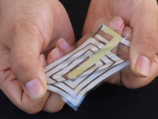
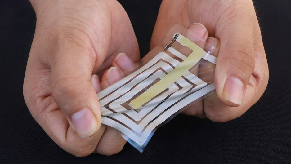
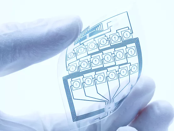
MEMS technology has changed human interaction with electronic devices. Introduced in the 1990s, the first mass-market MEMS devices were used for inkjet printheads and automotive airbag crash sensors. Today, MEMS are ubiquitous, with billions of the tiny devices adding intelligence and interactivity to smartphones, smart speakers, wearables, automobiles, biomedical devices, remote monitoring and event detection systems, and countless other applications. Integrating MEMS with Flexible Hybrid Electronics (FHE) is an important step in the evolution of this miniaturized intelligent sensing technology, paving the way for its use in new classes of flexible, conformal devices.The integration of the two technologies promises to breed new applications in small form factors but also presents challenges inherent to FHE design and fabrication processes. SEMI’s Nishita Rao caught up with Nathan Pretorius, prototyping and automation engineer, NextFlex, to discuss MEMS-FHE device integration challenges and opportunities ahead of his February 26 presentation, Integrating MEMS Devices in FHE, at FLEX|MEMS Sensors Technical Congress (MSTC) 2020, February 24-27, 2020, at the DoubleTree by Hilton in San Jose, California.Join us at FLEX|MSTC to meet Nathan and other industry influencers advancing innovation in FHE and MEMS sensors. Register now to connect with him at FLEX|MSTC or visit him on LinkedIn.SEMI: Why is integrating MEMS devices into FHE systems important? What new use cases might it enable?Pretorius: The main value proposition of integrating MEMS devices into FHE is that it allows MEMS devices to exist in a different form factor than was possible previously, giving us high-quality MEMS sensors on the flexible and conformable platform of FHE.Ease of application, flexibility, lower cost and rapid iteration on a design are just some of the benefits of FHE devices. And because there are few robust FHE sensors that overlap with MEMS’ capabilities, when you combine the two, you get a lot of compelling uses. That’s why NextFlex is working with agencies and companies to evaluate MEMS’ integration, including using bare MEMS die with microfluidics and promoting new ways of attaching and packaging MEMS die for use with FHE. SEMI: Why is FHE an ideal platform for integrating various types of sensors?Pretorius: MEMS integrated with FHE devices are ideal for rapid design and deployment of data-gathering sensor nodes — which we can iterate for specific applications. A few examples include on-body health monitoring devices for bio-fluids analysis, medical pressure sensors for monitoring blood pressure, and peel-and-stick sensors nodes for infrastructure monitoring. In terms of design and production, FHE devices support rapid prototyping, allowing for instantaneous design-iteration cycles. This speeds design-to-production over traditional rigid PCBs and copper flex because the feedback cycle time between design, manufacturing and testing is shorter, accelerating time to market. What’s exciting about FHE technology is that a variety of sensors or components, including MEMS, can be designed into the base system to easily customize it for a specific application. In addition, our experience shows that when compared to a traditional rigid PCB, an FHE board reduces manufacturing steps and device weight by two-thirds and, perhaps most importantly, converts the device to a thin, conformal shape that makes possible products in new form factors. SEMI: What are the primary challenges to integrating MEMS with FHE? What is NextFlex doing to help device manufacturers address these challenges? Pretorius: There are a few challenges, some of which are device-specific. Most recently, I’ve been focusing on inertial and timing devices, including accelerometers, gyroscopes and resonators. There are a few technical challenges involved in the process of getting the devices from the wafer to an FHE substrate. The wafer processing is very important, especially the dicing and thinning steps. After thinning and dicing, the die is placed onto the FHE substrate. The stresses caused by bonding to the substrate have to be understood and characterized. After placing the die, you then have a calibration step, which is normally performed after the device is packaged. With a MEMS die placed onto directly onto an FHE substrate, calibration then must be done.Finally, the device encapsulation is important, since on an FHE substrate the hard-to-soft material transition is very important to mitigate stresses to rigid component interfaces. We have also been looking at how to work with devices that have damping vents. Flexible encapsulants are inherently more permeable to gases and water vapor than hard encapsulants, so studying the encapsulation of MEMS devices on FHE is another area of interest. NextFlex has been working in a supporting role to evaluate best design practices and best attach and integration methods. In addition to our ongoing collaborative programs, NextFlex is developing the FHE manufacturing ecosystem to include system and component manufacturers and designers, product developers, and materials and equipment providers.SEMI: How do we facilitate closer collaboration between the FHE manufacturing ecosystem and MEMS suppliers such as MEMS device manufacturers, product developers, and materials and equipment providers?Pretorius: It’s important to include manufacturers early in the design process so we can identify challenges up front. That’s why NextFlex spearheads technology road-mapping efforts that include representatives from across the manufacturing ecosystem. We use the roadmaps to prioritize challenges that we can address effectively through collaboration, focusing the industry on solving problems through Project Calls that reveal integration challenges and results from real devices and that tell us how the materials and equipment actually perform with a real device.NextFlex keeps the information flowing, holding quarterly project update webinars to share results. As current devices are optimized for the process in which they will be used, we learn a lot from the project performers who make FHE system demonstrators — and we share that information with the member community. SEMI: Can you point to an example of a successful MEMS-FHE device integration?Pretorius: MEMS-FHE integration is still in the early stages, but we are working on several projects including a DARPA Seedling project for which we have integrated MEMS sensors into FHE systems for testing and evaluation. We plan to continue this work by integrating MEMS and FHE devices using methods that support mass production.SEMI: What would you like FLEX|MSTC attendees to take away from your presentation?Pretorius: We would like to see the FHE community work more closely with MEMS device manufacturers. For example, NextFlex often works with manufacturers to gain access to bare die, which is still a significant hurdle in making devices.The best way to speed things along is to get involved. We encourage FLEX|MSTC attendees to join NextFlex. As a prototyping and automation engineer at NextFlex, Nathan Pretorius explores new print methods for prototyping and automation using novel materials and processes. Pretorius currently focuses on how best to apply software scripting and machine learning to streamline FHE processes. Prior to joining NextFlex, he researched the strengths of roll to roll and screen printing on printed electronics designs, including capacitive touch interfaces, FHE passive component design, and antennas. Nathan holds a Bachelor of Science degree in Graphic Communications from Clemson University. FLEX|MSTC is organized MEMS Sensors Industry Group (MSIG) and FlexTech, SEMI technology communities focused on the growth of MEMS sensors and the flexible electronics supply chain, respectively.Nishita Rao is marketing manager for technology communities at SEMI.
Read More
VTT Technical Research Centre of Finland Ltd (VTT) has its sights set high. As a leading global research and development firm , VTT is out to produce bio-interfacing and biodegradable flexible hybrid electronics (FHE) devices that help tackle some of the world’s greatest challenges including environmental degradation and food scarcity.SEMI’s Maria Vetrano interviewed Antti Vasara, president and CEO of VTT Technical Research Centre of Finland, to preview his February 25 keynote, Beyond Flexible Hybrid Electronics: Biodegradable Electronics and Interfacing Bio+Electronics, at FLEX|MEMS Sensors Technical Congress (MSTC) 2020, February 24-27 at the DoubleTree by Hilton in San Jose, California. Join us at FLEX|MSTC to meet Antti and other industry influencers driving innovation in flexible hybrid electronics (FHE) and MEMS sensors. Register now to connect with him at FLEX|MSTC or visit him on LinkedIn.SEMI: What is body-interfacing electronics and what is your vision for bio-interfacing and biodegradable electronics?Vasara: Body-interfacing electronics have existed for decades. Developed in the 1970s, the wireless heart rate monitor is a good example. While continuous heart monitoring with a compact, inexpensive wearable device is widely accessible technology, other bodily parameters, such as cholesterol levels or biomarkers, are diagnosed every time we see a doctor. Establishing a baseline using multiple measurements — before symptoms develop is actually much more effective.That’s where bio-interfacing comes in. Bio-interfacing devices will continuously measure and analyze complex biogenic substances such as sweat, breath, blood and urine. A smart patch for continuous sweat monitoring, for example, would overcome several challenges: supporting electronics functionality in liquid environments, managing the transport of harvested samples to and from the sensor, managing potential contamination, and disposing of samples after measurement.While FHE in principle delivers the right building blocks and is an ideal form factor for a wearable sweat analytics patch, flexible circuits are not ready for out-of-the box interaction with biological matrices. Hence, our mission at VTT is to anticipate and develop the upscaling process know-how required for FHE devices that either interface with biological systems — or that must themselves biodegrade.We’re also focusing on biodegradable electronics because environmentally conscious end-users and manufacturing companies want biodegradable versions of energy-autonomous, label- or sticker-like Internet of Things (IoT) sensors. Typically used for packaging, logistics, environmental monitoring and medical diagnostics applications, these sensors — which have a lifetime of a few days, weeks or months — have become very popular. Unless they are biodegradable, however, they just add to landfill.SEMI: What approaches is VTT using to develop bio-interfacing and biodegradable electronics?Vasara: In our Business Finland-funded ECOtronics project, we are working with our partners to create recyclable and compostable electronics and optics that use renewable resources. For example, devices developed using substrate materials like paper, cardboard or VTT’s in-house-developed nanocellulose films and biopolymer films for environmental monitoring or skin patches can be easily recycled or even biodegrade naturally. Where possible, we use roll-to-roll printing to generate the device circuitry, and on a component level, we have optimized our assembly process towards bare-die component bonding to reduce the overall footprint of non-biodegradable waste per device.SEMI: What use cases do you find most promising and why?Vasara: A prominent example of a single-use test that generates a large amount of waste is the digital pregnancy test. When breaking it down into components, you will find a rigid circuit board with microprocessor, a couple of coin cell batteries, a liquid crystal display, a LED light source and photodiode, and a large chunk of plastic packaging around it. The materials and battery capacity of such a device would be sufficient to run hundreds of pregnancy tests – actually technical overkill.By using printed circuits on biodegradable substrates, bare-die assembled components (ASIC, LED light sources, photo diodes, thin film batteries as power sources) and device packaging composed of biodegradable plastics, we can completely redefine the environmental footprint of single-use tests. We are currently developing a toolbox for our customers to turn their existing conventional test into an ecotronic form factor.Another exciting use case is a sweat sensor that we developed collaboratively with Ali Javey, Ph.D., professor of Electrical Engineering and Computer Sciences, UC Berkeley, and the co-director of Berkeley Sensor and Actuator Center (BSAC). Together with his team, we created a wearable electrochemical sensor for continuous sweat analysis during exercise. With the UC Berkeley group providing the chemistry to monitor N+, K+ ion and hydration levels in sweat over the duration of several hours, VTT delivered the underlying sensor platform, featuring the printed sensor electrodes and sweat harvesting microfluidic channels for fluid management and transport. It’s exciting to see what we can achieve by combining techniques from different disciplines, in this case electrochemistry, printing, packaging and microelectronics.SEMI: How can industry enable the development/manufacture of flexible FHE devices? Where does VTT fit into the ecosystem?Vasara: As many FHE devices target large-volume markets, scalability of manufacturing is key: How can I get from one device (= working prototype) to a handful of devices (= feasibility study), to thousands (= pilot manufacturing), to a million (= mass manufacturing) without compromising the quality of the system’s performance and reliability?Access to upscaling infrastructure is essential for the development of novel FHE devices and methods, but infrastructure is expensive. That’s where our establishment of a roll-to-roll pilot printing line to bridge the gap between laboratory R D and mass manufacturing has proved invaluable. We can provide a unique worldwide upscaling infrastructure for advanced FHE devices, with a strong focus on large-area roll-to-roll processes and hybrid assembly. This service removes our customers’ burden of high infrastructure investment in early development stages and it allows us to guide customers along their development path, from prototype to mass production.Watch our video: VTT pilot manufacturing for diagnostics and wearablesSEMI: Is there anything else that device manufacturers need to know in order to succeed?Vasara: In my eyes, the success of FHE devices eventually depends on several factors: It requires a high degree of automation, well-optimized processes, reliable supply chains, and perhaps most importantly, clear standards and rules for designers to guarantee flawless interoperability of all the different elements on a flexible and hybrid circuit. Let us not forget – we are trying to marry electronics with printing, biology, packaging, microfluidics, injection molding and other fields of expertise.We recently finalized the compilation of a set of design rules for publication in our state-of-the-art overview of printed and hybrid electronics manufacturing methods. You can download the overview, PrintoCent Handbook, for free.SEMI: What would you like FLEX|MSTC attendees to take away from your presentation?Vasara: The latest technologies and innovations in microelectronics, MEMS, printing, materials, and biosensors provide us a toolbox for true innovation in the FHE space. Now we need cross-disciplinary thinking and daring steps to combine different manufacturing methods and skill-sets. The ideal cross-disciplinary team might include: The printing engineer who knows how to design contact pads for a bare-die IC assembly The biologist who knows about the thermal and mechanical stress in a printing environment to design processes for bio-functionalization of surfaces The electronics engineer who knows how to optimize a circuit powered with an enzymatic biofuel cell The number of sensors deployed on (or inside) our body, in our drinking water, in our cars, on our fields, in our pets, and everyday products will surely grow. Let us make sure they leave the smallest environmental footprint possible.Antti Vasara, Ph.D. has been the president and CEO of VTT Ltd since 2015. VTT is a visionary research, development and innovation partner with over 2000 people and a turnover exceeding 250M EURO. Vasara is president of EARTO (European Association of Research and Technology Organisations) and is chairman of the board of Palta (Finnish Service Sector Employers). In addition, he is a non-executive director of Elisa Oyj (largest communications operator in Finland) and a board member at EK (Finnish Confederation of Industries).He has served on several high-profile groups on industrial and innovation policy of the European Commission, in addition to several groups in Finland on artificial intelligence and research policy. Previously, Vasara spent close to 25 years in private industry, working at Nokia, Tieto, SmartTrust and McKinsey Company. Earlier in his career, he was a researcher in optical communications with 20+ peer-reviewed articles and one international patent. Vasara holds a Doctor of Science (Technology) degree from Aalto University in Finland.For more information about VTT’s work in bio-interfacing and biodegradable FHE devices, visit VTT Research. FLEX|MSTC is organized MEMS Sensors Industry Group (MSIG) and FlexTech, SEMI technology communities focused on the growth of MEMS sensors and the flexible electronics supply chain, respectively.Maria Vetrano is a public relations consultant at SEMI.
Read More
Part 2 of 2-part series on MSEC 2019 highlights. Read Part 1. Neural Networks on ChipTo be sure, low power is king when bringing machine learning to the sensor edge. Battery-powered, always-on sensing devices require it since frequent recharging is the death knell of any electronic product. That’s why semiconductor companies are offering new ways to conserve power.“MEMS sensor suppliers have made significant strides in the power, size and performance of their devices,” said Aspinity CEO Tom Doyle. “Yet these gains deliver only incremental power improvements to the system.”Doyle advocates a new architectural model that uses an analog neuromorphic processor to analyze all sensor data at the start of the signal chain instead of sending it downstream so power-hungry chips such as DSPs can digitize it before analysis.“The technology industry wants to take advantage of the many benefits of always-on sensing applications,” said Doyle. “Before we can reach mass proliferation, however, we need to resolve the power issues that are deal-breakers for some applications. We believe the answer to this challenge is architectural. All the data gathered by always-on sensing systems is analog in nature, yet as soon as it’s captured, it’s digitized immediately for analysis. Determining which data is important up front eliminates the digitization and processing of irrelevant data so that voice-first devices such as smart speakers and wearables/hearables can run for long periods of time without requiring battery recharge.”Syntiant CTO Jeremy Holleman agreed that on-device intelligence is the future.“Did you just fall? Is your heartrate a bit off? Deep learning provides a toolset that yields vastly superior decisions,” said Holleman. “The problem is that deep learning is computationally intensive. The answer is a neural network that performs on-device edge inferencing.”Holleman added that Syntiant’s neural decision processor was recently certified as Amazon Voice Service (AVS)-compliant for wake-word detection, making it easier to design voice control in battery-powered devices such as earbuds and wearables.MSEC Technology Showcase WinnerWith the groundswell of interest in intelligence at the edge, it was no surprise that Cartesiam won top honors among all competitors in the MSEC Technology Showcase for its NanoEdge AI, software that brings AI to the edge of the signal chain, making it easier for designers to create intelligent objects that can learn and understand.“Unlike other AI algorithmic technologies for sensing devices, NanoEdge enables both learning and inference at the edge, providing accurate and adaptive intelligence,” said Cartesiam Managing Director and Co-founder Marc Dupaquier, who accepted the award. “It’s also the only tool of its kind that does not require data scientists on board for implementation, which saves a tremendous amount of money. Our clients can build a machine learning library and embed it into their own code within weeks to realize the same caliber of unsupervised neural network that was once the exclusive domain of AI cloud vendors.”MSIG 2019 Hall of FameAt this year’s conference, MSIG Director Carmelo Sansone recognized two longtime contributors to the commercialization of MEMS and sensors: Peter G. Hartwell, Ph.D., chief technology officer at InvenSense, a TDK group company; and Thomas Kenny, professor and senior associate dean of engineering at Stanford University.Hartwell leads technology strategy and the InvenSense advanced technology research group. He has more than 25 years’ experience commercializing silicon MEMS products, including advanced sensors and actuators, and developing MEMS testing techniques.Kenny’s academic accomplishments include authoring or co-authoring more than 250 scientific papers and holding 50 issued patents. He has also advised more than 50 graduated Ph.D. students from Stanford.MSEC 2020Mark your calendar for next year’s MSEC, October 12-14, at Coronado Island Marriott Resort Spa in Coronado, Calif. Get updates from MSIG on MSEC and other upcoming events including MSTC 2020.Stay in Touch with MSIGMEMS Sensors Industry Group (MSIG), a SEMI Strategic Association Partner, is the industry association representing the global MEMS and sensors supply chain. To learn how MSIG enables professionals in the MEMS and sensors industry to innovate, address common challenges and accelerate business results, visit us today.Connect with MSIG on Twitter and LinkedIn. Subscribe to SEMI Blog: Technology and Trends.Maria Vetrano is a public relations consultant at SEMI.
Read More
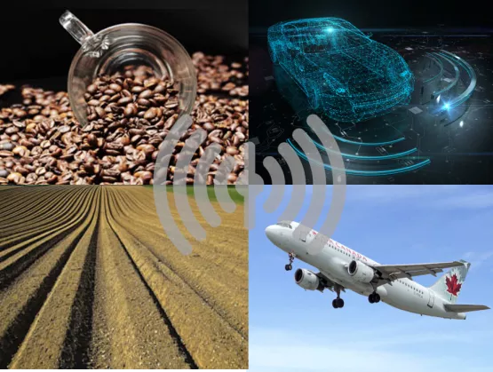
Part of 1 of 2-part series on MSEC 2019 highlights. Read Part 2. MEMS and sensors are proliferating across consumer, automotive, biomedical/healthcare, robotics, industrial and agriculture applications to harvest sensory data in a hyper-connected world and meet demand from consumers and organizations alike as they clamor for more intelligence in electronics.Take the ubiquitous iPhone. Shipped in 2007, Apple’s first iPhone sported five sensors. By contrast, the most feature-packed smartphones will embed up to 20 sensors by 2021, according to Yole Développement’s Jérôme Azémar. He estimates that the devices will feature four MEMS microphones, four CMOS image sensors (CIS), a RGB color sensor, a laser rangefinder, an infrared sensor, a gas sensor, a heart rate monitor and a fingerprint sensor, not to mention the MEMS inertial sensors that device users have come to know and trust.The MEMS market is expected to reach $18.5 billion in 2024 [1], up a whopping 60 percent from $11.6 billion in 2018, according to Azémar, who presented at MEMS Sensors Industry Group’s 15th annual MEMS Sensors Executive Congress (MSEC) in late October in Coronado, Calif. Add other types of sensors to the mix – CIS, environmental sensors, LiDARs, radars, ultrasonics, and fingerprint sensors – and the market will mushroom to $93 billion by 2024, said Azémar.Since MEMS Sensors Industry Group (MSIG) joined SEMI as a Strategic Association Partner three years ago, SEMI has expanded its MEMS and sensors programs to Europe and Asia while continuing to grow its U.S. conferences. “SEMI is continually investing in MEMS and sensors innovation across the supply chain,” said Dave Anderson, president of SEMI Americas and host of MSEC. “For example, MSIG is contributing to the development of the Heterogeneous Integration Roadmap, an initiative designed to drive heterogeneous integration technology development and accelerate electronics innovation. The roadmap spans device design, test and fabrication, ecosystem development, R D, equipment and materials. “At MSEC, executives and other speakers explored how AI and blockchain are remaking the food supply chain, air transportation and other sectors as MEMS and sensors improve the quality of our lives,” said Anderson.Sensing at the EdgeThe concept of artificial intelligence (AI), that a machine can harness intelligence that rivals or outperforms humans – and act without human intervention – has been a feature of the human imagination since at least the 1968 film 2001: A Space Odyssey. MEMS and sensors facilitate intelligence in a wide range of electronics such as smartphones, healthcare wearables, robots, industrial predictive maintenance systems, and cars. AI is sure to augment that functionality.MEMS and sensors are now in their third wave of evolution, a focus on edge AI, Bosch Sensortec CEO and General Manager Stefan Finkbeiner told MSEC attendees. For its part, Bosch is working to add AI to MEMS devices. The first wave integrated software with MEMS sensors, and the second, sensor fusion, enabled designers to allocate performance and power strategically to tune MEMS for resource-constrained devices. The third wave is “an active-learning phase in which MEMS facilitates real-time learning at the edge to promote greater personalization, environmental feedback, privacy of user data and improved battery life,” said Finkbeiner.Small sensor nodes with edge AI exemplify third-wave applications. Integrating low-power environmental sensors (e.g., gas, temperature, pressure, humidity and air-flow sensors), the nodes could be deployed in fire-prone forests to assess fire risk and support early detection. Access to this real-time environmental information could prove invaluable to residents and public-safety personnel alike.Google takes another tack, applying machine learning to resource-constrained devices, said Nick Kreeger, a senior software engineer at the Internet giant. The company’s Google Brain creates machine learning models that can run on inexpensive, low-power microcontrollers using Google’s TensorFlow Lite, an open-source machine learning tool that’s been deployed on a multitude of mobile devices. Inferencing is done at the device’s edge, rather than transmitted to the cloud.Meeting the power constraints of battery-powered sensing devices is another matter that starts with minimizing energy and data waste. “Deep learning is compute-bound and runs well on existing microcontrollers,” Kreeger said. “Because it’s all arithmetic, it’s low-power compared to storage access.”Already Google has worked with Plant Village, a research unit at Penn State University, and the International Institute of Tropical Agriculture (IITA) to help farmers improve food production by using machine learning and cheap sensors to spot and manage planet diseases in developing countries. And that production chain is in dire need of a boost, according to Rajendra Rao, general manager of IBM Food Trust, an enterprise-class blockchain solution.“We are on the cusp of complete failure of the food system,” Rao said. “One out of 10 people gets sick each year from foodborne illness, 420,000 die from this annually, 80 percent of companies in the food supply chain have not digitized, one-third of all fresh food in the US is thrown away, and one in five seafood samples worldwide is mislabeled.”IBM Food Trust’s work with Sucafina, which manages a global green coffee supply chain, shows how sensors can trace food from the farm to the processing plant to the consumer. With the IBM Food Trust platform, Sucafina can track the origin of the beans used in a cup of coffee – a competitive differentiator to coffee drinkers eager to support fair-trade coffee roasters.ripe.io, one of Forbes’ 25 most innovative AgTech startups, is also tackling the challenges and complexities of the food supply chain.“Our secure blockchain platform creates a digital twin of food items, transparently aggregating foods’ journey in real-time, to provide a harmonized trustworthy platform for multiple stakeholders,” said Rachel Gabato, the company’s COO. The ripe.io blockchain-based platform collects data from various sensors – temperature, pressure, light, humidity and inertial MEMS sensors. Growers, distributors and end customers including sweetgreen – a U.S. restaurant chain that depends on fresh produce – use the information to trace the origin and quality of food.MSEC 2020Mark your calendar for next year’s MSEC, October 12-14, at Coronado Island Marriott Resort Spa in Coronado, Calif. Get updates from MSIG on MSEC and other upcoming events including MSTC 2020.Stay in Touch with MSIGMEMS Sensors Industry Group (MSIG), a SEMI Strategic Association Partner, is the industry association representing the global MEMS and sensors supply chain. To learn how MSIG enables professionals in the MEMS and sensors industry to innovate, address common challenges and accelerate business results, visit us today.Connect with MSIG on Twitter and LinkedIn. Subscribe to SEMI Blog: Technology and Trends.[1] Source: Status of the MEMS Industry report, Yole Développement, 2019Maria Vetrano is a public relations consultant at SEMI.
Read More
Software for sensors has evolved from simply reading out and evaluating sensor data to making intelligent decisions based on that data, a transformation enabled by new software synthesis and artificial intelligence (AI) technologies. Together, they make consumer devices smarter, dramatically improving the user experience through greater interactivity and higher levels of automated personalization.SEMI’s Nishita Rao spoke with Stefan Finkbeiner, CEO and General Manager at Bosch Sensortec, who will explore the topic in his October 23 keynote, How Software Makes MEMS Sensors into Smart Systems, at MEMS Sensors Executive Congress (MSEC), October 22-24, 2019, at the Coronado Island Marriott Resort Spa in Coronado, Calif.Join us at MSEC to meet Bosch Sensortec and other industry influencers driving MEMS and sensors innovations. Registration is open.SEMI: What is the relationship between MEMS sensors suppliers and specialized software synthesis providers?Finkbeiner: Collaboration is a key driver for innovation in sensor software. There are already several fruitful collaborations between MEMS sensors suppliers and specialized software providers, which are mostly startups. Collaborations with providers of simulation and evaluation tools as well as with well-known universities in the field of AI are starting to show positive results.Domain expertise is also critical for developing smart sensor software, making it essential to future sensing solutions.SEMI: How does software synthesis relate to sensor fusion?Finkbeiner: Put simply, software synthesis refers to ways of automatically generating code based on domain knowledge and given constraints for specific product versions. Sensor fusion combines sensor data from different kinds of sources in order to improve the results.Software synthesis techniques enable a level of automation that creates new opportunities for more complex sensor fusion, which was formerly out of reach when using traditional approaches that involved, for example, big data and a large number of potential data sources.The traditional sensor fusion toolset can now be further extended by machine learning techniques that help to determine which sources are more reliable than others and how to combine data streams. This topic and others are still active areas of research. A wearable device with motion detection is a case in point. With unsupervised learning, the device could identify short versus long cyclically repeating motions and treat them differently from other types of motion. SEMI: How is the new software synthesis-AI approach different from previous approaches? To what degree will the new approach open up new applications?Finkbeiner: Traditionally, technology companies have used cloud computing for data storage and machine learning on aggregated user data. In that model, MEMS sensors generate large amounts of data that power-hungry hardware (such as digital signal processors) must process. In addition, machine learning generally requires lots of power-hungry cloud nodes with GPUs. This model, however, is not the best option for many users. Just think for a moment about all the scenarios in battery-powered devices where frequent battery charging frustrates users.Leveraging both software synthesis and AI techniques in MEMS sensors is therefore a very promising approach because it supports improved recognition and learning inside the sensor. This means that user-specific data isn’t transferred to the cloud. Instead, it remains private inside the sensor. This improves existing applications that learn all the time and opens up new opportunities for applications such as smart clothing, predicting a product’s lifespan, detecting whether a window or door is open or closed – all without server connectivity.SEMI: How will such software adapt to the individual user?Finkbeiner: Devices will offer much more personalized information to users. For example, optimizing a step counter to match the height, age or Body Mass Index (BMI) of a user – or to adapt to a user’s environment (is the person running on a beach, hiking up a mountain or strolling in a park?) – will provide more accurate information on calories burned. Not every step is created equal, and both pre-loaded personal data as well as real-world environmental data will prove that some steps consume a lot more energy than others.SEMI: What would you like MSEC attendees to take away from your presentation?Finkbeiner: I want to introduce the journey of software development by illustrating specific use case examples. I would also like to offer my outlook on the role of software and AI in MEMS sensors to help increase their adoption in current and new applications. Ultimately, I think it’s important to raise awareness in our industry on why we should embrace the use of software and AI.Connect with Stefan Finkbeiner at MSEC or via LinkedIn. Get more information on Bosch Sensortec products and solutions online.Stefan Finkbeiner, Ph.D., CEO and General Manager, Bosch Sensortec, was appointed CEO of Bosch Sensortec in 2012. He joined the Robert Bosch GmbH in 1995 and has been working in different positions related to the research, development, manufacturing, and marketing of sensors for more than 20 years. His senior positions at Bosch have included director of marketing for sensors, director of corporate research in microsystems technology, and vice president of engineering for sensors.Finkbeiner received his Diploma in Physics from the University of Karlsruhe in 1992 before studying at the Max-Planck-Institute in Stuttgart, where he earned his Ph.D. in Physics in 1995. In 2015, Finkbeiner received the prestigious lifetime achievement award from the MEMS Sensors Industry Group (MSIG), a SEMI technology community.Bosch Sensortec is a member of MEMS Sensors Industry Group, the industry association representing the global MEMS and sensors supply chain. To learn more about how MSIG enables professionals in the MEMS and sensors industry to innovate, address common challenges and accelerate business results, visit us today.Nishita Rao is marketing manager for technology communities at SEMI.
Read More
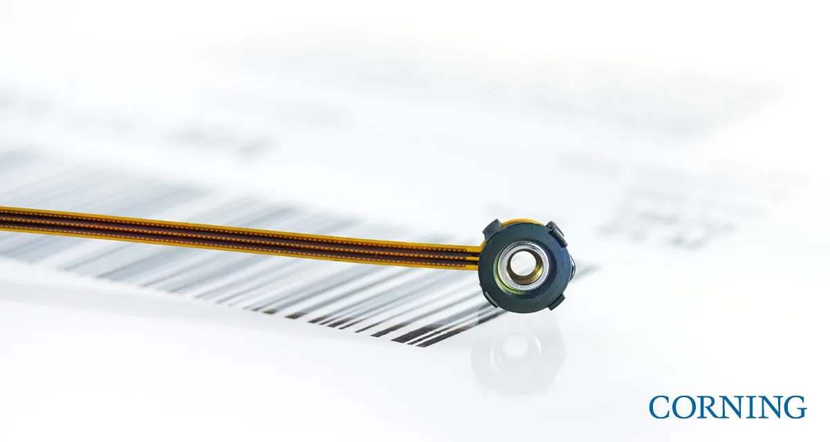
The evolution of industrial and non-industrial automation, smart manufacturing, and Industry 4.0 technologies have increased demand for vision systems that support robust, reliable imaging industrial applications. What factors are driving growth in the machine vision market today?SEMI spoke with Frederic Laune, Business Manager, European Technology, Corning, about how Corning® Varioptic® Lenses are vital to advancing the speed, efficiency, and integration of products using computer imaging. Laune shared his views ahead of his presentation at SEMI MEMS Imaging Sensors Summit, 25-27 September, 2019, at the WTC in Grenoble, France. Join us at the event to meet Corning and many other key industry influencing players. Registration is open.SEMI: Corning's markets include optical communications, mobile consumer electronics, display technology, automotive, and life sciences vessels. Back in June 2019, Corning Incorporated announced that it had delivered its 2 millionth Corning® Varioptic® Lens for industrial applications. What drove this great milestone?Laune: This milestone was met thanks to the fact that Corning Varioptic’s solution solves several problems generated by classical motorized solutions used in industrial applications: limited number of actuation cycles, poor vibration and shock resistance, size (meaning bulky), and high-power consumption. Before Varioptic, there was no variable focus solution that worked well.In addition, the explosion of the CMOS sensor technology helped drive down the cost of imaging solutions for industrial devices, increasing the number of applications and shipping volumes.SEMI: What inspired Corning Varioptic Lenses?Laune: Varioptic was started in 2002 by Dr. Bruno Berge, a French physicist turned entrepreneur. Inspired by the work of Gabriel Lippmann, the 1908 Nobel Prize winner for the invention of color photography, Dr. Berge explored the shape-altering effects of an electric charge when applied to two liquids, a phenomenon referred to as electrowetting. His research ultimately led to the creation of liquid lenses.Fast forward to 2017, when Varioptic became a part of Corning through an acquisition that included Varioptic and Invenios technologies. We believe the synergies from this acquisition will lead to exciting new liquid lens application opportunities that align with Corning’s growth strategy and core capabilities. Corning is one of the world’s leading innovators in materials science. For more than 165 years, Corning has applied its unparalleled expertise in glass science, ceramic science, and optical physics to develop products that transform industries and enhance people’s lives.SEMI: What differentiates traditional camera systems from adjustable lens solutions?Laune: Traditional industrial cameras are usually fixed focus, meaning that the image is sharp only in a limited distance range. Unlike consumer camera applications, there were no good solutions for variable or auto focus cameras in the industrial space. This is due to the intrinsic limitations of motorized technologies.Therefore, customers were using, for example, several cameras to focus at several distances. This compromises the optical quality by closing the objective in order to increase the depth of field, therefore limiting resolution and leading to a need for more light.The cameras using Corning Varioptic’s technology offer more functionality with their ability to focus, whatever the distance, in a fast, reliable, and accurate fashion, and with lower power consumption than traditional mechanical solutions. The upshot is that the product that can withstand heat, vibration, mechanical shocks, and high numbers of focus cycles in tough industrial environments. SEMI: And how is electrowetting enabling industrial devices to capture images and process information quickly and clearly? Laune: In two words: fast and accurate.Electrowetting has unique features – with our two-liquid solution, we combine fast focus with high vibration and shock resistance, and the added benefit of low power consumption.What’s more, our programmable lens can be reconfigured on demand. The lens adapts rapidly and continuously from diverging to converging and can be modeled to support demanding variable focus applications. Our lenses can change their focus in milliseconds, similar to the human eye, and capture fast-moving objects at varying distances. The use of liquid, over mechanical solutions, allows us to create a small form factor, saving precious space and reducing power consumption.SEMI: What industrial applications are taking advantage of this technology? Can you name one example?Laune: 2D barcode readers and industrial vision are our main markets. There is also a strong adoption of our technology in medical applications.SEMI: What does the rise of machine vision mean for manufacturers? Give us one prediction about the opportunities offered by advanced imaging applications.Laune: A great example is the use of 2D barcode readers and liquid lenses to track your ecommerce order, point to point. Another example is full product traceability by implementing a 2D barcode on every component of a given product globally to improve product quality. The varying and adjustable focus abilities of our liquid lens technology make it possible for barcode scanners to track products of different heights, allowing manufactures to improve their processes and logistics.Beyond these examples, tracking and analyzing are booming, thanks to the combination of low-cost CMOS sensor technology, increasing processing power, innovative algorithms (deep learning, AI, neuromorphic processors, etc.), and better image quality due to the progress of lens technology, Varioptic being one.We see an opportunity to improve people’s lives, such as enabling better analysis of medical images and improving the use of cameras in biomedical technologies.SEMI: Quality inspection and automation, adoption of Industrial 4.0 technologies, government initiatives. If you were to choose one, what main factor will drive growth in the machine vision market?Laune: It is difficult to pick just one. I believe that full traceability (monitoring individual parts throughout the production process) has interesting implications as compliance and regulatory efforts ramp up and stronger security of goods becomes more important, particularly as consumers become engaged in food safety and tracing products throughout the supply chain.SEMI: What are your expectations for the SEMI MEMS Imaging Sensors Summit and why would you invite your peers to attend? Laune: I strongly believe in the power of human interactions in technology and science! Ideas come from discussions and physical interactions. The SEMI MEMS Imaging Sensors Summit is a great place to network, meet people, and think about the future! Frederic Laune is the business manager leading the Corning® Varioptic® Lenses business. Laune joined Varioptic as an R D engineer in 2003 after spending the first eight years of his career developing novel active components for the optical telecom industry. At the time, Varioptic was a newly created start-up aiming to develop liquid lens technology for industrial applications. After designing the first two Varioptic commercial products, the Arctic 320 and Artic 416, Laune stepped up as head of Varioptic’s R D department to focus on product and performance improvements. In 2010, he was appointed sales and marketing lead for the company. Varioptic was acquired by Corning Incorporated in early 2017. Laune received a master’s degree in physics and optics from University Pierre and Marie Curie (Paris) in 1995.Serena Brischetto is a marketing and communications manager at SEMI Europe.
Read More
Despite market saturation and stagnation saddling many business sectors, MEMS remains a shining star in the semiconductor industry. Opportunities in automotive, consumer electronics, mobile, medical are rising. What is supporting this industry growth? Who are the big players on the horizon?SEMI spoke with Dimitrios Damianos, Technology Market Analyst, Photonics, Sensing and Display division at Yole Développement, about MEMS market dynamics and future trends. Damianos shared his views ahead of his presentation at SEMI MEMS Imaging Sensors Summit, 25-27 September, 2019, at the WTC in Grenoble, France. Join us at the event to meet experts from Yole and many other key industry influencers. Registration is open.SEMI: MEMS and sensors is one of the healthiest industries not only in Europe but globally. Despite a global economic slowdown, the MEMS and sensors is still growing. What is fueling this growth?Damianos: The value of the global MEMS and sensor market will almost double from $48 billion in 2018 to $93 billion in 2024. In 2018 the MEMS and sensor market represented more than 10% of the total IC market, as more and more MEMS devices and sensors, such as MEMS, image sensors, and RF filters, are integrated in end products in consumer and automotive. In particular, the value of the MEMS-only market reached $11.6 billion in 2018, with consumer applications accounting for more than 60% of the total market. From 2019 to 2024 the MEMS market will grow 8.3% annually in value driven by pressure (for TPMS), RF (for V2X 5G communications), inertial (for ADAS) and future MEMS (such as pMUT for ultrasonic fingerprint) (Source: Status of the MEMS Industry report, Yole Développement, 2019). SEMI: How are MEMS shaping the semiconductor industry today? Damianos: MEMS have a make-smarter enabling capability. They are providing context for new applications and services in transportation, mobility, health, and security. Large companies such as Alibaba and Google are considering MEMS as a critical element in their business solution domains covering the upcoming smart home, smart campus, smart city and smart industry applications. MEMS have key features that correspond to these companies’ criteria for accuracy, small size (without performance degradation), low power and always on (e.g. microphones). Furthermore, with the advent of sensor fusion and edge computing, more sensor data can be processed, maximizing the qualitative and useful information about us and our surroundings. This has a huge impact in all markets, especially consumer.SEMI: MEMS foundries performed well thanks to the boom in industrial and medical applications. Who are the big players right now?Damianos: During 2018, all foundries saw their revenue increase. STMicroelectronics, Teledyne Dalsa, Silex, IMT, Micralyne and Philips Innovation Service are important MEMS foundry players that offer services for various MEMS devices used in medical and industrial markets, among others. On one hand, medical applications were driven mostly by microfluidics, flowmeters, pressure and inertial MEMS. On the other hand, industrial applications were driven by inkjet heads, microbolometers and pressure MEMS. The market prospect, however, is huge for RF MEMS and oscillators that will be used in next-generation 5G infrastructure. SEMI: What is the current status of MEMS for automotive applications? What are the related market drivers? Damianos: In automotive applications, accelerometers and pressure sensors still account for the lion’s share in units. Pressure sensors will grow at more than 8% with Tire Pressure Monitoring System (TPMS) implemented in Chinese vehicles in the near future. After 2019 and 2020, with the new Chinese standard, GB 2614, TPMS will become compulsory: 100% of all new vehicles will have TPMS. Also, automotive MEMS could grow quicker than the corresponding car market (currently at approximately 3%). The reason is a higher number of many different MEMS devices that are being integrated in cars, such as MEMS inertial measurement units (IMUs), TPMS, environmental MEMS for gas and particle monitoring in-cabin and microphones for hands-free voice commands.SEMI: After years of decline, the inkjet heads industry is growing again. What other segments are benefiting from MEMS technology applications? Can you name two examples?Damianos: RF MEMS (BAW filters) is also benefiting from applications in smartphones and will continue to benefit with the arrival of 5G. 5G means additional high frequency sub-6 GHz bands that can only be addressed by BAW filters. Moreover, new infrastructure approach using active antennas will create an expanding market for BAW.Another segment is inertial sensors. Inertial MEMS already have a high potential in wellness and fitness wearables and are gaining support for medical wearable applications to monitor patient activity, with the aim to prevent seizure in cases of epilepsy and other mental disorders. Compared to other types of sensors, MEMS is the golden technology for inertial sensors integrated into medical wearables. They are used for rehabilitation systems, activity trackers and assistance living/fall detection. Specifically, the IMU market will continue to grow for consumer and automotive applications as their price and form factor continue to shrink and they replace traditional standalone MEMS accelerometers and gyroscopes. However, the inertial sensor market will mostly grow for smartphone applications (mostly 6DOF, with 9DOF volumes being comparatively low).SEMI: Give us one prediction about the opportunities offered by the MEMS technology. Damianos: Sensor fusion is becoming more and more relevant since billions of MEMS sensors are made every year. The upcoming 5G revolution will make connectivity easier than ever, creating exponentially more data. To make these data meaningful, data processing is mandatory. Big data is an industry born of recent advancements in AI and machine learning, built upon and fueled by a wealth of new data from ever-expanding sensor applications. An upcoming trend is edge computing, with sensors and MEMS driving a new age of technology. Sensors are digitizing the human experience, and as the real and virtual worlds move closer together, it will be sensors that bind them, enabling new experiences for users everywhere. Running AI at the edge, coupled with sensor fusion, will open new applications for MEMS in audio, motion, olfactometry, and imaging. We also expect that new MEMS devices (microspeakers, ultrasonic fingerprint, pMUT) and piezoelectric MEMS technology could rejuvenate the MEMS market. SEMI: What are your expectations for SEMI MEMS Imaging Sensors Summit and why would you invite your peers to attend? Damianos: SEMI is organizing another very successful event, gathering experts from the Imaging and MEMS industries. We are at a turning point of innovation, with many technological advancements in AI, IoT, AR/VR, biometrics, and other areas where Imaging and MEMS technologies are paramount. Yole is excited to hear the thoughts of many high-profile experts on existing activities and future prospects within their organizations. If you are too, then it is an event that you shouldn’t miss!Dimitrios Damianos, Ph.D. is a Technology and Market Analyst in the Photonics, Sensing and Display division at Yole Développement (Yole). Damianos is a member of a Yole team that produces technology and market reports on the imaging industry including photonics and sensors. Damianos holds a MSc degree in Photonics from the University of Patras (Greece). After his research on theoretical and experimental quantum optics and laser light generation, Dimitrios pursued a Ph.D. in optical and electrical characterization of dielectric materials on silicon with applications in photovoltaics and image sensors, as well as SOI for microelectronics at Grenoble’s university (France). He has also authored and co-authored several scientific papers in international peer-reviewed journals. Learn more! Join the webinar on 5th September 2019. Registration is open! Serena Brischetto is a marketing and communications manager at SEMI Europe.
Read More