downloadGroupGroupnoun_press release_995423_000000 copyGroupnoun_Feed_96767_000000Group 19noun_pictures_1817522_000000Member company iconResource item iconStore item iconGroup 19Group 19noun_Photo_2085192_000000 Copynoun_presentation_2096081_000000Group 19Group Copy 7noun_webinar_692730_000000Path
Skip to main content
Default Banner Image

MEMS

Shenyang is on an unwavering path to maturing its integrated circuit (IC) equipment manufacturing industry over the next few decades in response to the Made in China 2025 Strategy. Since the strategy’s introduction in 2015, the city, long a transportation and commercial hub of China's northeast, has built out a complete integrated circuit industrial chain integrating technical research and innovation, components and parts processing, and equipment manufacturing. Its ambition is to compete on the world stage.Shenyang has implemented policies and provided funding to support the development of its IC equipment and related industries to buttress the development of emerging industries. Speaking at the SEMI China Members Day 2019 in Shenyang, Zheng Guangwen, secretary-general of ICMTIA and Shenyang IC Equipment Industry Technology Innovation Strategic Alliance, said that the city, as a key IC equipment industry base in the upstream of China’s industrial chain, hopes to enter the international community in part by leveraging SEMI’s global platform. Zheng Guangwen, Secretary General, ICMTIA and Shenyang IC Equipment Industry Technology Innovation Strategic Alliance More than 150 representatives from member companies gathered at SEMI China Members Day 2019 to discuss China’s semiconductor industry investment and capital dynamics and semiconductor market trends. The event sought to promote stronger communication and interaction between the upstream and downstream of the semiconductor industry chain. The forum was co-sponsored by SEMI China and Shenyang Science and Technology Bureau and co-hosted by ICMTIA and Shenyang IC Equipment Industry Technology Innovation Strategic Alliance. Lung Chu, President of SEMI China Opening the event, Lung Chu, president of SEMI China, set stage for the discussion by noting that global semiconductor industry has been booming since 1957, reaching another record high of $470 billion in sales last year as it faced a critical juncture, with industry growth slowing in the first half of 2019. The slowdown was predictable and is temporary, a natural stage in the industry’s cyclicality. From a macro point of view, the development of advanced technology requires huge investment. There was an obvious gap in investment between enterprises, which often leads to the stronger become much stronger. Under these circumstances, it is very important for China to master key technologies and products during the process of catching up and surpassing. Each region should focus on its strengths.Enterprises should do their own business in a low-key way and keep a prudent and optimistic attitude. The number of SEMI China members has reached a new high. SEMI China is committed to becoming the best partner to realize China's semiconductor dreams. In promoting the development of global semiconductor industry and China's semiconductor industry, SEMI has continuously gathered strength and actively organized rich activities to promote the sustainable growth of Chinese semiconductor enterprises through international cooperation. Zhao Rigang, Director of SCTB, Shenyang Science and Technology Bureau Zhao Rigang, director of SCTB at Shenyang Science and Technology Bureau, pointed to the importance of SEMI’s pivotal role and global influence in cultivating cooperation between international and domestic industries including Shenyang’s IC sector. Speaking at the SEMI China Members Day 2019 in early June, Rigang said the growing importance of chips in China is a key catalyst for Shenyang’s rise as semiconductor sectors domestically and abroad invest heavily in a new generation of information technologies such as mobile Internet, cloud computing, big data, Internet of Things. Kang Jin, General Manager, SMIC Beijing For China’s semiconductor industry to flourish, the region must improve its IC supply capacity just as it has brought its PV industry to full maturation, said Kang Jin, general manager of SMIC Beijing. The key to developing China's integrated circuit industry, he said, lies in building a robust semiconductor supply chain. Zong Runfu, Chairman and General Manager, KINGSEMI Semiconductor Equipment Supply Chain DevelopmentLocalization has enabled KINGSEMI to optimize its technology design capabilities to produce high cost-performance equipment for greater competitive advantage, saidZong Runfu, chairman and general manager of KINGSEMI. While the localization rate of supply chain construction was over 50 percent, the localization rate for front-end equipment is still low. Zong Runfu said localization is imperative not only to lowering costs, but also to ameliorating the supply-guarantee rate, maintaining quality and shortening the delivery cycle. Russell Li, VP of Marketing and Business Development, WLCSP Packaging Solutions for 3D Active Sensing DevicesInternet of Things (IoT), artificial intelligence (AI), 5G and other technologies are starting to become a part of daily life as more sensors find their way into new retail stores and smartphones, a trend that will continue as autonomous transportation begins to take hold, said Russell Liu, VP of marketing and business development at WLCSP. The move to bring more human-like capabilities to technology is driving the implementation of perception function in devices, with passive sensors giving way to active sensors and machines translating the physical world into a 3D view through the eyes of a 3D camera. What’s more, the next generation of IoT devices will feature more integrated processors including signal processors, caches, sensors, photons, RF and MEMS, bringing the challenges of miniaturization to system integration. Liu said miniaturization will only be possible by developing advanced packaging technologies that enable highly integrated processors for mobile devices and intelligent automobiles. Wang Ronghua, VP of Technology, Dalian Xinguan Technology Getting Ready for GaN Power Electronics EraGaN offers excellent performance in optoelectronics, RF and power electronics and will coexist with and complement silicon devices for years to come, said Wang Ronghua, VP of Technology at Dalian Xinguan Technology. However, the industrialization of GaN power devices still faces technical challenges in application, reliability, packaging, epitaxy, device and process – all barriers to market adoption. To overcome these hurdles, GaN power devices must meet the reliability and cost-performance requirements of applications to which they are best suited.Ronghau said that GaN power devices, such as cascade and p-GaN enhanced devices, now support end products, proof that the era of gallium nitride has arrived. “Gallium nitride is quite different from silicon in epitaxy, device design and key technology, which requires close integration of upstream and downstream industry chains for effective promotion,” he said. Billy Feng, Executive Director, J.P. Morgan Is the Semiconductor Industry Still Cyclical? Since 2008, the semiconductor cycle has waned, disrupting the traditional thinking of investors, equipment suppliers and logistics channel providers as investors’ appetite for the chip industry investments has grown, said Billy Feng, executive director at J.P. Morgan. The long-term prospects for the semiconductor industry remain bright. But after reaching historic revenue highs in 2017 and 2018, the industry – and investor expectations – will enter a period of adjustment. Dr. Adam He, Executive Director, CGP Tech Fund The unique gene of the semiconductor industry consists of the blend of its lofty requirements for quality, reliability and consistency; cooperation between upstream and downstream sectors; internationalization; and a powerful ambition to innovate, said Dr. Adam He, Executive Director of CGP Tech Fund. He described Chinese chip enterprises he often encounters as falling into one of two entrepreneurial categories – IC experts and cross-border business people. Both want the answer to "how to make money and how to establish a solid competitive position?” He said. Adam believes that accessing the genes of the semiconductor industry is the answer to both questions and crucial to the maturation of China’s chip industry. The genes must be used to strengthen the Chinese manufacturing and materials sectors. Du Shanshan, Senior Analyst, SEMI China SEMI Market Outlook: Fab Investment, Equipment and Materials Market ForecastsEmerging technologies have sparked explosive semiconductor industry growth, said Du Shanshan, a senior analyst at SEMI China. While the industry will see a slight recession in 2019 due to memory market softness, trade wars and other factors, it is on stable footing for the long run. At the same time, China continues to optimize its IC industry chain, and semiconductor design and manufacturing companies have gradually grown in number. Over the next decade, the average growth rate of China's production capacity is expected to exceed 10 percent. Richard Feldman, VP of Global Expositions and Events, SEMI Richard Feldman, vice president of Global Expositions and Events of SEMI headquarters, presented the new SEMI Asia semiconductor business development plan to members and called on companies in mainland China, Taiwan and Malaysia to participate in SEMICON Europe to strengthen the influence of globalization.After the meeting, participants visited KINGSEMI Co., Ltd., Shenyang Piotech Co., Ltd, Shenyang SIASUN Robot and Automation Co., Ltd., Shenyang Fortune Precision Equipment Co., Ltd. and SKY Technology Development Co., Ltd. The event facilitated communications between upstream and downstream companies. SEMI China Member Day 2019 Group Photo Cherry Sun is a marketing manager at SEMI China.
Read More
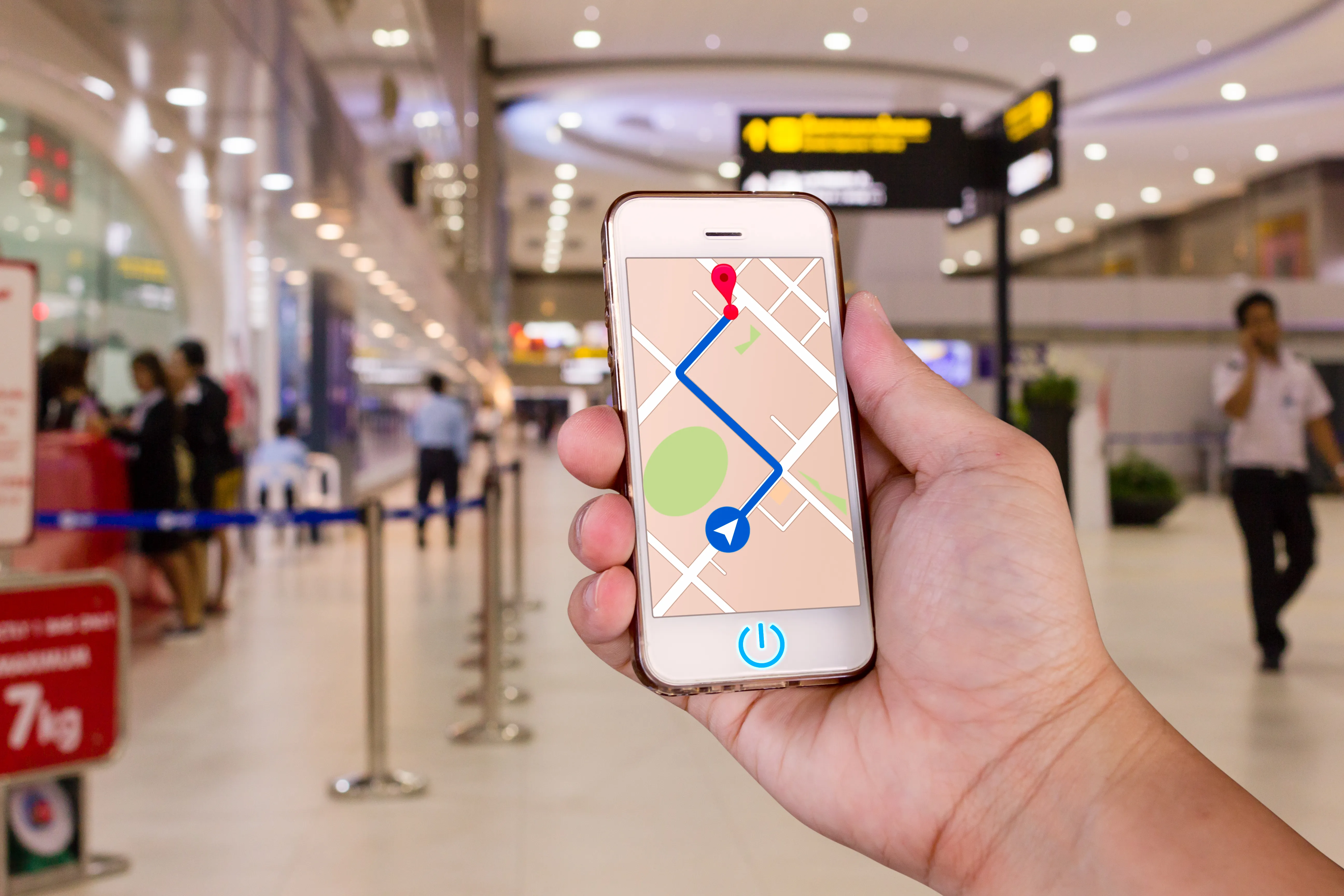
Tracking and localization technologies typically integrate with Wi-Fi and Bluetooth signals to pinpoint the location of people and objects. But what if a venue can’t install beacons or routers, or afford to deploy Wi-Fi or Bluetooth networks? Thanks to a combination of proprietary algorithms, advanced sensor fusion and the natural geomagnetic field, GipStech, a spin-off of Università della Calabria, built an indoor localization and navigation technology platform for accurate localization in the absence of an adequate GPS signal.Ahead of the SEMI MEMS Imaging Sensors Summit, 25 to 27 September 2019 in Grenoble France, Serena Brischetto of SEMI spoke with Gaetano D'Aquila, co-founder and CEO of GiPStech, about sensor fusion, augmented GPS applications and the future of indoor localization. Join us in Grenoble to learn more about GiPStech and meet other MEMS, imaging and sensors experts. Registration is open online.SEMI: Early this year GiPStech completed a test deployment of the first high-precision, infrastructure-free navigation system at Tokyo Shinjuku metro station in Japan. This is the busiest transportation hub globally! What were the main challenges you faced and how did your technology enable such a highly complex indoor localization?D'Aquila: As you mentioned, Shinjuku station in Tokyo has been registered in Guinness World Records as the busiest transportation hub globally. With 36 platforms, 200 exits and countless corridors and connections, it is easy to get lost there, especially for foreigners and tourists. On the other hand, this scale and complexity makes it unfeasible and expensive to install Bluetooth or similar infrastructure for standard indoor localization.For this reason, we needed to provide a cost-effective indoor localization technology without installing any kind of artificial supporting infrastructure. Thanks to our GiPStech patented multi-sensor-fusion localization stack and the high density of public Wi-FI networks, it’s possible to determine when passengers are inside the station. The public Wi-Fi networks signals were fused as an additional source in GiPStech's sensor-fusion platform to complement the inertial and geomagnetic engine and deliver very accurate results across the entire station. The tests performed in the station also demonstrated that the localization system can even detect the floors where travelers are walking. Now we are ready to roll out the same setup in other stations and environments.SEMI: You are not the first to pursue infrastructure-free indoor localization, but your technology platform seems to be very accurate in bringing precision, stability and consistency to the user experience. What lead to those advancements and incredible results?D'Aquila: Our key differentiating factors are built in the approach we created after years of research and development. One differentiation, of course, is related to our expertise and know-how about how the geomagnetic field can be used as a driving signal for the localization process.During R D we constructed and patented a modular multi-sensor-fusion software stack to solve any kind of localization problem, mainly in indoor environments. We started from a single-signal approach based on the employment of the geomagnetic field as a localization signal. But, mainly due to the very inaccurate devices chosen to measure the geomagnetic field, such as the smartphones that everyone carries in their pockets, we noticed that this single-signal approach is accurate but not reliable because it is strongly affected by a key weakness – the quality of sensor in the device.SEMI: How long did it take for you to solve this issue?D'Aquila: We started to integrate other signals within a few months after the first field tests related to the employment of the geomagnetic field alone. We also began to develop a software platform that could fuse any signal source (natural or artificial) available in the environment to preserve the reliability and accuracy of the localization system when some of these signals are temporarily affected by poor measurement quality. This is our differentiating factor today. We can re-configure our software platform to provide the best reliability and accuracy with the lowest artificial infrastructure in almost any context – from outdoor in a seamless way to indoor and vice versa.SEMI: GiPStech’s inertial engine is one of your cutting-edge technologies that completes your advanced indoor navigation and localization software stack. How do you see the technology evolving?D'Aquila: The inertial engine was one of our first technology modules mainly developed to enhance reliability, smooth the signals and reduce the computational power requirement of our geomagnetic localization approach.After a while, together with a third party that evaluated the performances of our module, we noticed that this module not only can be used as a self-standing localization technique, but it can also deliver high accuracy mainly in PDR (pedestrian dead reckoning) applications.Today our PDR is itself a black box with embedded subsystems. Besides some filtering modules, it includes a state-of-the-art step detector that detect steps even when the person changes the smartphone position and location (not only in the hands but also in backpacks or pockets) and an advanced step validation module that identifies and rejects fake steps.If you’ve ever used a commercial fitness tracker attached to your wrist, you know that in most cases if you move your arm the device will counts some steps that, of course, are not real. Our step validator solves this problem by detecting only real steps – a very important capability that allows our PDR to be employed as a self-standing inertial navigation system. We developed the PDR with strong attention to maintaining low requirements for the computational power and memory footprint. These additional characteristics makes the PDR very interesting even for a direct integration of the software at the silicon level in modern MEMS sensors.In a nutshell, the ability of MEMS sensors to run directly an embedded software module will drive technology enhancements that will allow some of the functionalities now available through an external application processor, such as those in smartphones, to move to a lower level (in the silicon). This, of course, reduces power consumption while even increasing the number of value-added services, including localization services, that could be built directly on top of the MEMS without requiring external software and/or application processor.SEMI: Do you think indoor localization will be more applicable in the next 10 years in areas such as Smart manufacturing, travel, healthcare, entertainment and retail?D'Aquila: Several market reports and our business development experience lead us to assess which sectors are of greatest interest for the application of indoor positioning technologies. They include the following. Industry (manufacturing logistics) Healthcare (tracking of assets, patients and doctors) Big installations (visit experience for museums, fairs) Airports stations (both for travelers and for resource and operation management) Large distribution (user profiling and influencing of the purchasing behavior) Indoor localization is a key enabling technology. Adoption, mainly in these sectors, was limited by the unfavorable tradeoff between cost and benefits. Our indoor localization technology aims to overcome those tradeoffs to make its adoption much more cost-effective while providing the best possible reliability and accuracy.SEMI: What are your expectations regarding the summit in Grenoble, and for the future of the sensors technology ahead? Where are we heading?D'Aquila: Many sectors would benefit from indoor localization technologies. MEMS, imaging and sensors are driving innovation and explosive demand for transportation, medical, mobile, industrial and other IoT applications. But these devices also constitute the basic building blocks for the development of reliable and affordable localization technologies.In outdoor environments we are pretty covered by the GPS. Indoors, where we spend more than of 80 percent of our time, similar types of services are coming to the market now and becoming more reliable over time.This Summit facilitates the direct interaction between different stakeholders to act at different points in the MEMS sensors value chain. Indoor localization was an emerging technology unrelated to the sensors ecosystem until now. Today, indoor localization must leverage MEMS sensors to be effective and reliable. In the future, localization technologies will be embedded directly in silicon to deliver the best performance at a lower cost to increase their adoption for more applications.Gaetano D'Aquila served as research fellow from 2002 to 2004 at the CNR and as an assistant teacher at the University of Calabria. From 2003 to 2014, he worked in the industry first as a security consultant for Telcos and Banking in Value Team S.p.A. and then as project manager at Infomobility S.p.A., where he coordinated research and development and strategic activities in the automotive and auto insurance industries. In 2014 he co-founded GiPStech and is its current CEO. He has published several papers in scientific journals and has filed for seven patents, three of which have been granted in the U.S. and Europe. Gaetano has a MSc in Computer Engineering and a Ph.D. in Science and Engineering of the Environment, Buildings and Energy from the University of Calabria, Italy.Serena Brischetto is a marketing and communications manager at SEMI Europe.
Read More
For nearly two decades, Sean Ding, CTO and chief scientist of Alibaba Cloud IoT, has worked in software and algorithm architectures, sensing, semiconductors, systems and cloud computing – all areas that have contributed to the rise of the Internet of Things (IoT). It’s no surprise, then, that Alibaba is leading next-generation innovation for the IoT. Ding will bring his expertise to his role as moderator of Brave New World - MSIG Conference on AI+IoT 2019, a half-day forum March 20, 2019, at SEMICON China in Shanghai, China. Maria Vetrano of SEMI spoke with Ding about technologies key to the IoT era including MEMS, sensors, artificial intelligence (AI), edge gateways and cloud computing. SEMI: MEMS sensors are widely used in IoT devices. What is the relationship between AI and MEMS sensors?DING: While MEMS sensors and AI will increasingly co-reside in end-user devices, I do not recommend adding AI next to the sensor (in the same package). That’s because designers continue to use the ASIC for signal conditioning, so A/D converters are still required. Rather, we should look to edge gateways to carry the majority of the workload, including deep learning, because this reduces system complexity and power consumption.SEMI: Why are smarter sensors shifting data processing and analytics to the edge of IoT devices?DING: Data processing and analytics are very important for IoT devices, but we need to focus on understanding the data, parameter calibration and more. The MEMS sensor industry should leave big data analytics to edge computing and cloud computing because AI requires deep learning, demanding a huge amount of data.The challenge is to find the sweet spot for data processing right next to the sensor element.SEMI: What is China’s evolving role in innovation in MEMS sensors for IoT devices?DING: At present, the MEMS community in China needs to figure out how to innovate instead of copying existing technologies, a low-margin business that will not help to grow the industry. One reason why I am so pleased to see the MSIG Conference on AI+IoT in China is that it will encourage greater creativity in the MEMS community in China, and this will ultimately lead to Chinese companies and R D institutions leading innovation rather than copying it.SEMI: What is the right approach to combining smart MEMS sensors with AI in IoT devices? Why is this important for both domestic Chinese and international markets?DING: Combining data from sensors with cloud-edge computing is the right approach. As sensor companies increasingly provide end-to-end solutions, such as “sensor+ firmware + SaaS + app,” we will realize easier and faster integration of sensors in IoT applications.This is incredibly important because China today is the world’s biggest market for IoT hardware. China has 2,000-plus design houses, 200-plus OEMs and thousands of distributors. That said, we still see a highly fragmented market that will benefit from a faster integration methodology.Faster integration of MEMS sensors and AI/machine learning for IoT hardware will benefit designers in international markets as well.SEMI: What do you hope MISG Conference on AI+IoT attendees will take away from the forum? DING: MEMS sensors are highly fragmented, reflecting the highly fragmented applications in which they play. The MEMS sensors industry should figure out how to provide one-stop-shopping solutions for vertical markets. This will speed the scalability of applications and expedite the growth of sensor production. Sean Ding (柯镇) will moderate Brave New World - MSIG Conference on AI+IoT 2019 at SEMICON China on Wednesday, March 20, 2019, at Kerry Hotel Pudong in Shanghai, China.This conference has been organized by the MEMS Sensors Industry Group (MSIG). Register today to connect with Sean Ding and featured speakers at the event.Speakers at the MSIG Conference on AI+IoT 2019 at SEMICON China include: Welcome and Introduction / 欢迎辞Carmelo Sansone, Director, MEMS Sensors Industry Group (MSIG), a SEMI technology community AI Needs Accurate Data – MEMS Sensors Can Provide It / MEMS传感器为人工智能提供真实数据Andrea Onetti, Group VP of Analog MEMS Group, GM of MEMS Sensor Division, STMicroelectronics Enhanced IoT Edge by Smart Sensors / 智能传感器助力IoT边缘智Bennini Fouad, Regional President Asia Pacific, Bosch Sensortec Horizon AI Processor Solution, Enable Industries in AI Time / 地平线AI芯片解决方案,赋能千万业Carl Zhang 张永谦, General Manager/VP, Smart Chip Solutions Division, Horizon Robotics Inertial Sensors in AI Applications / 运动传感器AI应用案例Ben Lee 李彬 , CEO, mCube Ultra-Low-Power Solutions: an Ecosystem Approach / 超低功耗的生态链解决方案Carlos Mazure, IEEE Fellow, Chairman Executive Director, SOI Industry Consortium High-Integrity, Fault-Tolerant Open Inertial Measurement Platform for AI-based Vehicle Automation / 适用于人工智能车辆自动控制的高集成及容错的惯性测量开放平台Dan Dempsey, Senior Director of Automotive, ACEINNA Maria Vetrano is a public relations consultant at SEMI.
Read More
As group vice president of the Analog MEMS Group and general manager of the MEMS Sensor division at STMicroelectronics, Andrea Onetti brings nearly three decades of experience in MEMS, sensors and audio systems to his leadership role at one of the world’s most successful electronics and semiconductor manufacturers. During his keynote at FLEX and MEMS Sensors Technical Congress 2019, February 18-21 in Monterey, Calif., Onetti will address the criticality of sensor accuracy in advancing automotive, industrial and consumer applications. SEMI’s Maria Vetrano spoke with Onetti recently to give FLEX/MSTC attendees a preview of his presentation. SEMI: What are some promising advancements in sensors for autonomous cars? Onetti: The avionics industry is already successfully applying sensors for autonomous operationl. Inertial navigation systems (INS) support the operation of planes during flight, both after takeoff and before landing. Unfortunately, the technology in these navigation systems is expensive and not scalable, and they are hampered by reliability limitations in an automotive environment.Following the steady progress that we have made with MEMS inertial sensors in consumer applications, we are on the cusp of realizing greater accuracy in temperature and time – finally delivering the performance required for autonomous driving. Because we can scale in production – we’re now manufacturing more than a billion units a year – we can select the cream of this production crop for adoption in cars. Consequently, we should see Level 3 and Level 4 autonomous driving for consumers very soon.SEMI: How are companies using sensors to monitor and track their assets in industrial applications? Onetti: Predictive maintenance and asset tracking are the two main verticals in Smart Industry. The adoption of multiple sensors for condition monitoring is helping to detect the faulty operation of equipment and to detect early signs of issues that are otherwise difficult to capture. Ultrasonic microphones can detect leaks in a pipe at an early stage, accelerometers with high bandwidth can act as micrometers, and accurate temperature sensors can catch overheating. Similarly, in asset tracking, we use temperature monitoring in combination with inertial sensors to detect problems during the transport of goods. Shock sensors with extremely high full scale (up to 8000g) can tell whether a lightweight envelop has been dropped. Pressure sensors can switch off a radio system when a cargo plane takes off and can mute smart trackers in compliance with flight regulations. We really can do almost anything! A full slate of ST sensors and microcontroller units (MCUs) enable WEG’s small but powerful motor sensor, which listens to a motor, feels its pain, and shares that information with engineers, operators and others to diagnose problems before they happen. Image courtesy of STMicroelectronics. High-accuracy motion, environmental and proximity sensors are crucial to VR/AR. Image courtesy of STMicroelectronics. SEMI: How will sensors advance user experiences in consumer electronics, such as VR/AR systems?Onetti: Virtual reality (VR) and augmented reality (AR) are great examples of promising consumer technologies that will become pervasive as performance of inertial sensors improves. First, we need super accuracy in time and temperature to provide the right experience to users. To achieve this level of accuracy, we need a major step forward in performance, and that includes power consumption and miniaturization. Fortunately, we are constantly making progress in the high-accuracy motion, environmental and proximity sensors that are critical to these systems. While the scale is vastly different between VR/AR and automotive, the requirements for AR/VR systems are pretty similar to those that will enable autonomous cars. A growing variety of sensors (environmental, microphone, proximity, motion) – combined with a sensor hub in an MCU – are central to VR controllers (above) and VR head mounted displays (below). Images courtesy of STMicroelectronics. SEMI: We don’t hear much about the criticality of higher accuracy in sensors. Why is improving accuracy in sensors especially important – and what role do calibration routines play in achieving higher accuracy?Onetti: A sensor is more than just the performance of the relevant function. It is also the intrinsic accuracy that it brings. This accuracy is tuned by calibration, which is typically an expensive process done at the end of product manufacturing or – better still – during earlier stages of manufacturing.Today more applications require sensors with higher accuracy, which necessitates investing more time in calibration, leading to higher cost.MEMS technology can help by offering solutions with intrinsic higher accuracy, which reduces the cost of calibration for product manufacturers. This naturally delivers major benefits to OEMs and, ultimately, their customers.SEMI: What would you like FLEX and MSTC attendees to take away from your presentation?Onetti: As attendees explore the wide variety of available sensor solutions for their end products, I would ask them to prioritize the role of accuracy in sensor selection – because improved accuracy means higher quality data, and higher quality data means better decisions with reduced need for data processing.While designers understand the role of calibration routines in qualifying individual components for specific applications, it is the continuous evolution of MEMS technology that offers the best possibility of breakthrough reductions in time and cost of these calibration routines. This makes MEMS sensors more attractive and affordable than similar sensor components based on different technologies. Andrea Onetti will present Accuracy Enables MEMS Sensor Pervasion at FLEX/MSTC on Tuesday, February 19 at 11:00 am.Register today to connect with him at the event. To learn more about STMicroelectronics, click here. Maria Vetrano is a public relations consultant at SEMI.MSTC FLEX 2019 is organized by MEMS Sensors Industry Group (MSIG) and FlexTech.Maria Vetrano is a public relations consultant at SEMI.
Read More
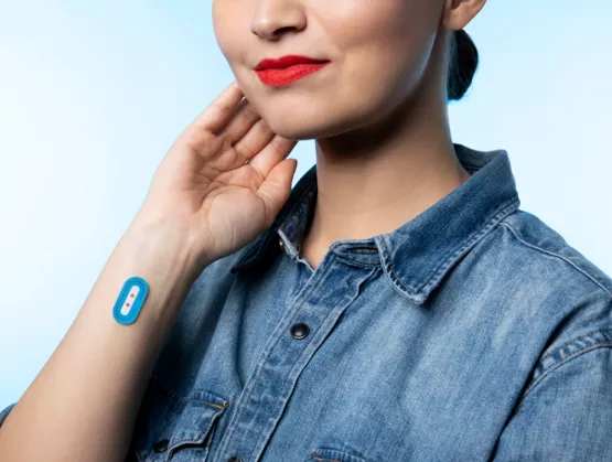
Photo on left: My Skin Track pH by L'Oréal Group’s La Roche-Posay – the first wearable sensor and companion app to easily measure personal skin pH levels – leverages two decades of microfluidic and soft materials research in Professor John Rogers’ laboratory at the Center for Bio-Integrated Electronics and the Simpson Querrey Institute. As director of the Center for Bio-Integrated Electronics at Northwestern University, Professor John A. Rogers explores soft materials for conformal electronics, nanophotonic structures, microfluidic devices and MEMS, all with an emphasis on bio-inspired and bio-integrated technologies. During his keynote at FLEX and MEMS Sensors Technical Congress 2019, February 18-21 in Monterey, Calif., Rogers will present examples of the diverse, novel classes of biocompatible electronic and microfluidic systems with skin-like physical properties that stem from his work in materials science, mechanical engineering, electrical engineering and advanced manufacturing. SEMI’s Maria Vetrano caught up with Rogers to discuss his research, which has already been commercialized by companies such as L'Oréal Group.SEMI: What is the concept behind skin-interfaced electronic and microfluidic devices?ROGERS: Biological systems are mechanically soft, with complex, time-dependent 3D curvilinear shapes. Modern electronic and microfluidic technologies are rigid, with simple, static 2D layouts. We believe that eliminating this profound mismatch in physical properties will create vast opportunities in microsystems technologies (electronics, optoelectronics, microfluidics and microelectromechanical devices) that can intimately integrate with the human body for diagnostic, therapeutic or surgical functions. Skin-like devices that assess blood-glucose levels in real-time or continuously monitor the vital signs of infants in neonatal intensive care are just two examples of non-invasive, wirelessly connected biocompatible devices with the potential to dramatically improve quality of life.SEMI: What are some examples of commercially available biocompatible/microfluidic wearables that have leveraged your research?ROGERS: We’ve been fortunate in that we have been able to translate some of our ideas into commercial products for broad deployment in both life-enhancing and potentially life-saving applications. In sports and fitness, our skin-interfaced microfluidic systems form the basis of soft devices that capture, store and perform in-situ chemical analysis of sweat. These devices have been launched as products in two different categories – cosmetics and athletics – with two global brands. As an example of the former, L’Oréal Group just unveiled at CES 2019 My Skin Track pH, a thin, flexible version of this technology, designed to determine skin pH from measurement of sweat pH. Once armed with this information, L’Oréal customers can choose skincare products matched to their personal body chemistry. See the video on this device. Notably, a globally recognized consumer brand will reveal a product for athletics around the time of the 2019 Super Bowl on Sunday, February 3. A look inside My Skin Track pH, which uses Rogers Research Group technology from the Center for Bio-Integrated Electronics at Northwestern University Our technologies also have applications in clinical medicine and rehabilitation, including soft, skin-interfaced wireless sensors used to assess patient progress in stroke rehabilitation. In contrast with conventional, wired sensors that tether the patient to external boxes of electronics (a design that makes such devices impractical for in-home use), or conventional wearables that are confined to the wrist, our systems apply to the skin like a BAND-AID, and are described as “imperceptible” by stroke patients who are using them during rehab. These platforms measure speech, swallowing capability, movement of limbs, sleep quality, walking and balancing. Healthcare professionals can use the information collected to continue to monitor patients when they leave medical facilities, to understand how patients function in the real world. See video.SEMI: What work are you doing beyond flexible devices?ROGERS: We are pursuing devices that are unique not due to their soft mechanics, but due to their extremely small sizes. A good example is My Skin Track UV, which we recently commercialized with L’Oréal’s La Roche-Posay. This millimeter-scale, wireless, battery-free platform for digital UV dosimetry measures UV exposure dose continuously in real time and provides user access to this information via a smartphone app. My Skin Track UV is now available at all Apple stores across the U.S. and through the Apple website. See video. L’Oréal’s La Roche-Posay My Skin Track UVOther biocompatible/microfluidic devices based on our technology provide functionality that can save lives. Hydrocephalus patients suffer from a condition that, if unchecked, leads to excessive buildup of fluid in the brain. If left untreated, the resulting pressures can prove fatal.Hydrocephalus is treated with shunts, which drain accumulated fluid away from the intracranial space to a distal part of the body, often the abdomen. Unfortunately, however, shunts have a nearly 100 percent fail rate over a 10-year period, and testing them typically requires an MRI, CT scan or even surgery. Our technology serves as the basis of a bandage-sized, skin-like sensor that applies to the surface of the skin on the neck. Within five minutes of placement on the skin, the sensor can test non-invasively to determine if fluid is flowing through the shunt. The net result uniquely supports the rapid evaluation of shunts from home or other non-medical settings. The devices free patients from the constraints of hospitals, giving them a greater sense of security and independence. See video. SEMI: What would you like FLEX and MSTC attendees to take away from your presentation?ROGERS: I would like attendees to know that biocompatible microfluidic and electronic wearables that are flexible and conformal to the human body are no longer risky futuristic technologies that exist only in academic labs: They are emerging right now as key products in commercial markets for flexible hybrid electronics (FHE) and MEMS/sensors. Our group alone is anticipating deployment at the scale of tens to hundreds of millions of units in the markets in which we are seeing traction over the next five years. We believe that the broader area will become a multi-billion-dollar market opportunity in five to 10 years.John Rogers, Ph.D. will present Soft Electronic and Microfluidic Systems for the Skin at FLEX/MSTC on Tuesday, February 19 at 10:30 am.Register today to connect with him at the event. To learn more about Rogers Research Group, click here.MSTC Flex 2019 is organized by the MEMS Sensors Industry Group (MSIG) and FlexTech.Maria Vetrano is a public relations consultant at SEMI.
Read More
Marcellino Gemelli, director of global business development at Bosch Sensortec, will present at the upcoming MEMS Sensors Executive Congress on October 29-30, 2018 in Napa, Calif. SEMI’s Maria Vetrano caught up with Gemelli to give MSEC attendees a preview of Gemelli’s feature presentation.Sensor fusion — the integration of different types of sensors through software algorithms to increase overall system performance and/or reduce power consumption— has come a long way since its inception. In those early days, sensor fusion generally involved MEMS inertial sensors only. The advent of new sensor varieties, including environmental sensors, is making new use cases a reality. Gemelli will explore the ways in which the next generation of sensor fusion is improving autonomous mobility devices. SEMI: Why are environmental sensors important to autonomous mobility devices?Gemelli: When most of us think of autonomous systems, we think that they are driven by motion sensors and proximity sensors (e.g., radar, Lidar). When vertical location comes into play, however, in applications such as drones or asset tracking, pressure sensors become an integral part of flight control, navigation and positioning in GPS-challenged areas.While not commonly considered an electronically enabled sense, the ability to “smell” the environment opens new opportunities. The quality of a user’s experience with personal cleaning robots and robo-taxis are good examples of where we might want to enable scent detection.SEMI: I’ve never thought much about using sensors to detect smell. How would a robo-taxi or a cleaning robot benefit from scent detection?Gemelli: Fully autonomous cars will inevitably give rise to robo-taxis. In fact, last month Volvo announced its fully electric robo-taxi, and in March 2018 Waymo announced that Jaguar Land Rover’s SUV would join Fiat Chrysler’s Chrysler Pacifica minivans in its planned fleet of robo-taxis, so we may see robo-taxis in the U.S. within the next five years.With robo-taxis fast-approaching, we need technologies that provide the same level of oversight that a taxi driver once fulfilled. Gas sensors would function like an electronic nose (e-nose) in a robo-taxi to inform the taxi’s owner of prohibited passenger behavior, such as eating, drinking or smoking in the vehicle, which could potentially damage the vehicle’s interior. Camera sensors could record the act as proof of the offense.Cleaning robots would be more sophisticated than they are today. In addition to leveraging image and range-finding sensors to more accurately map the rooms in your house, they could also detect scents from spilled red wine, pet urine or other foreign materials. When the cleaning robot, such as a vacuum, detects the foreign substance, it would navigate around the substance instead of going through it and spreading it all over the carpet.In addition to robo-taxis and cleaning robots, I will also discuss asset tracking and drones.SEMI: What role does sensor fusion play in autonomous mobility devices?Gemelli: Combining sensor fusion with artificial intelligence (AI) will generate new use cases and therefore new markets for sensor suppliers.There is another major benefit as well. With so many connected devices in our lives — including those with cameras, location awareness and always-listening capabilities — we are seeing growing concern about user privacy. Sensor fusion and AI can help to alleviate this concern: By supporting more local processing, they allow for greater control of data, safeguarding personal privacy.SEMI: Who is responsible for the AI part of the sensor-fusion equation?Gemelli: AI is a new frontier for MEMS and sensors suppliers. It benefits us and our customers to embrace AI algorithms through in-house development and/or partnerships.SEMI: What would you like MEMS Sensors Executive Congress attendees to take away from your presentation?Gemelli: I plan to issue a call to action to increase research in hybrid sensor-fusion software architectures, including AI, as suppliers’ collaboration will benefit the industry at large.Marcellino Gemelli is currently based in Palo Alto (CA) responsible for business development of Bosch Sensortec's MEMS product portfolio. He received the ‘Laurea’ degree in Electronic Engineering at the University of Pavia, Italy while in the Italian Army and an MBA from MIP, the Milano (Italy) Polytechnic business school. He previously held various engineering and product management positions at STMicroelectronics from 1995 to 2011 in the fields of MEMS, electronic design automation and data storage. He was contract professor for the Microelectronics course at the Milano (Italy) Polytechnic from 2000 to 2002.Marcellino Gemelli will present Environmental Sensors Systems Enabling Autonomous Mobility on Tuesday, October 30 at MEMS Sensors Executive Congress in Napa Valley, Calif.Register today to learn more about the connection between sensor fusion, AI and next-generation autonomous mobility devices.Maria Vetrano is a public relations consultant at SEMI.
Read More
SEMI met with Heinz Martin Esser, managing director at Fabmatics GmbH, to discuss how existing 200mm semiconductor fabs can master the challenges of a 24x7 production under highest cost and quality pressure by implementing intralogistics automation solutions. The two spoke ahead to his presentation at the Fab Management Forum at SEMICON Europa 2018, 13-16, November 2018, in Munich, Germany. To register for the event, click here. SEMI: Looking at the latest production capacity data for 2018 – it is a 200mm fab boom. Growing demand for analog, MEMS and RF chips continues to cause acute shortages for both 200mm fab capacity and equipment. Do you think this trend will continue the next years or is it only a short term run on 200mm fabs?Esser: We at Fabmatics believe in a long-term trend. The emergence of the Internet of Things and growing digitalization in all areas of life will continue to increase demand for integrated circuits (ASICs), analog ICs, high-performance components and micro-mechanical sensors (MEMS) in the coming years. Many of these semiconductor elements should be produced in 200 mm fabs.SEMI: How does Fab automation contribute to increase capacity of existing, mature 200mm fabs?Esser: We are convinced that fab automation is one of the greatest potentials for older 200mm factories to effectively master increased demand, increasing efficiency, quality assurance and flexibility at the same time. In particular, material flow automation, which is often the missing link between existing equipment in different production areas, can help increase productivity in an elementary way.If you analyze how long valuable tools typically wait for loading and unloading, you can see a direct effect of the intralogistics automation system, which leads to a significantly higher utilization of process equipment by making the material flow independent from human performance. Additional side effects such as reduced cycle time, stable fab flow factor or flattened WIP shafts further increase the contribution of material flow automation to get the most out of existing mature factories. Older does not mean obsolete.SEMI: What are the biggest challenges for a successful implementation?Esser: There is no single challenge when you automate an existing mature fab. Instead, you face a whole variety of challenges you have to tackle, ranging from historically grown non-aligned fab layouts over non-linear material flows and older non-standardized equipment to “automation unfriendly” fab environment. Also you should not underestimate the efforts to overcome the practice manual fab operation people in the cleanroom are so familiar with for many years. Before doing automation you have to think automation, i.e. you have to question all processes to make them ready for automation.SEMI: What are the key drivers to automate a mature fab today: costs, process stability, quality or a combination of them?Esser: This question should be better asked to our customers, but we believe it is a mix of many impacts. Most likely everybody sees the cost reduction at first, but we get more aware of process and performance stability as well as quality requirements – and here our customers’ play the most important role – become more and more focused.SEMI: What do you expect from SEMICON Europa 2018 and why do you recommend attending the Fab Management Forum?Esser: This year SEMICON Europa will co-locate with electronica. So it`s going to be the greatest trade fair for electronics manufacturing in Europe. We will meet innovators and decision-makers across the whole electronics supply chain. The Fab Management Forum addresses a highly topical question that concerns all semiconductor manufacturers not only in Europe - how to handle complexity and enable the necessary flexibility to cope with customers' needs. High-ranking speakers will give an insight into the latest technologies and best practices. I am looking forward to the lively exchange with the participants and taking away new impulses for our business. Heinz Martin Esser is managing director at Fabmatics GmbH, responsible for sales and marketing, customer service and administration. He studied supply engineering at the University of Applied Sciences in Cologne and later earned a university degree in business administration. Serena Brischetto is a marketing and communications manager at SEMI Europe.
Read More
2017 was a good year for the MEMS and sensors business, and that upward trend should continue. We forecast extended strong growth for the sensors and actuators market, reaching more than $100 billion in 2023 for a total of 185 billion units. Optical sensors, especially CMOS image sensors, will have the lion’s share with almost 40 percent of market value. MEMS will also play an important role in that growth: During 2018–2023, the MEMS market will experience 17.5 percent growth in value and 26.7 percent growth in units, with the consumer market accounting for more than 50 percent(1) share overall. Evolution of SensorsSensors were first developed and used for physical sensing: shock, pressure, then acceleration and rotation. Greater investment in R D spurred MEMS’ expansion from physical sensing to light management (e.g., micromirrors) and then to uncooled infrared sensing (e.g., microbolometers). From sensing light to sensing sound, MEMS microphones formed the next wave of MEMS development. MEMS and sensors are entering a new and exciting phase of evolution as they transcend human perception, progressing toward ultrasonic, infrared and hyperspectral sensing.Sensors can help us to compensate when our physical or emotional sensing is limited in some way. Higher-performance MEMS microphones are already helping the hearing-impaired. Researchers at Arizona State University are among those developing cochlear implants — featuring piezoelectric MEMS sensors — which may one day restore hearing to those with significant hearing loss. The visually impaired may take heart in knowing that researchers at Stanford University are collaborating on silicon retinal implants. Pixium Vision began clinical trials in humans in 2017 with its silicon retinal implants.It’s not science fiction to think that we will use future generations of sensors for emotion/empathy sensing. Augmenting our reality, such sensing could have many uses, perhaps even aiding the ability of people on the autism spectrum to more easily interpret the emotions of others.Through my years in the MEMS industry, I have identified three distinct eras in MEMS’ evolution: The “detection era” in the very first years, when we used simple sensors to detect a shock. The “measuring era” when sensors could not only sense and detect but also measure (e.g., a rotation). The “global-perception awareness era” when we increasingly use sensors to map the environment. We conduct 3D imaging with Lidar for autonomous vehicles. We monitor air quality using environmental sensors. We recognize gestures using accelerometers and/or ultrasonics. We implement biometry with fingerprint and facial recognition sensors. This is possible thanks to sensor fusion of multiple parameters, together with artificial intelligence. Numerous technological breakthroughs are responsible for this steady stream of advancements: new sensor design, new processes and materials, new integration approaches, new packaging, sensor fusion, and new detection principles.Global Awareness SensingThe era of global awareness sensing is upon us. We can either view global awareness as an extension of human sensing capabilities (e.g., adding infrared imaging to visible) or as beyond-human sensing capabilities (e.g., machines with superior environmental perception, such as Lidar in a robotic vehicle). Think about Professor X in Marvel’s universe, and you can imagine how human perception could evolve in the future! Some companies envisioned global awareness from the start. Movea (now part of TDK InvenSense), for example, began their development with inertial MEMS. Others implemented global awareness by combining optical sensors such as Lidar and night-vision sensors for robotic cars. A third contingent grouped environmental sensors (gas, particle, pressure, temperature) to check air quality. The newest entrant in this group, the particle sensor, could play an especially important role in air-quality sensing, particularly in wearable devices.Driven by increasing societal concern over mounting evidence of global air-quality deterioration, air pollution has become a major topic in our society. Studies show that there is no safe level of particulates. Instead, for every increase in concentration of PM10 or PM2.5 inhalable particles in the air, the lung cancer rate is rising proportionately. Combining a particle sensor with a mapping application in a wearable could allow us to identify the locations of the most polluted urban zones.The Need for Artificial Intelligence To realize global awareness, we also need artificial intelligence (AI), but first, we have challenges to solve. Activity tracking, for example, requires accurate live classification of AI data. Relegating all AI processing to a main processor, however, would consume significant CPU resources, reducing available processing power. Likewise, storing all AI data on the device would push up storage costs. To marry AI with MEMS, we must do the following: Decouple feature processing from the execution of the classification engine to a more powerful external processor. Reduce storage and processing demands by deploying only the features required for accurate activity recognition. Install low-power MEMS sensors that can incorporate data from multiple sensors (sensor fusion) and enable pre-processing for always-on execution. Retrain the model with system-supported data that can accurately identify the user’s activities. There are two ways to add AI and software in mobile and automotive applications. The first is a centralized approach, where sensor data is processed in the auxiliary power unit (APU) that contains the software. The second is a decentralized approach, where the sensor chip is localized in the same package, close to the software and the AI (in the DSP for a CMOS image sensor, for example). Whatever the approach, MEMS and sensors manufacturers need to understand AI, although they are unlikely to gain much value at the sensor-chip level.Heading to an Augmented WorldWe have achieved massive progress in sensor development over the years and are now reaching the point when sensors can mimic or augment most of our perception: vision, hearing, touch, smell and even emotion/empathy as well as some aesthetic senses. We should realize that humans are not the only ones to benefit from these developments. Enhanced perception will also allow robots to help us in our daily lives (through smart transportation, better medical care, contextually aware environments and more). We need to couple smart sensors’ development with AI to further enhance our experiences with the people, places and things in our lives.About the authorWith almost 20 years’ experience in MEMS, sensors and photonics applications, markets, and technology analyses, Dr. Eric Mounier provides in-depth industry insight into current and future trends. As a Principal Analyst, Technology Markets, MEMS Photonics, in the Photonics, Sensing Display Division, he contributes daily to the development of MEMS and photonics activities at Yole Développement (Yole). He is involved with a large collection of market and technology reports, as well as multiple custom consulting projects: business strategy, identification of investment or acquisition targets, due diligence (buy/sell side), market and technology analyses, cost modeling, and technology scouting, etc.Previously, Mounier held R D and marketing positions at CEA Leti (France). He has spoken in numerous international conferences and has authored or co-authored more than 100 papers. Mounier has a Semiconductor Engineering Degree and a PhD in Optoelectronics from the National Polytechnic Institute of Grenoble (France).Mounier is a featured speaker at SEMI-MSIG European MEMS Sensors Summit, September 20, 2018 in Grenoble, France. (1) Source: Status of the MEMS Industry report, Yole Développement, 2018
Read More
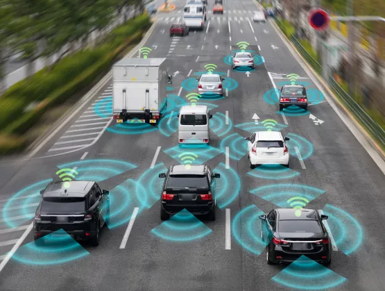
Emboldened by advances in self-driving and Internet of Vehicles (IoV) technologies, Taiwan’s microelectronics sector is investing heavily in manufacturing processes and equipment as engines of innovation and growth for autonomous driving, the world’s next market goldmine. But breaking into the self-driving vehicle industry can be a steep uphill climb. Semiconductor players hungry to secure their piece of the potentially massive market must know how to navigate the automotive industry’s unique ecosystem of suppliers, not to mention its lofty standards for safety and reliability.To explore opportunities and challenges in the automotive semiconductor market, SEMI recently organized Mobility Tech Talk – a gathering of experts from Strategy Analysis, Yole Développement, Renesas, X-FAB and IHS Markit who examined the evolution of sensors for autonomous cars, advanced driver-assisted system (ADAS) applications, and new energy vehicles (NEVs) in China. Nearly 200 participants exchanged in-depth, forward-looking insights and perspectives as the event helped forge stronger relations among various market segments. Here are four key takeaways from the conference. Lidar: The Hottest Sensing Technology for Smart AutomotiveLidar, mmWave radar, cameras and inertial measurement units (IMUs) are critical sensing devices for autonomous cars. With sensor and high-speed computing technologies maturing at their current pace, some 350,000 self-driving vehicles are expected to hit the road by 2027. But before a single autonomous vehicle takes to the roadways, self-driving technology must become expert at monitoring a vehicle’s environment.That’s where Lidar, the hottest of all sensing technologies and the key to the holy grail of safe self-driving, comes into the picture. Lidar’s versatility supports multiple essential functions such as mapping, object detection and object movement. The problem is that mass production is still impossible due to the technology's high costs. What’s more, technical issues must still be sorted out with solid-state lidar, mechanical lidar and MEMS. Both startups and traditional tier-1 semiconductor manufacturers are aggressively investing in related research and development in hopes of fulfilling lidar's promise and seizing the market opportunity. Smart Automotive Sets New Quality and Safety StandardsAs cars become smarter, so too must silicon. Chips must support vastly more data generated by in-vehicle connectivity, ADAS, electrification, autonomous driving and an array of other functions that rely on advanced automotive electronics components. With demand for smarter silicon surging, Taiwan semiconductor companies are turning to the automotive chip industry for expertise and serving as OEMs for major automakers.Quality and safety for automotive applications is paramount. In-vehicle semiconductors must meet strict requirements for vehicle control, robustness, liability, cost and quality management to meet the automotive specifications necessary to securing certifications. Smart silicon must also pass all AEC-Q liability standards promoted by North America automakers and score “zero defect” for the ISO/TS 16949 Automotive Quality Management System.China’s New Energy Vehicles To Fuel Semiconductor GrowthTo promote NEVs and reduce fuel consumption of cars with internal combustion engines (ICEs), late last year the Chinese government introduced the Measures for the Parallel Administration of the Average Fuel Consumption and New Energy Vehicle Credits of Passenger Vehicle Enterprises. With China the world’s largest market for NEVs, the policy is forcing automakers in Japan, the U.S. and Europe to accelerate moves towards NEVs that, in turn, will fuel growth in the semiconductor and automotive battery industries. NEVs in China are expected to number 2 million by 2020 before more than doubling to 4.9 million by 2025. Today, most cars still run on ICEs as environmentally friendly motor drives are still under development. In unit shipments, motor drives are expected to surpass ICEs by 2025.Cross-field Collaboration is KeyThe rise of smarter, fully autonomous vehicles – a disruptive Car 2.0 – is unlikely to happen overnight. Rapid growth of the global automotive semiconductor market will continue, with safety and powertrain applications driving the strongest chip demand. Meanwhile, automakers are focusing more on innovations from startups and non-traditional suppliers, and some have even started to develop their own IP and solutions. These paradigm industry shifts are diversifying the automotive supply chain into a cross-domain collaborative network of suppliers, pushing the closed, one-way automotive supply chain into lesser relevance. In the near future, rivals and partners may become indistinguishable as traditional turf wars begin to wane. As ADAS and autonomous cars evolve, and the era of electric cars nears, automotive semiconductors are emerging as the engine of growth for the global semiconductor industry. The automotive semiconductor market is expected to grow at a CAGR of 5.8 percent, reaching US$48.78 billion by 2022.For its part, the SEMI Smart Automotive special interest group connects professionals from the microelectronics and automotive industries. The group promotes the semiconductor industry's development of automotive technologies and cross-domain collaboration to help drive autonomous vehicle innovation.
Read More
Artificial intelligence (AI) is making headlines everywhere, offering a range of capabilities, including location and motion awareness — determining whether a user is sitting, walking, running or sleeping. Behind the scenes, AI is capturing volumes of data. Makers of smartphones and fitness and sports trackers, along with application developers, are all clamoring for this data because it helps them analyze real-world user behavior in depth. Manufacturers gain a competitive edge by tapping this intelligence: Using it to improve user engagement, they increase the perceived value of their devices, potentially reducing customer churn. How can consumer-product manufacturers tap the built-in capabilities of MEMS inertial sensors — which are already ubiquitous in end-user devices — to make the most of AI? Machine learningProduct manufacturers can easily build an activity classification engine using commonly available smart sensors and open-source software. Activity trackers, for example, use raw data first collected via the MEMS inertial sensors that are already installed in smartphones, wearables and other consumer products.With the building blocks in place, consumer-product manufacturers can apply machine learning techniques to classify and analyze this data. There are several possible approaches, ranging from logistic regression to deep learning neural networks.One well-documented method used for classifying sequences in AI is Support Vector Machines (SVM). Physical activities, whether walking or playing sports, consist of specific sequential repetitive movements that MEMS sensors gather as data. MEMS sensors make good use of this collected data, which can be easily processed into well-structured models that are classifiable with SVMs.Consumer-product manufacturers have gravitated toward the SVM model since it is easy to use, scale and predict. Using an SVM to set up multiple simultaneous experiments for optimizing classification over diverse, complex real-life datasets is far simpler than with other approaches. An SVM also introduces a wide range of size and performance optimization opportunities for the underlying classifier.Cost impacts of processing, storage and transmissionIn practice, recognizing user activity hinges on accurate live classification of AI data. Therefore, the key to optimizing product cost is to balance transmission, storage and processing costs without compromising classification accuracy.This is not as simple as it sounds. Storing and processing AI data in the cloud would leave users with a substantial data bill. A WiFi, Bluetooth or 4G module would drive up device costs and require uninterrupted internet access, which is not always possible.Relegating all AI processing to the main processor would consume significant CPU resources, reducing available processing power. Likewise, storing all AI data on the device would push up storage costs.Resolving the issuesTo resolve these technology conflicts, we need to do four things to marry the capabilities of AI with MEMS sensors.First, decouple feature processing from the execution of the classification engine to a more powerful external processor. This minimizes the size of the feature processor size while eliminating the need for continuous live data transmission.Next, reduce storage and processing demands by deploying only the features required for accurate activity recognition. In one example created by UC Irvine Machine Learning Repository (UCI), when an AI model was trained using a dataset of activities with 561 features, it identified user activity with an accuracy of 91.84 percent. However, using just the 19 most determinative features, the model still achieved an impressive accuracy of 85.38 percent. Notably, pre-processing alone could not identify these determinative features. Only sensor fusion enabled the data reliability required for accurate classification. Third, install low-power MEMS sensors that can incorporate data from multiple sensors (sensor fusion) and enable pre-processing for always-on execution. A low-power or application-specific MEMS sensor hub can slash the number of CPU cycles that the classification engine needs. The onboard software can then directly generate fused sensor outputs at various sensor data rates to support efficient feature processing.Finally, retrain the model with system-supported data that can accurately identify the user’s activities.Additionally, cutting the data capture rate can reduce the computational and transmission resource requirements to a bare minimum. Typically, a 50 Hz sample rate is adequate for everyday human activities. This may soar, however, to 200 Hz for fast-moving sports. Reducing dynamic data rate selection and processing in this way lowers manufacturing costs while making the product lighter and/or more powerful for the consumer.High efficiency in processing AI data is key to fulfilling its potential, driving down costs and delivering the most value to consumers. MEMS sensors, in combination with sensor fusion and software partitioning, are critical to driving this efficiency. Operating at very low power, MEMS sensors simplify application development while accurately analyzing motion sensor data.Combining AI and MEMS sensors into a symbiotic system promises a new world of undreamt-of opportunities for designers and end users.This blog post is based on an original article that first ran in EDN. It appears here with the permission of the publisher.
Read More