downloadGroupGroupnoun_press release_995423_000000 copyGroupnoun_Feed_96767_000000Group 19noun_pictures_1817522_000000Member company iconResource item iconStore item iconGroup 19Group 19noun_Photo_2085192_000000 Copynoun_presentation_2096081_000000Group 19Group Copy 7noun_webinar_692730_000000Path
Skip to main content
Default Banner Image

MEMS & Sensors Industry Group

John Smee, VP Engineering, Qualcomm Technologies Inc., will share insights on 5G – which is evolving to enable more reliable connectivity with higher performance in and beyond the era of Internet of Things (IoT) – in his keynote at MEMS Sensors Executive Congress, October 22-24, 2019, in Coronado, Calif.SEMI’s Maria Vetrano caught up with John to give MSEC attendees a preview of his talk.SEMI: Why should MEMS and sensors suppliers stand up and take note of the evolution in 5G, particularly 5G NR?Smee: 5G is the unifying fabric that will connect virtually everything around us. 5G New Radio (NR) is the global standard for a unified, more capable 5G wireless air interface. It will deliver significantly faster and more responsive mobile broadband experiences to users. It will also extend mobile technology to connect and redefine a multitude of new industries, including the IoT.As tens of millions of MEMS and sensors are the core components providing intelligence and interactivity to IoT devices, suppliers need to understand the capabilities and efficiencies that 5G will bring to connect the wide range of MEMS and sensors.We should also recognize that we are at the beginning of the 5G era, and 5G technologies will continue to evolve and expand in the coming years to connect new types of devices in increasingly efficient ways.SEMI: What’s special about the upcoming release of 5G NR, 3GPP Rel-16?Smee: While the first 5G NR release, 3GPP Rel-15, focused primarily on enhanced mobile broadband (eMBB), it also established a solid technology foundation for continued evolution in Rel-16 and beyond.With Rel-16, we are seeing 5G NR’s expansion beyond eMBB to address new tiers of IoT services such as industrial IoT (e.g., automation) with ultra-reliable, low-latency communication (URLLC) and cellular vehicle-to-everything (C-V2X) for more advanced use cases, such as autonomous driving. MEMS and sensors are critically important to both types of use cases as they collect the raw information of the physical world, and 5G is the connectivity of these sensors to the network. This makes the technologies inextricably linked.MEMS and sensors are equally integral to the development of more efficient low-complexity massive IoT devices (MIoT) with in-band 5G NR deployments of enhanced machine-type communication (eMTC)/narrowband Internet of Things (NB-IoT) and the use of the new 5G Core Network. In practical terms, devices that enable smart city use cases – such as smart utility monitoring, connected parking meters, and smart street lighting solutions that support 3GPP Rel-16 – are MIoT devices that will delight city administrators and dwellers with their improved coverage and efficiency. SEMI: In addition to low-complexity MIoT devices, what other markets will benefit most from the evolution in 5G NR?Smee: We continue to enhance 5G NR to support the high-performance IoT, including URLLC.URLLC is one of the many new 5G capabilities that wasn’t possible with the previous generation of cellular technologies, such as LTE. Because it delivers services at very high reliability (i.e., 99.9999%) and ultra-low latency (i.e., sub-1ms), URLLC literally opens up new use cases that that only wired communication could serve in the past. Industrial IoT applications that require a mix of high reliability and low latency, such as robotic arm command and control, are foremost among these new URLLC use cases.Another example of IoT taking advantage of URLLC is smart grid, where faults in the electricity distribution network require immediate protection and control to ensure safety and avoid equipment damage.SEMI: How is Qualcomm building on the eMTC/NB-IoT for low-power wide-area IoT (LPWA) – and how will this influence IoT connectivity?Smee: We continue to evolve eMTC/NB-IoT beyond its initial 3GPP release in Rel-13, making these foundational LPWA IoT technologies more capable and efficient as they become the basis for 5G massive IoT.The most significant updates to eMTC/NB-IoT include multi-cast and positioning support in Rel-14 and improved spectral/power efficiencies in Rel-15. Multi-cast can help service providers to deliver firmware updates over the air with greater efficiency, which speeds deployment of new features. Positioning can create new values, which can inform end users where their assets/packages are located, potentially safeguarding assets in transit. Improving spectral/power efficiencies offers more power-efficient transmissions, which takes less toll on battery-operated devices.With Rel-16, we have further optimized eMTC/NB-IoT, which is supported by the new 5G Core Network and is also deployable in 5G spectrum in-band with other 5G NR services.The evolutionary path ahead for eMTC/NB-IoT enables support for an even wider range of 5G massive IoT devices. New enhancements in the pipeline, such as grant-free uplink and multi-hop mesh, will boost efficiency and coverage area that much more.SEMI: Where do mobile broadband devices such as ultra-high-definition (UHD) security cameras fall within Qualcomm’s realization of 5G-NR?Smee: Mobile broadband is at the core of 5G NR. We see it both powering the new generation of 5G smartphones and expanding beyond traditional devices (including always-connected PCs and tablets) to address the needs of high-performance IoT devices such as UHD security cameras.It’s actually an important part of our vision for 5G to have an industrial network that requires all types of 5G connectivity for devices spanning eMBB (e.g., cameras, laptops), URLLC (e.g., machines) and MIoT (e.g., sensors).SEMI: What can the MEMS and sensors industry do to prepare for the 5G wave?Smee: Because 5G can evolve to deliver even better performance and efficiency for connecting sensors in the 5G world, we will see even more widespread adoption of MEMS and sensors into larger numbers of connected applications. MEMS and sensors suppliers, therefore, need to get ready for the 5G wave by preparing to support 5G connectivity in their devices, which will ultimately help to realize the 5G vision of connecting virtually everything in the world around us.John Smee, Ph.D., is vice president of engineering at Qualcomm Technologies Inc., where he is the 5G R D lead responsible for overseeing all 5G research projects, including end-end systems design and advanced RF/HW/SW prototype implementations in Qualcomm’s wireless research and development group. He joined Qualcomm in 2000, holds over 100 U.S. Patents, and has been involved in the design, innovation, and productization of wireless communications systems such as 5G NR, 4G LTE, 3G CDMA, and IEEE 802.11. He also leads Qualcomm’s companywide academic collaboration program across technologies including wireless, semiconductor, multimedia, security and machine learning. John was chosen to participate in the National Academy of Engineering Frontiers of Engineering program and received his Ph.D. in electrical engineering from Princeton University and also holds an M.A. from Princeton and an M.Sc. and B.Sc. from Queen’s University.Smee will present Evolving 5G NR to Connect the Internet of Things on Wednesday, October 23, 2019, at MEMS Sensors Executive Congress, Coronado Island Marriott Resort Spa in Coronado, Calif.Register today to learn how 5G NR will transform the user experience with MEMS- and sensors-enabled devices in IoT, automation and beyond.Interested in engaging with the MEMS and sensors supply chain? MEMS Sensors Industry Group is a SEMI technology community that enables the MEMS and sensors industry to innovate, address common challenges and accelerate business results.Maria Vetrano is a public relations consultant for SEMI.
Read More
Stefano Zanella, Head of Automotive, Industrial and Location Businesses, TDK InvenSense will present at next month’s SEMICON Taiwan (September 18-20, 2019 in Taipei City, Taiwan). SEMI Taiwan’s Emmy Yi spoke with Stefano for a preview of his talk.SEMI: What macro market trends are driving automotive manufacturers to increase the variety and volume of MEMS sensors in cars?Zanella: The car world is changing. Consumers increasingly view car ownership as less desirable, yet the number of miles traveled and of hours spent in a car are rising steadily. At the same time, cars are changing profoundly, and the pace of change is rapid. To thrive in this new world, automakers are becoming transportation enablers and providers.Many vehicles today autonomously interact with humans and the world around them, operate with less or no human control, and are powered by electric batteries. MEMS sensors – which mimic and augment the five human senses – are front and center in these advancements.Unlike other types of sensors – such as cameras, radar and GNSS/GPSS – MEMS gyroscopes are functional in every environment. Gyroscopes, as well as accelerometers, can supplement those other sensors when they are not available and boost the accuracy of their outputs when they are available. Both camera stabilization and dead reckoning when GNSS is unavailable are good examples of the latter. Other prevalent sensors include MEMS microphones, used to capture voice commands, ultrasonic sensors, which can be leveraged for parking and gesture recognition, and fingerprint sensors, which can improve car security.SEMI: How can automakers stay competitive in this changing landscape?Zanella: Automakers can future-proof their relevance in the transportation market in several ways. By embracing consumer migration toward ride-sharing over car ownership, many are transforming from manufacturers to mobility providers. Carmakers that invest in ride-sharing and other modes of transportation (e.g., scooters) can sustain their profitability, even if the number of vehicles sold eventually shrinks or simply doesn’t grow as much as anticipated.Automakers will need to pursue new avenues of product differentiation. Traditionally, automakers have kept performance and aesthetics to themselves by owning the engine and the body design of the car, leaving nearly everything else to suppliers. Autonomous driving and electrification, however, are pushing automakers to own the battery pack and the autonomous driving software stack.While we are just beginning to see standardization in battery packs, automakers are likely to own the autonomous driving stack for many years to come. Automakers that offer cars with highly functional and efficient batteries and driving stacks stand to gain market share.Automotive infotainment systems will become increasingly crucial as autonomous driving turns everyone into a passenger. Audio subsystem providers such as Harman Kardon, Bose, and Bang Olufsen, for example, jockeyed for attention at the most recent Geneva Motor Show, demonstrating sophisticated surround-sound systems that rival premium-quality home audio setups.With more and more consumers using voice interfaces to interact with devices in the home, drivers are less willing to accept spotty accuracy in the car. Hence, automakers are using more higher-performing MEMS microphones to accurately capture voice commands. This will come as a relief to those of us who routinely yell at our steering wheels while using voice command to try to call home. Demand for higher quality infotainment systems has prompted some automotive OEMs to own the entire infotainment system and work directly with sensor and chipmakers, a level of intimacy that gives automakers a chance to tune sensor and chip development to their own needs. This tighter relationship also positions device suppliers to forge more direct links with drivers.SEMI: Which MEMS sensors are particularly important to tomorrow’s automobiles and why?Zanella: For many years the automotive industry has been integrating more electronics into cars to improve safety, advance the driver and passenger experience, and, more recently, power the car. As vehicles rely less on human control, automakers must replace the senses of the driver with something else. That something else is a bunch of sensors, microphones, cameras, radar and LIDAR to replace vision and hearing.Since MEMS sensors such as accelerometers, gyroscopes and pressure sensors are much more robust than other types of sensors to operate in snow, rain and darkness and other imperfect environments, automakers use them to ensure that the vehicle never gets lost when other sensors and/or the GPS/GNSS signal become unavailable in tunnels or urban canyons. Gyros help determine direction, accelerometers velocity and distance driven, and pressure sensors height, such as when taking a fork on a multi-level highway. At the same time, fingerprint sensors, ultrasonic parking sensors, and temperature sensors are improving convenience, safety and security for the car’s occupants. Automakers increasingly use inertial and environmental sensors, MEMS microphones, fingerprint sensors, and vision/imaging sensors to augment or replace the five human senses on which car drivers have relied for over 100 years. Source: TDK InvenSense SEMI: To what degree can MEMS sensors enable automotive security?Zanella: MEMS sensors are used widely to enhance security today. Some of their mechanisms are easy to understand while some are unexpected. For instance, ultrasonic fingerprint sensors can authenticate the driver of a vehicle to prevent car theft or something less onerous, like a teenage driver taking the car out without permission.Accelerometers and gyroscopes can prevent a new type of spoof on keyless entry systems. Imagine that you are very close to your vehicle. Your car senses the remote control in your pocket and automatically opens the doors when you pull the handle. Now suppose that your car is parked on the street, not far from your house. You leave the remote control home, and the car doesn’t sense the proximity of the remote control. Great! No one can enter your car, unless ... a thief has a big signal amplifier that makes your car think that the keyless entry device is next to the car. In this case, what can an automaker do? Add an accelerometer that restricts the keyless device from broadcasting the entry signal unless you are walking to the car with the device on your person.SEMI: What would you like SEMICON Taiwan attendees to take away from your presentation?Zanella: I would like them to embrace the transformations afoot in the automotive market as well as their associated design challenges since, by overcoming these hurdles, they can offer significant societal benefits such as safer and cleaner transportation. At the same time, these transformations mean significant opportunities for semiconductor industry revenue growth. And while design-to-delivery cycles in automotive are longer than in consumer and mobile, the automotive market supports higher-value devices as well as the chance to fold dozens of MEMS sensors into a single model.To paraphrase Lord Kelvin: If you can’t sense it, you can’t manage it. As suppliers of many key technologies that make intelligent transportation possible, the MEMS sensors industry is in an excellent position to help automakers manage the many challenges ahead.Stefano Zanella, Ph.D., is Head of Automotive, Industrial and Location Businesses at TDK InvenSense, where he brings MEMS sensors (including accelerometers, gyroscopes and microphones) and location solutions to the automotive and industrial markets. Zanella holds an MS and a Ph.D. in Electrical Engineering from the University of Padova, Padova, Italy as well as MBAs from both the UC Berkeley Haas School of Business and from Columbia University.He will present MEMS Sensors Enabling the Smart Car Revolution on Wednesday, September 18, 2019, at SEMICON Taiwan at 1F 4F, Taipei Nangang Exhibition Center, Taipei City, Taiwan. Register today and save 20% to learn how MEMS sensors are transforming the human experience with cars.Connect with Stefano Zanella at SEMICON Taiwan or via LinkedIn. You can also get more information on TDK’s automotive solutions and application guides online.Interested in engaging with the MEMS sensors supply chain? SEMI MEMS Sensors Industry Group is a technology community that enables professionals in the MEMS and sensors industry to innovate, address common challenges and accelerate business results.Emmy Yi is a marketing specialist at SEMI Taiwan.
Read More
Every day it seems like a new portable voice-first device is coming to market. From smart speakers small enough to fit in your pocket to tiny wireless earbuds and voice-activated TV remote controls, we are using voice increasingly to play music, select TV shows, turn on the lights or interact with our smart thermostat. While the popularity of voice-first interfaces has spawned massive diversity in device type, as long as these devices are portable, they have one thing in common: They’re battery-powered, and that could be a problem for consumers who are tired of frequently recharging or replacing batteries. Change the Architecture, Reduce the PowerThe issue lies in the traditional hardware architectures of today’s voice-first devices, which are notoriously inefficient when it comes to power consumption. Such devices rely on a “digitize-first” model of processing voice data in which the heaviest power-consumers, like the analog-to-digital converter (ADC) and the digital signal processor (DSP), do all the heavy lifting up front, right at the start of the audio signal chain. They continuously digitize and analyze 100% of the ambient sound data as they search for a wake word, even if speech is not present and the only sound is noise. Because voice is spoken randomly and sporadically, that continuous digitization of sound wastes up to 90% of battery power.To tackle the battery drain in portable voice-first devices, we need look no further than the human brain. Our brain processes sound very efficiently. Imagine that you are outside your house having a conversation with your neighbor. You are able to focus on what your neighbor is saying because your brain can differentiate between sounds that it should send to the deeper brain for speech processing and sounds that it shouldn’t bother processing further (e.g., dog barks, sirens or car traffic). The brain spends minimal energy up front to decide whether it should spend additional energy on processing down the line. In other words, it saves the most power-intensive processing only for the important sounds.We can mimic the brain’s approach to signal processing by enabling a new “analyze-first” architecture for voice-first devices. This analyze-first approach requires ultra-low-power analog processing technology that can differentiate voice from noise before the sound data is digitized. This keeps the higher-power capabilities in a voice-first system, such as the wake-word engine, in a low-power mode when just noise is present. This approach only wakes up the higher-power chips in the system, e.g., the DSP or ADC, when it detects speech. Like our brain, a voice-first system uses an analyze-first architecture to conserve energy most of the time, saving the heavy lifting, i.e., the wake-word listening, for times when speech is present. The analyze-first architectural approach to always-on listening analyzes the analog microphone prior to digitization, saving considerable power in portable voice-first devices that run on battery. This architectural shift to analyze-first is well worth the investment because it reduces the system’s power consumption in a battery-powered voice-first device by up to 10x. That’s the difference between a portable smart speaker that runs for a month on battery instead of a week or smart earbuds that last for a whole day instead of a few hours on a single charge. Longer battery life in portable voice-first devices generates more good will among consumers, creating another key differentiator for manufacturers engaged in the ultra-competitive race for more users.For more information on the analyze-first architectural approach to voice-first devices, please view our video.Tom Doyle is CEO and founder of Aspinity. He brings over 30 years of experience in operational excellence and executive leadership in analog and mixed-signal semiconductor technology to Aspinity. Prior to Aspinity, Tom was group director of Cadence Design Systems’ analog and mixed-signal IC business unit, where he managed the deployment of the company’s technology to the world’s foremost semiconductor companies. Previously, Tom was founder and president of the analog/mixed-signal software firm, Paragon IC solutions, where he was responsible for all operational facets of the company including sales and marketing, global partners/distributors, and engineering teams in the US and Asia. Tom holds a B.S. in Electrical Engineering from West Virginia University and an MBA from California State University, Long Beach. For more information, visit www.aspinity.com. Aspinity is a member of SEMI-MEMS Sensors Industry Group, which connects the MEMS and sensors supply network, allowing members to address common industry challenges and explore new markets.
Read More
According to market research and strategy consulting firm Yole Développement (Yole), the total market size of MEMS, sensors and actuators will double from $48 billion in 2018 to $93 billion in 2024.[i] The consumer market will continue to drive volume, with applications such as smartphones making up for in volume what they lack in average selling price (ASP). Stronger demand in automotive, biomedical/health, industrial, and voice-first applications (such as smart speakers) will support this upward trajectory. With so much growth ahead of us, how will the design and manufacture of MEMS keep pace with industry demand for higher levels of innovation and integration, lower cost and lower power, smaller footprints, and faster design cycles — all while meeting acceptable price points?We turned to a handful of MEMS manufacturing experts from SEMI-MSIG who will join us at SEMICON West 2019, July 9-11 at the Moscone Center in San Francisco, to explore the complexities of keeping pace with market demand for MEMS over the next decade.Address the Design GapMentor GM, ICDS Division Greg Lebsack and SoftMEMS President Mary Ann Maher see tremendous progress in the manufacturing supply chain for MEMS. At the same time, they acknowledge the significant gap that still exists in design capability for creating the billions of interconnected sensors required for future applications. Greg and Mary Ann will dive into the standards, ecosystem requirements and collaborative design solutions that will allow the micro-sensors industry to meet demand for next-generation wearables, Internet of Things (IoT) products and medical devices.Get Collaborative with Greg and Mary Ann: Addressing the Design Gap to Enable Next Generation Sensor-Based Products, SEMICON West, TechTALKS South, Thursday, July 11, 2019, 10:35-11:00 a.m. Register today.Get to a Really Big NumberFrom thousands of sensors and actuators in a single airplane to hundreds in a single car or a piece of factory equipment to the twenty-plus that ship in each of the hundreds of millions of the world’s smartphones, we aren’t even close to reaching the saturation point for these intelligent devices. SPTS Technologies EVP GM David Butler isn’t living on the Spaceship Enterprise (or the Millenium Falcon, come to think of it) when he says that we are going to get to a trillion sensors. It is going to happen. The questions are: how and when?Connect with David: Enabling the Age of a Trillion Sensors, SEMICON West, TechTALKS South, Thursday, July 11, 2019, 11:00-11:25 a.m. Register today.Shift to Automotive-GradeDemand for optical sensing technologies such as LIDAR is shifting sensor manufacturing requirements from consumer- to automotive-grade, with its enhanced lifetimes, temperature cycling and higher performance specifications. To meet demand, manufacturers are turning to wafer-level processing, since it complies with the hermetic sealing and dew-point control required for the more rigorous automotive-grade applications. EV Group Business Development Director Thomas Uhrmann, Ph.D., will provide an overview of the steps for manufacturing optical elements, including integration with CMOS circuitry, as he offers a window into the future of automotive packaging for sensors.Tune in with Thomas: Future Manufacturing Requirements for Automotive and Photonics Sensing, SEMICON West, TechTALKS South, Thursday, July 11, 2019, 11:25-11:50 a.m. Register today. Measure Twice, Cut OnceFaster time-to-market, improved device yield, and greater productivity in high-volume manufacturing are increasingly critical requirements for MEMS manufacturers. When a single manufacturing error can cost hundreds of thousands if not a million or more dollars — as well as months of development time — designers can save both time and cost by employing an integrated approach to MEMS design. Lam Research Sr. Director of Strategic Marketing David Haynes will explain how simulation, verification and process modeling can address MEMS-specific engineering challenges such as multi-physics interactions, process variations, MEMS + IC integration, and MEMS + package interaction. Using the right tools before committing to actual fabrication can make or break a project.Get Conceptual (and Practical) with David: Enabling Better MEMS from Concept to High-Volume Production, SEMICON West, TechTALKS South, Thursday, July 11, 2019, 11:50 a.m.-12:15 p.m. Register today.Navigate a Dynamic Foundry LandscapeWe’re still living in a one product-one process world when it comes to MEMS manufacturing. This makes bringing a new device to market both time-consuming and expensive. These challenges aside, the functional capabilities of MEMS, combined with small-footprint and low-power options, have made MEMS increasingly popular. How are market dynamics in MEMS manufacturing evolving to accommodate both demand for high-volume, lower-cost products such as MEMS microphones as well as high-value, lower-volume products such as biomedical devices, IoT products and industrial sensors? Rogue Valley Microdevices Founder CEO Jessica Gomez will explain how foundry consolidation through acquisition, collaboration with other ecosystem players, and specialization in vertical markets such as biomedical or optical are some of the approaches that are transforming the MEMS foundry landscape.Join the Evolution with Jessica: Consolidation, Collaboration, Specialization: How Will MEMS Fabs Manage Changing Dynamics, TechTALKS Stage South, Thursday, July 11, 2019, 12:15-12:40 p.m. Register today.i“Status of the MEMS Industry report,” Yole Développement (Yole), 2019 Edition.Maria Vetrano is a public relations consultant at SEMI.
Read More
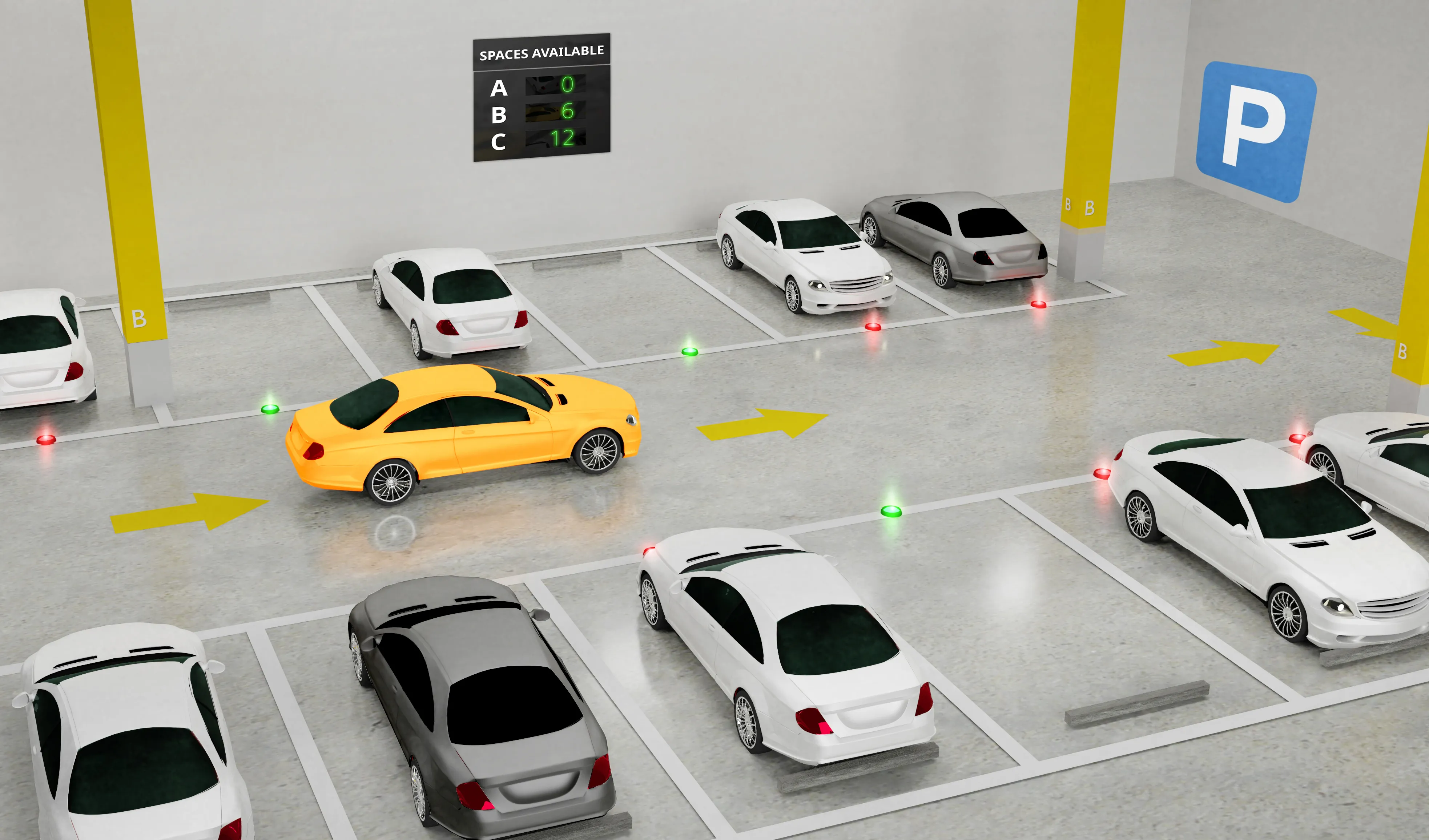
Why Is Smart Parking a Hot Topic? Poorly managed parking resources have a substantial negative impact on cities — one that has been well-documented. According to industry studies, poorly managed parking: Increases Traffic Congestion: 30% of traffic is caused by ongoing circling for parking. Increases Pollution: In Westwood, California, cruising for parking burned 47,000 gallons of gas and generated 730 tons of carbon dioxide in one year. Frustrates Drivers: Urban drivers spend an average of 20 minutes per trip looking for parking. Stifles Economic Opportunities: Traffic congestion cost Americans $124 billion in 2013, and this is predicted to rise to $186 billion by 2030. These problems are getting worse. As a result of growing urban populations, cities account for more than 80% of carbon emissions globally. Unplanned or inadequately managed urban expansion leads to rapid sprawl, pollution and environmental degradation. Due to the lack of parking-space availability, for example, Japan is ranked among the most expensive countries for paid parking. If left unaddressed, poor parking management will continue to plague cities, both large and small. Fortunately, Smart City Internet of Things (IoT) initiatives are helping cities to address their parking issues. IoT to the RescueThere are three key drivers of Smart City IoT initiatives. Cities want to: Improve the overall quality of life and mobility in urban environments Leverage technology to augment and improve existing infrastructure and services that citizens rely on every day Foster both economic and environmental improvements The availability of high-accuracy vehicle detection sensors coupled with affordable, low-power connectivity has enabled a new generation of Smart Parking technology. However, choosing the right Smart Parking solution is essential.High-accuracy vehicle detection sensors can provide valuable data to city planners and parking managers. This information includes: Parking availability Traffic flow Parking occupancy rate and historical data Turnover For parking management to effect change, city traffic managers, parking managers and urban planners need a holistic view of parking availability and usage patterns, and users need real-time information about available parking spaces.Sensors, cameras and communication networks form the basic infrastructure for Smart Parking. To deliver on the promise of IoT and to help cities improve the overall quality of life for residents and visitors, cities need a complete smart parking solution that provides: Accurate real-time vehicle detection and location of available parking spaces – significantly reduces the amount of time spent cruising for parking spaces, giving drivers the precise location of available spaces Connectivity from the sensor to the cloud – facilitates real-time parking data that city planners, parking enforcement and traffic managers can use to reduce traffic congestion Parking applications for cities, parking-lot owners and drivers — enables navigation to available parking and supports mobile payment, streamlining the parking process. Parking applications can also direct traffic enforcement personnel to parking violations as they occur, helping to alleviate traffic bottlenecks, such as double parking in loading zones. Such applications also improve the efficiency of other city services such as public transportation and garbage collection. Complete Smart Parking Solution – Sensor to Cloud (Source: PNI Sensor) To learn how cities are using Smart Parking sensors to improve the services they offer to residents and visitors, come see PNI at SEMI’s 2019 FLEX Japan MEMS Sensors Forum (May 22-23, Toyko, Japan). PNI President and CEO Becky Oh and PNI’s partner, Macnica Networks, will share Smart Parking use cases from innovative cities, corporate campuses and universities (Smart Parking presentation, May 22 from 16:55-17:25). Register for the conference today. For more information about PNI Sensor, visit the PNI Sensor website. Becky Oh is the president and CEO of PNI Sensor. Throughout her 20 years with the company, Ms. Oh has held a range of senior-level positions, from operations to technical business development. She received an M.S. degree in Electrical Engineering from Cornell University and a B.S. in Electrical Engineering and Computer Science from MIT. Ms. Oh holds multiple patents in the area of devices with multi-sensing and reporting capabilities.
Read More
Air pollution is one of the grand challenges facing the entire planet — from the wealthiest nations to the least developed. The World Health Organization reports that nine out of 10 people breathe air containing high levels of pollutants, and that polluted air takes over seven million lives annually through stroke, heart disease and respiratory ailments.As a result, the world is thirsty for reliable, high-performing chemical and environmental sensors that can provide previously unavailable real-time awareness of environmental conditions. On one level, this seems like a relatively simple step, given that smartphones are already equipped with miniaturized sensing technologies that can monitor our living environment and activities.While highly desirable, embedding air pollution sensors in common mobile and wearable devices has not been feasible previously because the necessary trade-offs between high performance and miniaturization have made it impossible.This situation drove a CEA-Leti team to develop a novel generation of fully integrated optical chemical sensors that leverage MEMS technologies. The team successfully merged multiple functionalities on the same chip, using integrated optics and photonics, fluidics, acoustics and electromechanical transduction. How did the team overcome significant technical obstacles to design a proof-of-concept device that senses multiple environmental pollutants — housed in a minimal hardware footprint?Advancing Chemical Sensor Capabilities with Silicon Featuring high selectivity, real-time performance, and fully reversible capabilities, optical chemical sensors are perfect candidates for industrial, environmental and biomedical applications. Consequently, in recent years, worldwide R D initiatives have invested substantial effort to improve them.R D programs have focused particularly on the mid-infrared (Mid-IR) wavelength range (2.5 - 12 µm) — also known as the molecule fingerprint region, which provides a unique combination of fundamental absorption order-of-magnitude bands and unambiguous identification of specific chemicals. A multitude of molecules generate strong and distinct absorption lines in the Mid-IR, providing a foundation for accurate spectroscopic detection. Traditionally, however, these sensors have required large and expensive lenses for infrared (IR) light, making them too big and costly for resource-constrained wearables and mobile devices.Fortunately, recent advances in integrated silicon photonics and quantum cascade laser (QCL) technologies have spurred investigation of new chemical sensor architectures. Richard Soref, a research professor at the University of Massachusetts Boston’s department of engineering, introduced the extension of Near-IR technology into the longer-wave Mid-IR infrared region in 2006. Soref’s concept showed that highly sensitive and selective gas sensors could be fabricated on planar substrates at low cost by co-integrating silicon MEMS, group IV photonics, and specifically designed III-V hetero-structures.While this approach showed promise, it preceded the widespread availability of most mobile devices and wearables. Foreseeing today’s proliferation of those devices, CEA-Leti developed the different building blocks required to implement these concepts in real devices.A New Concept of Integrated OpticsLeveraging these interesting findings, the institute developed a new combination of integrated optics and multiple sensor functions on a single chip: QCL sources, a photo-acoustic (PA) cell, and a mid-IR photonic integrated circuit (PIC) combiner. Their integration on a planar substrate (Figure 1) helped to achieve higher performance, new capabilities, and higher reliability at lower cost, all in a smaller package (less than a 1 cm3 or smaller than a 1-cent coin) with reduced weight and power consumption (less than 100 mJ per measurement). Figure 1: Fully integrated optical sensor (Courtesy: CEA Leti) This configuration represents a multi-gas-detection enabler. The PIC replaces costly, fragile discrete optics while the PA detector uses a MEMS microphone to replace bulky multi-pass cells.PA spectroscopy is among the most sensitive techniques available for monitoring chemical emissions or detecting gas traces. It relies on excitation of the chemical with a pulsed light source emitting at the absorption wavelengths of such molecules. The relaxation process creates local periodic variations of the temperature, resulting in stationary pressure waves, which high-performance microphones can detect.This new generation of devices, fully fabricated on silicon, shows performance comparable with state-of-the-art systems, with the huge bonus of small size and power efficiency that work well for mobile and wearable electronics. By supporting integration onto common technological platforms, such as on-chip photoacoustic sensors, researchers have successfully realized these miniaturized and cost-effective Mid-IR photonic devices in silicon. Mobile device and wearables manufacturers can now take advantage of manufacturable integrated devices for applications that are highly sensitive to size, performance and cost. Adding gas sensing to mobile devices and wearables is now very feasible.For more information on chemical sensing at CEA-Leti, please visit or contact: http://www.leti-cea.com/cea-tech/leti/englishCEA-Leti is an active member of SEMI-MEMS Sensors Industry Group. The technology research institute, along with Fraunhofer and imec, recently joined SEMI’s family as a Strategic Association Partner under a memorandum of understanding (MOU). Under this agreement, CEA-Leti will work with SEMI to advance technology roadmaps, industry standards and cutting-edge technologies including Internet of Things (IoT), artificial intelligence (AI) and machine learning that enable new capabilities across healthcare, automotive and other electronics manufacturing ecosystems. Sergio Nicoletti has more than 20 years of experience in micro and nanofabrication, including magnetic, superconducting and chemical sensing devices and technologies. Having joined CEA-Leti in 2006 as project manager for optical sensing devices used in chemical detection, Nicoletti is currently business development manager at the institute.Previous positions include research and project management at CNR-IMM (Bologna, Italy) and at Hitachi Global Storage Technologies. Nicoletti was also a visiting scientist at HGST (San Jose, Calif.), where he worked on magnetic recording-head devices.Nicoletti holds more than 20 patents and has more than 70 publications in peer-reviewed journals. In 2016, he was appointed coordinator of the European H2020 project MIRPHAB and is director of the project’s pilot line.Nicoletti received his Ph.D. in physics, with a focus on HTc superconducting devices, from Université Joseph Fourier (Grenoble, France). References“Photoacoustic cell on silicon for mid-infrared QCL-based spectroscopic analysis,” JG Coutard, A Glière, JM Fedeli, O Lartigue, J Skubich, G Aoust, A Teulle, T Strahl, S Nicoletti, M Carras, L Duraffourg. Proceedings Volume 10931, MOEMS and Miniaturized Systems XVIII; 109310V (2019) https://doi.org/10.1117/12.2506514“Miniaturization of mid-IR sensors on Si: challenges and perspectives,” S Nicoletti, JM Fédéli, M Fournier, P Labeye, P Barritault, A Marchant, A Glière, A Teulle, J Coutard, L Duraffourg - Silicon Proceedings Volume 10923, Silicon Photonics XIV; 109230H (2019) https://doi.org/10.1117/12.2506759
Read More
For nearly two decades, Sean Ding, CTO and chief scientist of Alibaba Cloud IoT, has worked in software and algorithm architectures, sensing, semiconductors, systems and cloud computing – all areas that have contributed to the rise of the Internet of Things (IoT). It’s no surprise, then, that Alibaba is leading next-generation innovation for the IoT. Ding will bring his expertise to his role as moderator of Brave New World - MSIG Conference on AI+IoT 2019, a half-day forum March 20, 2019, at SEMICON China in Shanghai, China. Maria Vetrano of SEMI spoke with Ding about technologies key to the IoT era including MEMS, sensors, artificial intelligence (AI), edge gateways and cloud computing. SEMI: MEMS sensors are widely used in IoT devices. What is the relationship between AI and MEMS sensors?DING: While MEMS sensors and AI will increasingly co-reside in end-user devices, I do not recommend adding AI next to the sensor (in the same package). That’s because designers continue to use the ASIC for signal conditioning, so A/D converters are still required. Rather, we should look to edge gateways to carry the majority of the workload, including deep learning, because this reduces system complexity and power consumption.SEMI: Why are smarter sensors shifting data processing and analytics to the edge of IoT devices?DING: Data processing and analytics are very important for IoT devices, but we need to focus on understanding the data, parameter calibration and more. The MEMS sensor industry should leave big data analytics to edge computing and cloud computing because AI requires deep learning, demanding a huge amount of data.The challenge is to find the sweet spot for data processing right next to the sensor element.SEMI: What is China’s evolving role in innovation in MEMS sensors for IoT devices?DING: At present, the MEMS community in China needs to figure out how to innovate instead of copying existing technologies, a low-margin business that will not help to grow the industry. One reason why I am so pleased to see the MSIG Conference on AI+IoT in China is that it will encourage greater creativity in the MEMS community in China, and this will ultimately lead to Chinese companies and R D institutions leading innovation rather than copying it.SEMI: What is the right approach to combining smart MEMS sensors with AI in IoT devices? Why is this important for both domestic Chinese and international markets?DING: Combining data from sensors with cloud-edge computing is the right approach. As sensor companies increasingly provide end-to-end solutions, such as “sensor+ firmware + SaaS + app,” we will realize easier and faster integration of sensors in IoT applications.This is incredibly important because China today is the world’s biggest market for IoT hardware. China has 2,000-plus design houses, 200-plus OEMs and thousands of distributors. That said, we still see a highly fragmented market that will benefit from a faster integration methodology.Faster integration of MEMS sensors and AI/machine learning for IoT hardware will benefit designers in international markets as well.SEMI: What do you hope MISG Conference on AI+IoT attendees will take away from the forum? DING: MEMS sensors are highly fragmented, reflecting the highly fragmented applications in which they play. The MEMS sensors industry should figure out how to provide one-stop-shopping solutions for vertical markets. This will speed the scalability of applications and expedite the growth of sensor production. Sean Ding (柯镇) will moderate Brave New World - MSIG Conference on AI+IoT 2019 at SEMICON China on Wednesday, March 20, 2019, at Kerry Hotel Pudong in Shanghai, China.This conference has been organized by the MEMS Sensors Industry Group (MSIG). Register today to connect with Sean Ding and featured speakers at the event.Speakers at the MSIG Conference on AI+IoT 2019 at SEMICON China include: Welcome and Introduction / 欢迎辞Carmelo Sansone, Director, MEMS Sensors Industry Group (MSIG), a SEMI technology community AI Needs Accurate Data – MEMS Sensors Can Provide It / MEMS传感器为人工智能提供真实数据Andrea Onetti, Group VP of Analog MEMS Group, GM of MEMS Sensor Division, STMicroelectronics Enhanced IoT Edge by Smart Sensors / 智能传感器助力IoT边缘智Bennini Fouad, Regional President Asia Pacific, Bosch Sensortec Horizon AI Processor Solution, Enable Industries in AI Time / 地平线AI芯片解决方案,赋能千万业Carl Zhang 张永谦, General Manager/VP, Smart Chip Solutions Division, Horizon Robotics Inertial Sensors in AI Applications / 运动传感器AI应用案例Ben Lee 李彬 , CEO, mCube Ultra-Low-Power Solutions: an Ecosystem Approach / 超低功耗的生态链解决方案Carlos Mazure, IEEE Fellow, Chairman Executive Director, SOI Industry Consortium High-Integrity, Fault-Tolerant Open Inertial Measurement Platform for AI-based Vehicle Automation / 适用于人工智能车辆自动控制的高集成及容错的惯性测量开放平台Dan Dempsey, Senior Director of Automotive, ACEINNA Maria Vetrano is a public relations consultant at SEMI.
Read More
At the SEMI FLEX 2019 and MEMS Sensors Technical Congress (MSTC) (MSTC) February 18-21 in Monterey, California, I had the pleasure of meeting many old friends and colleagues as well as making some great new acquaintances. With MEMS and sensors still a relatively young industry, I am delighted that our community is thriving. We continue to see double-digit growth rates, there is plenty of innovation, and the technology generates massive amounts of data that gets everyone excited about artificial intelligence, deep and machine learning, and blockchain. Those are all the buzzwords that any tech startup needs for funding these days.While it is hard to single out any one presentation at conferences, I was particularly struck by Nadia Shakoor’s keynote address, “Driving Advances in Crop Breeding and Smart Farm Management.” From Nadia I learned that the world’s largest agriculture sensing platform was a mere 45 minutes south of where I live in Phoenix, Arizona. This is a major embarrassment to admit as I have lived here for almost 30 years, have been involved in MEMS and sensors for a decade, and have a particular passion for the use of sensors in agriculture and food to improve crop yields and food quality, and to reduce food waste. This humongous sensor was hiding in plain sight right under my nose!After Nadia’s keynote, I just had to speak to her at the break. Nadia is the senior research scientist and project director for TERRA-REF at the Danforth Plant Science Center based in St. Louis, Missouri. Nadia’s work employs field-level crop phenomics, the biological study of the set of physical and biochemical traits belonging to a given organism (phenomes). Phenomes are fascinating because they change in response to genetic mutation and environmental influences. The Danforth Plant Science Center and its partners are involved in many phenotyping projects using autonomous vehicles, drones, field scanners, satellite imaging and more.After the FLEX MSTC event, I emailed Nadia to ask if I could visit the field scanner and her partner team at the University of Arizona in Maricopa, Arizona. She kindly introduced me to Maria Newcomb, a plant research scientist at the site, who gave me a good look at this mother of all field scanners: the Transportation Energy Resources from Renewable Agriculture Phenotyping Reference Platform (TERRA-REF). TERRA-REF aims to transform plant breeding by using remote sensing to quantify plant traits such as plant architecture, carbon uptake, tissue chemistry, water use and other features to predict the yield potential and stress resistance of 400+ diverse sorghum lines. The TERRA-REF Field Scanner at the University of Arizona Maricopa Agricultural Center. It’s the largest field crop analytics robot in the world, one that’s critical to the crop research underway at the Donald Danforth Plant Science Center in St. Louis, Missouri. Source: Steve Whalley TERRA-REF’s Lemnatec Field Scanalyzer is the largest field crop analytics robot in the world. This high-throughput phenotyping field-scanning robot has a 30-ton steel gantry that autonomously moves along two 200-meter steel rails that have recently been extended another 170 meters. It continuously images the crops growing below it by using a diverse array of cameras and sensors to observe the field at a dense-collection frequency with high resolution. These sensors include RGB stereo; thermal, chlorophyll fluorescence imaging system; hyperspectral cameras; a 3D laser scanner; and environmental monitors.Plant breeding is currently limited by the speed at which phenotypes can be measured, and the information that can be extracted from these measurements. Current instruments used to quantify plant traits do not scale to the thousands or tens of thousands of individual plants that need to be evaluated in a breeding program. The TERRA-REF field scanner system, on the other hand, uses sensors to scan over one acre of plants, collecting thousands of daily measurements throughout the growing season, and these are used to determine plant phenotypes and inform breeding decisions. TERRA-REF’s advanced sensor technologies include: Hyperspectral (250nm-2500nm) Thermal Infrared 2D and Stereo RGB PSII chlorophyll fluorescence 3D laser Environmental sensors The TERRA-REF field scanner platform features a massive sensor-rich scanner head. Source: Steve Whalley The humongous TERRA-REF field-scanner was certainly a sight to behold, looming like a cargo-ship container crane in the vast flat plains of the Arizona desert landscape. I’ve only scratched the surface of what this enormous sensor platform can accomplish so if you are a MEMS/sensor company interested in agriculture and food production, I encourage you to get more information at terraref.org and pay a visit next time you are in the area.Steve Whalley, CEO, Strategic World Ventures, is a strategic consultant to SEMI-MEMS Sensors Industry Group (MSIG). He also consults with established and emerging semiconductor, MEMS and sensors companies.
Read More
As group vice president of the Analog MEMS Group and general manager of the MEMS Sensor division at STMicroelectronics, Andrea Onetti brings nearly three decades of experience in MEMS, sensors and audio systems to his leadership role at one of the world’s most successful electronics and semiconductor manufacturers. During his keynote at FLEX and MEMS Sensors Technical Congress 2019, February 18-21 in Monterey, Calif., Onetti will address the criticality of sensor accuracy in advancing automotive, industrial and consumer applications. SEMI’s Maria Vetrano spoke with Onetti recently to give FLEX/MSTC attendees a preview of his presentation. SEMI: What are some promising advancements in sensors for autonomous cars? Onetti: The avionics industry is already successfully applying sensors for autonomous operationl. Inertial navigation systems (INS) support the operation of planes during flight, both after takeoff and before landing. Unfortunately, the technology in these navigation systems is expensive and not scalable, and they are hampered by reliability limitations in an automotive environment.Following the steady progress that we have made with MEMS inertial sensors in consumer applications, we are on the cusp of realizing greater accuracy in temperature and time – finally delivering the performance required for autonomous driving. Because we can scale in production – we’re now manufacturing more than a billion units a year – we can select the cream of this production crop for adoption in cars. Consequently, we should see Level 3 and Level 4 autonomous driving for consumers very soon.SEMI: How are companies using sensors to monitor and track their assets in industrial applications? Onetti: Predictive maintenance and asset tracking are the two main verticals in Smart Industry. The adoption of multiple sensors for condition monitoring is helping to detect the faulty operation of equipment and to detect early signs of issues that are otherwise difficult to capture. Ultrasonic microphones can detect leaks in a pipe at an early stage, accelerometers with high bandwidth can act as micrometers, and accurate temperature sensors can catch overheating. Similarly, in asset tracking, we use temperature monitoring in combination with inertial sensors to detect problems during the transport of goods. Shock sensors with extremely high full scale (up to 8000g) can tell whether a lightweight envelop has been dropped. Pressure sensors can switch off a radio system when a cargo plane takes off and can mute smart trackers in compliance with flight regulations. We really can do almost anything! A full slate of ST sensors and microcontroller units (MCUs) enable WEG’s small but powerful motor sensor, which listens to a motor, feels its pain, and shares that information with engineers, operators and others to diagnose problems before they happen. Image courtesy of STMicroelectronics. High-accuracy motion, environmental and proximity sensors are crucial to VR/AR. Image courtesy of STMicroelectronics. SEMI: How will sensors advance user experiences in consumer electronics, such as VR/AR systems?Onetti: Virtual reality (VR) and augmented reality (AR) are great examples of promising consumer technologies that will become pervasive as performance of inertial sensors improves. First, we need super accuracy in time and temperature to provide the right experience to users. To achieve this level of accuracy, we need a major step forward in performance, and that includes power consumption and miniaturization. Fortunately, we are constantly making progress in the high-accuracy motion, environmental and proximity sensors that are critical to these systems. While the scale is vastly different between VR/AR and automotive, the requirements for AR/VR systems are pretty similar to those that will enable autonomous cars. A growing variety of sensors (environmental, microphone, proximity, motion) – combined with a sensor hub in an MCU – are central to VR controllers (above) and VR head mounted displays (below). Images courtesy of STMicroelectronics. SEMI: We don’t hear much about the criticality of higher accuracy in sensors. Why is improving accuracy in sensors especially important – and what role do calibration routines play in achieving higher accuracy?Onetti: A sensor is more than just the performance of the relevant function. It is also the intrinsic accuracy that it brings. This accuracy is tuned by calibration, which is typically an expensive process done at the end of product manufacturing or – better still – during earlier stages of manufacturing.Today more applications require sensors with higher accuracy, which necessitates investing more time in calibration, leading to higher cost.MEMS technology can help by offering solutions with intrinsic higher accuracy, which reduces the cost of calibration for product manufacturers. This naturally delivers major benefits to OEMs and, ultimately, their customers.SEMI: What would you like FLEX and MSTC attendees to take away from your presentation?Onetti: As attendees explore the wide variety of available sensor solutions for their end products, I would ask them to prioritize the role of accuracy in sensor selection – because improved accuracy means higher quality data, and higher quality data means better decisions with reduced need for data processing.While designers understand the role of calibration routines in qualifying individual components for specific applications, it is the continuous evolution of MEMS technology that offers the best possibility of breakthrough reductions in time and cost of these calibration routines. This makes MEMS sensors more attractive and affordable than similar sensor components based on different technologies. Andrea Onetti will present Accuracy Enables MEMS Sensor Pervasion at FLEX/MSTC on Tuesday, February 19 at 11:00 am.Register today to connect with him at the event. To learn more about STMicroelectronics, click here. Maria Vetrano is a public relations consultant at SEMI.MSTC FLEX 2019 is organized by MEMS Sensors Industry Group (MSIG) and FlexTech.Maria Vetrano is a public relations consultant at SEMI.
Read More
With over 25 years of experience in the technology industry, Sri Peruvemba, CMO of CLEARink Displays, is a longtime advocate of electronic display technology. During his presentation at FLEX and MEMS Sensors Technical Congress 2019, February 18-21 in Monterey, Calif., Peruvemba will explain recent innovations in electronic paper (ePaper) that will open new applications to reflective displays for the first time. SEMI: ePaper has been around for more than a decade. How has it evolved for wearables and mobile devices?Peruvemba: ePaper in its current form provides a reflective display that is low power and sunlight-readable to applications such as eReaders and electronic shelf labels (ESLs), both of which are in mass production. There is a much larger opportunity, however, for reflective displays that offer color and video atop the traditional benefits of ePaper. Now possible through electrophoretic total internal reflection (eTIR) – which we have termed ePaper 2.0 – is a low-power technology that allows devices to work for days instead of hours. eTIR offers sunlight readability as well as full color and video-level switching speeds, which satisfies the diverse requirements of wearables and mobile devices.New electrophoretic total internal reflection (eTIR) display technology uses the charged particles in a fluid to modulate the total internal reflected light from the optical structures incorporated into its novel reflector film. Image courtesy of CLEARink Displays. SEMI: How do you define a “reflective display?”Peruvemba: A display that reflects external light to its advantage is a reflective display. This includes the display that uses ambient light rather than a backlight and one that uses the sun rather than fights it.SEMI: Where is there a larger opportunity for reflective displays that offer color and video over the traditional benefits of ePaper?Peruvemba: While most of us are familiar with ePaper in applications such as eReaders and wearables that need sunlight readability, there is an untapped market in the wearables space for applications that require internet browsing and color, even video, displays. ESLs are a good example. Retailers are no longer content to show prices. They also want to show specials, display color ads, and run video and animation to enhance product differentiation. Displays in tablets, digital signage and automotive are additional targets.SEMI: How large is the opportunity?Peruvemba: The electronic display industry has been trying to build reflective displays that are low-power color and video for many years but without success. Hence, the opportunity is in the tens of billions of U.S. dollars in outdoor signs, automotive displays, tablets, wearables, shelf labels and dozens of others products.SEMI: What will it take for manufacturers to migrate from LCD or OLED to eTIR?Peruvemba: The good news is that implementation is pretty much the same as with the LCD or OLED displays currently in use. The interfaces, connections and form factors remain form-, fit-, function-compatible. Only the software/waveforms and drive voltages will change/reduce. This allows the manufacture of our tech., ePaper 2.0, on the old LCD lines that are already in use. You can literally go back and forth between ePaper 2.0 and LCD on a day-to-day basis. This differs from other eTIR implementations, which require new dedicated manufacturing lines that cost tens to hundreds of millions of dollars.SEMI: Are there other emerging markets that are particularly well-matched to eTIR?Peruvemba: Tablet devices designed for long use on a single charge, mobile devices including wearables for outdoor applications, Internet of Things (IoT) devices that need high ambient readability, and very low-power and unobtrusive displays in home or office settings represent other emerging markets.SEMI: What technical obstacles have hindered ePaper in certain markets – and how do you overcome those obstacles?Peruvemba: Bringing a display technology to market is not only about solving technical and process hurdles. It is also about finding the right one percent of the applications that your technology can uniquely address. Success requires developing the ecosystem of subcomponent suppliers and peripheral technology providers (like touch and front lights). Partnering with the display fabs that can mass-produce your technology is another important step.With most emerging technologies, the pursuit of the right customer is the bigger challenge, but for us it has been getting the product into production. Fortunately, we already have customers that have invested in the company and have committed to product volume, so they get early access to our technology.SEMI: What would you like FLEX and MSTC attendees to take away from your presentation?Peruvemba: Now just months away from deploying our eTIR technology as ePaper 2.0, we welcome partnership inquiries as we seek to implement eTIR across a range of previously unserved and underserved display markets.Sri Peruvemba will present ePaper 2.0 — Creating New Markets at FLEX/MSTC on Tuesday, February 19 at 2:45 pmRegister today to connect with him at the event. To learn more about CLEARink Displays, click here. MSTC FLEX 2019 is organized by MEMS Sensors Industry Group (MSIG) and FlexTech. Maria Vetrano is a public relations consultant at SEMI.
Read More