downloadGroupGroupnoun_press release_995423_000000 copyGroupnoun_Feed_96767_000000Group 19noun_pictures_1817522_000000Member company iconResource item iconStore item iconGroup 19Group 19noun_Photo_2085192_000000 Copynoun_presentation_2096081_000000Group 19Group Copy 7noun_webinar_692730_000000Path
Skip to main content
Default Banner Image

IoT

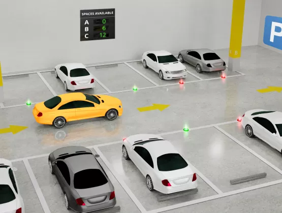
Why Is Smart Parking a Hot Topic? Poorly managed parking resources have a substantial negative impact on cities — one that has been well-documented. According to industry studies, poorly managed parking: Increases Traffic Congestion: 30% of traffic is caused by ongoing circling for parking. Increases Pollution: In Westwood, California, cruising for parking burned 47,000 gallons of gas and generated 730 tons of carbon dioxide in one year. Frustrates Drivers: Urban drivers spend an average of 20 minutes per trip looking for parking. Stifles Economic Opportunities: Traffic congestion cost Americans $124 billion in 2013, and this is predicted to rise to $186 billion by 2030. These problems are getting worse. As a result of growing urban populations, cities account for more than 80% of carbon emissions globally. Unplanned or inadequately managed urban expansion leads to rapid sprawl, pollution and environmental degradation. Due to the lack of parking-space availability, for example, Japan is ranked among the most expensive countries for paid parking. If left unaddressed, poor parking management will continue to plague cities, both large and small. Fortunately, Smart City Internet of Things (IoT) initiatives are helping cities to address their parking issues. IoT to the RescueThere are three key drivers of Smart City IoT initiatives. Cities want to: Improve the overall quality of life and mobility in urban environments Leverage technology to augment and improve existing infrastructure and services that citizens rely on every day Foster both economic and environmental improvements The availability of high-accuracy vehicle detection sensors coupled with affordable, low-power connectivity has enabled a new generation of Smart Parking technology. However, choosing the right Smart Parking solution is essential.High-accuracy vehicle detection sensors can provide valuable data to city planners and parking managers. This information includes: Parking availability Traffic flow Parking occupancy rate and historical data Turnover For parking management to effect change, city traffic managers, parking managers and urban planners need a holistic view of parking availability and usage patterns, and users need real-time information about available parking spaces.Sensors, cameras and communication networks form the basic infrastructure for Smart Parking. To deliver on the promise of IoT and to help cities improve the overall quality of life for residents and visitors, cities need a complete smart parking solution that provides: Accurate real-time vehicle detection and location of available parking spaces – significantly reduces the amount of time spent cruising for parking spaces, giving drivers the precise location of available spaces Connectivity from the sensor to the cloud – facilitates real-time parking data that city planners, parking enforcement and traffic managers can use to reduce traffic congestion Parking applications for cities, parking-lot owners and drivers — enables navigation to available parking and supports mobile payment, streamlining the parking process. Parking applications can also direct traffic enforcement personnel to parking violations as they occur, helping to alleviate traffic bottlenecks, such as double parking in loading zones. Such applications also improve the efficiency of other city services such as public transportation and garbage collection. Complete Smart Parking Solution – Sensor to Cloud (Source: PNI Sensor) To learn how cities are using Smart Parking sensors to improve the services they offer to residents and visitors, come see PNI at SEMI’s 2019 FLEX Japan MEMS Sensors Forum (May 22-23, Toyko, Japan). PNI President and CEO Becky Oh and PNI’s partner, Macnica Networks, will share Smart Parking use cases from innovative cities, corporate campuses and universities (Smart Parking presentation, May 22 from 16:55-17:25). Register for the conference today. For more information about PNI Sensor, visit the PNI Sensor website. Becky Oh is the president and CEO of PNI Sensor. Throughout her 20 years with the company, Ms. Oh has held a range of senior-level positions, from operations to technical business development. She received an M.S. degree in Electrical Engineering from Cornell University and a B.S. in Electrical Engineering and Computer Science from MIT. Ms. Oh holds multiple patents in the area of devices with multi-sensing and reporting capabilities.
Read More
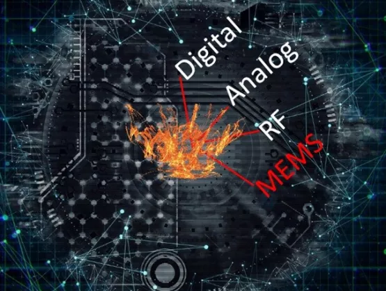
Creating a custom Internet of Things (IoT) IC is challenging because it involves multiple design domains (digital, analog and RF). Creating a sensor-based IC that combines electronics that use the traditional CMOS IC design flow with a MEMS sensor on the same silicon die, however, can seem impossible. Couple the co-design and verification challenges with a lack of traditional process design kit (PDK) support for MEMS, and you have a tough road to travel to get your IoT designs to market.What can we do to make the sensor-based IoT design community successful?Understanding the ChallengesThe sensor-based IoT IC typically features a MEMS sensor (and optional actuator) that interact with the real world. Analog and digital circuitry processes the signals and sends them to a CPU. The CPU provides the “smarts” to process the data from the sensor and then sends processed data via a radio to the Internet; alternatively, the CPU could activate the actuator. A typical sensor-based IoT IC (Source: Mentor: A Siemens Business) Based on the complexity of the system, designers face many co-design challenges: Analog design requirements imposed by MEMS: MEMS devices often require high voltages and multiple power supplies; they emit small signals that need amplification and conditioning; and they are sensitive to the environment and require calibration. Design flow interactions: Parasitics from MEMS devices might affect circuits and vice versa. Circuit designers need MEMS models for impedance and timing. Integration: MEMS devices operate at different timescales than circuits, which adds a layer of complexity. Compounding the problem is a lack of MEMS PDKs and methods to tie together ICs and MEMS PDKs for integration and cross-verification. After conquering the co-design challenges, the design team has to address mixed-domain simulation challenges that include: Simulating the system: This requires verification of MEMS, digital, analog and RF circuitry with embedded software that runs on the CPU. Timescales: These vary widely, from a single deflection of the MEMS transducer in femtoseconds to a seconds-long simulation of the embedded software performing a measurement and transmitting data. Simulation time: Simulation of a behavioral digital design is extremely fast. However, the system simulation requires stand-in models that incorporate the behavior of the analog and MEMS block to simulate in an acceptable amount of time. The challenge of timescales for co-simulation. (Source: Mentor: A Siemens Business) MEMS is the KeyThe reality is that it’s the MEMS device that adds extra complexity to the sensor-based IC design and verification flow. To amplify the problem, the MEMS manufacturing process is not nearly as mature as the standardized IC process. For example, the standardized IC process includes ready-made PDKs that include everything designers need to move through design and verification flows. Foundries often provide soft and hard IP to quickly build-out design, and EDA tools provide high levels of automation enabled by abstraction and a standardized IC flow. How will MEMS-based design evolve?MEMS-based design must catch up to the standardized IC process. The first step is providing MEMS PDKs that include: Multi-physics domain design rules and material properties Packaging information Wafer and bonding information Fabrication information We must also tackle issues associated with these PDKs, including: Ownership, distribution and maintenance of the PDKs Consensus on the contents of the PDKs Merging of CMOS and MEMS PDKs The industry needs to move toward standardized MEMS manufacturing processes with available PDKs. Companies must provide IP and recommend structured design methods for co-design and verification of ICs that incorporate MEMS. How can EDA help with these flows?The EDA ContributionEDA companies must work with teams in the MEMS IC co-design space, collaborating with MEMS fabricators to help enable PDKs. By incorporating PDK support within their own tools, EDA companies can provide an integrated custom IC flow that allows teams to design and verify MEMS-based ICs. For details about this flow, click here to download the Mentor whitepaper: Fusing CMOS IC and MEMS Design for IoT Edge Devices.Greg Lebsack brings 25 years of executive and technical management experience — along with a proven track record of building strong teams and delivering predictable results — to his role as general manager of the ICDS division of Mentor, a Siemens Business. Lebsack joined Mentor in 2015 after that company acquired Tanner EDA, where he was president. Prior to Tanner EDA, he held management and technical positions in a number of different industries and companies, including Sprint, General Electric and McKinsey Co. Greg holds a bachelor’s degree in business administration from Northern Arizona University.Greg Lebsack recently presented on the topic of Integrated Co-design of MEMS/IC at the MEMS Sensors Technical congress, a technical conference organized by the MEMS Sensors Industry Group.
Read More
MedTech, autonomous driving and other disruptive technologies will be in focus at the SEMI Industry Strategy Symposium (ISS Europe), 31 March - 2 April 2019 in Milan, Italy, as top European executives, researchers and academics gather to explore solutions to the region’s most pressing strategic, economic and social challenges. Ahead of ISS Europe, SEMI spoke with Mark Purdy, managing director and chief economist at Accenture Research, about Accenture’s Business Futures – four different future worlds set in 2025 based on the collision of trends across demographics, geopolitics, technology, and economics – and what these futures will mean for markets, workforces, operating models and industry value chains. SEMI: At ISS Europe in Milan, you will kick off the symposium highlighting market opportunities of the digital economy and how companies must adapt to competitive challenges. What inspired Accenture’s Business Futures four world scenarios?Purdy: The impetus for our Business Futures really stemmed from a certain dissatisfaction with current approaches to thinking about the future. We were struck by the following puzzle. First, there is no shortage of techniques for looking at the future, from forecasting to trends analysis to conventional scenarios. Second, most decision-makers have more or less the same access to information on global trends. Yet, time and again, we hear stories of businesses going bust or facing major challenges precisely because they failed to anticipate major changes in their industry.The paradox is that we have so much information, but so little real understanding of how the future actually unfolds. So that set us thinking about how to develop a new approach, based on a combination of detailed trend analysis, expert input and creative storytelling – which is what we call “Business Futures.” SEMI: Of demographics, geopolitics, technology, and economics, which trend do you see as particularly critical?Purdy: Actually, the essence of our Business Futures thinking is that it is the collision or combination of different trends – across economics, technology, demography, etc. – that shapes future outcomes, rather than individual trends per se. To a certain extent we tend to become fixated on specific trends and this can lead us astray or cause bad decision-making. For example, in the early 2000s many people saw very favorable trends in the U.S. economy – strong capital inflows, rapidly rising consumer spending, surging stock markets, and rising home ownership rates. Each trend in isolation looked strong and sustainable. But we failed to see how the combination of these trends was fueling risky financial innovation that would eventually lead to the financial crisis and great recession.Technology of course is a key trend. We are seeing tremendous advances in next-wave technologies such as robotics, machine learning, intelligent objects, 5G and virtualization. But we can only truly understand the impact of the technologies – and the business opportunities and challenges they create – by viewing them against a wider backdrop of changes in society, demography, geopolitics and economics. That is what Business Futures strives to do.SEMI: What will these different futures mean for markets, workforce, operating models and industry value chains?Purdy: There will be profound changes in how we think about all of these areas. Markets will become much more personalized and interactive. Technology will be increasingly integrated with humans, fueling innovation in areas such as personalized healthcare and preventative medicine. Our notions of distance and capacity will be upended, as new virtualized services enable new ways of reaching underserved customers. Consumers will become increasingly involved in the creation and design of products and services. New methods of innovation, powered by AI and virtualization, will come to the fore. New entrants will come from unexpected quarters, enabled by new technology. The upshot will be massive disruption and disintermediation of value chains across many sectors.SEMI: What can Europe do to prepare?Purdy: There are no simple answers, and the correct course will vary by country, but there are some basic things to get right. First, different countries need to understand their comparative advantage – for example, whether it is in services, new technologies, advanced manufacturing or resources – and work with the grain of these different futures. Second, countries need to ensure that they have the basic conditions – regulation, organizational adaptability, workforce flexibility, skills, and innovation infrastructure – to capitalize on the productive potential of new technologies such as AI, virtual reality, and the Internet of Things (IoT). Third, we need to create educational systems and workforce learning methods that emphasize creativity, problem solving and innovation – precisely the skills that will be most needed in an age of intelligent machines. SEMI: What are your expectations for the summit in Milan and for the future?Purdy: I’m very much looking forward to the ISS Europe Summit in Milan. As an economist, I believe we are at a pivotal moment in the semi-conductor industry, driven by waves of technological change and rising geopolitical frictions and uncertainty. With so many industry leaders and experts coming together at the Summit, I’m confident that our discussions will help point a way forward!Mark Purdy is managing director of economic research at Accenture Research. His research examines issues at the intersection of economics, technology and business. He has published widely in tier-1 media and specialised publications on topics such as China’s economy, emerging-market geographic strategy, inclusive economic growth, business futures and the economic impact of new technologies such as the Internet of Things and artificial intelligence. A graduate of Trinity College Dublin, he speaks on these topics at conferences and seminars around the world.Serena Brischetto is a marketing and communications manager at SEMI Europe.
Read More
For nearly two decades, Sean Ding, CTO and chief scientist of Alibaba Cloud IoT, has worked in software and algorithm architectures, sensing, semiconductors, systems and cloud computing – all areas that have contributed to the rise of the Internet of Things (IoT). It’s no surprise, then, that Alibaba is leading next-generation innovation for the IoT. Ding will bring his expertise to his role as moderator of Brave New World - MSIG Conference on AI+IoT 2019, a half-day forum March 20, 2019, at SEMICON China in Shanghai, China. Maria Vetrano of SEMI spoke with Ding about technologies key to the IoT era including MEMS, sensors, artificial intelligence (AI), edge gateways and cloud computing. SEMI: MEMS sensors are widely used in IoT devices. What is the relationship between AI and MEMS sensors?DING: While MEMS sensors and AI will increasingly co-reside in end-user devices, I do not recommend adding AI next to the sensor (in the same package). That’s because designers continue to use the ASIC for signal conditioning, so A/D converters are still required. Rather, we should look to edge gateways to carry the majority of the workload, including deep learning, because this reduces system complexity and power consumption.SEMI: Why are smarter sensors shifting data processing and analytics to the edge of IoT devices?DING: Data processing and analytics are very important for IoT devices, but we need to focus on understanding the data, parameter calibration and more. The MEMS sensor industry should leave big data analytics to edge computing and cloud computing because AI requires deep learning, demanding a huge amount of data.The challenge is to find the sweet spot for data processing right next to the sensor element.SEMI: What is China’s evolving role in innovation in MEMS sensors for IoT devices?DING: At present, the MEMS community in China needs to figure out how to innovate instead of copying existing technologies, a low-margin business that will not help to grow the industry. One reason why I am so pleased to see the MSIG Conference on AI+IoT in China is that it will encourage greater creativity in the MEMS community in China, and this will ultimately lead to Chinese companies and R D institutions leading innovation rather than copying it.SEMI: What is the right approach to combining smart MEMS sensors with AI in IoT devices? Why is this important for both domestic Chinese and international markets?DING: Combining data from sensors with cloud-edge computing is the right approach. As sensor companies increasingly provide end-to-end solutions, such as “sensor+ firmware + SaaS + app,” we will realize easier and faster integration of sensors in IoT applications.This is incredibly important because China today is the world’s biggest market for IoT hardware. China has 2,000-plus design houses, 200-plus OEMs and thousands of distributors. That said, we still see a highly fragmented market that will benefit from a faster integration methodology.Faster integration of MEMS sensors and AI/machine learning for IoT hardware will benefit designers in international markets as well.SEMI: What do you hope MISG Conference on AI+IoT attendees will take away from the forum? DING: MEMS sensors are highly fragmented, reflecting the highly fragmented applications in which they play. The MEMS sensors industry should figure out how to provide one-stop-shopping solutions for vertical markets. This will speed the scalability of applications and expedite the growth of sensor production. Sean Ding (柯镇) will moderate Brave New World - MSIG Conference on AI+IoT 2019 at SEMICON China on Wednesday, March 20, 2019, at Kerry Hotel Pudong in Shanghai, China.This conference has been organized by the MEMS Sensors Industry Group (MSIG). Register today to connect with Sean Ding and featured speakers at the event.Speakers at the MSIG Conference on AI+IoT 2019 at SEMICON China include: Welcome and Introduction / 欢迎辞Carmelo Sansone, Director, MEMS Sensors Industry Group (MSIG), a SEMI technology community AI Needs Accurate Data – MEMS Sensors Can Provide It / MEMS传感器为人工智能提供真实数据Andrea Onetti, Group VP of Analog MEMS Group, GM of MEMS Sensor Division, STMicroelectronics Enhanced IoT Edge by Smart Sensors / 智能传感器助力IoT边缘智Bennini Fouad, Regional President Asia Pacific, Bosch Sensortec Horizon AI Processor Solution, Enable Industries in AI Time / 地平线AI芯片解决方案,赋能千万业Carl Zhang 张永谦, General Manager/VP, Smart Chip Solutions Division, Horizon Robotics Inertial Sensors in AI Applications / 运动传感器AI应用案例Ben Lee 李彬 , CEO, mCube Ultra-Low-Power Solutions: an Ecosystem Approach / 超低功耗的生态链解决方案Carlos Mazure, IEEE Fellow, Chairman Executive Director, SOI Industry Consortium High-Integrity, Fault-Tolerant Open Inertial Measurement Platform for AI-based Vehicle Automation / 适用于人工智能车辆自动控制的高集成及容错的惯性测量开放平台Dan Dempsey, Senior Director of Automotive, ACEINNA Maria Vetrano is a public relations consultant at SEMI.
Read More
New SEMI Taiwan Testing Committee to strengthen the last line of defense to ensure the reliability of advanced semiconductor applications.Mobile, high-performance computing (HPC), automotive, and IoT – the four future growth drivers of semiconductor industry, plus the additional boost from artificial intelligence (AI) and 5G – will spur exponential demand for multi-function and high-performance chips. Today, a 3D IC semiconductor structure is beginning to integrate multiple chips to extend functionality and performance, making heterogeneous integration an irreversible trend. As the number of chips integrated in a single package increases, the structural complexity also rises. Not only will this make identifying chip defects harder, but the compatibility and interconnection between components will also introduce uncertainties that can undermine the reliability of the final ICs. Add to these challenges the need for tight cost control and a faster time to market, and it’s clear that semiconductor testing requires disruptive, innovative change. Traditional final-product testing focusing on finished components is now giving way to wafer- and system-level testing.In addition, the traditional notion of design for testing, an approach that enhances testing controllability and observability, is now coupled with the imperative to test for design, which emphasizes drawing analytics insights from collected test data to help reduce design errors and shorten development cycles. Going forward, the relationship among design, manufacturing, packaging, and testing will no longer be un-directional. Instead, it will be a cycle of continuous improvement.This paradigm shift in semiconductor testing, however, will also create a need for new industry standards and regulations, elevate visibility and security levels for shared data, require the optimization of testing time and costs, and lead to a shortage of testing professionals. Solving all these issues will require a joint effort by the industry and academia. "With leading technologies and $4.7 billion in market value, Taiwan still holds the top spot in global semiconductor testing market," said Terry Tsao, President of SEMI Taiwan. "When testing extends beyond the manufacturing process, it can play a critical role in ensuring quality throughout the entire life cycle from design and manufacturing to system integration while maintaining effective controls on development costs and schedules. Taiwan's semiconductor industry is in dire need of a common testing platform to enable the cross-disciplinary collaboration necessary for technical breakthroughs."The SEMI Taiwan Testing Committee was formed to meet that need, gathering testing experts and academics from MediaTek, Intel, NXP Semiconductors, TSMC, UMC, ASE Technology, SPIL, KYEC, Teradyne, Advantest, FormFactor, MJC, Synopsys, Cadence, Mentor, and National Tsing Hua University to collaborate in building a complete testing ecosystem. The committee addresses common technical challenges faced by the industry and cultivates next-generation testing professionals to enable Taiwan to maintain its global leadership in semiconductor testing.The SEMI Taiwan Testing Platform spans communities, expositions, programs, events, networking, business matching, advocacy, and market and technology insights. For more information about the SEMI Taiwan Testing platform, please contact Elaine Lee ([email protected]) or Ana Li ([email protected]). Emmy Yi is a marketing specialist at SEMI Taiwan.
Read More
4 Key Takeaways from SEMI Taiwan Member ForumThe rapid development of artificial intelligence (AI) has accelerated the digital transformation in various industries and has now fused with Internet of Things (IoT) to exploit the value of both technologies in reshaping the electronics industry value chain. As it emerges from the shadows of its parent technologies, AIoT is giving rise to new opportunities in manufacturing, healthcare, transportation, and even energy. AIoT is fast rising in prominence as an enabler of key electronics manufacturing process improvements and the creation of add-on value to existing products – both critical to the success of many businesses.SEMI and the SEMI MEMS Sensors Industry Group (SEMI-MSIG) held a technical forum on smart sensing and its applications in AI and AIoT, inviting renowned experts in sensors and edge computing to share in-depth insights into the latest AIoT technologies and applications with more than 100 industry professionals in research and development, marketing and sales. Here are four key takeaways from the SEMI Taiwan member forum.1. Steady Growth for Global Sensors MarketThe global sensors market’s steady growth is expected to expand at a CAGR of 6.6 percent from 2017 to 2023, with Asia driving the biggest gains and automotive leading the segments – including healthcare and education – with the strongest growth. Automotive alone is expected to reach US$34 billion in 2023.2. Integration Critical to MEMS Sensors DesignsWith AI booming, MEMS sensor designs need to drive toward greater integration —not only integrating data collection with sensors, but also streamlining data processing on the backend – making 3D models of today’s MEMS mechanical designs critical. The differences between 3D and entrenched 2D models are dramatic, elevating the importance of specifying manufacturing steps in MEMS designs. As new sensors and applications continue to emerge, companies that develop the most powerful integrated designs will win. 3. Growth of Smart Voice-Control Applications to ExplodeAIoT is also accelerating the development of smart voice-control applications and the rise of new related business opportunities. Just 50 million voice-controlled devices shipped worldwide in 2017, a number predicted to swell to 436 million in 2021 with smart home devices such as set-top boxes and smart TVs the major growth drivers.4. AIoT Eyed to Make Human-Robot Collaboration SafeSafety is an essential feature for human-robot collaboration. Tactile sensing technologies give robots a layer of “skin” with capabilities rivaling human touch. To ensure humans and robots work together safely in work environments, sensors on this layer of skin are concentrated – less than 8mm apart, equivalent to the width of a human finger, with a response time of less than 5ms on contact. More than 4 million robots worldwide are expected to be upgraded with these sensing technologies and are on track for deployment in pilot plants in the next three years.SEMI-MSIG is committed to strengthening connections across all sectors in the MEMS and sensors supply chain, working closely with the industry to accelerate the development of related technologies and applications in both mature and emerging markets. In addition, SEMI-MSIG hosts regular events to inspire business opportunities and technology exchange for innovative applications, while enhancing the visibility of members among global customers and partners to help them forge new partnerships. To join the group, contact SEMI Taiwan’s Helen Chen at [email protected] Yi is a marketing specialist at SEMI Taiwan.
Read More
Kyushu, the third largest island in Japan, is home to the semiconductor production bases of integrated device manufacturers (IDMs) with world-class cutting-edge technology. SONY, Toshiba, Hitachi, Mitsubishi, Fujitsu and Nissan are among the sector’s shining stars, though a host of other IDMs tied to the supply chains of other major enterprises have also set root in Kyushu. Collectively, the companies earned Kyushu the name Silicon Island of Japan.Kyushu’s flourishing IDM industry sprouted from favorable tax and other government policies that reduced semiconductor production costs to levels lower than elsewhere in Japan. Once the IC producers had established bases, equipment and materials companies naturally followed, leading to the influx of many parts manufacturers. Together, they came to Kyushu, one after another, to make the island a magnet for manufacturing. And so it was to Kyushu that a SEMI China delegation travelled for a meeting at TEL’s factory in Kumamoto to learn more about the secrets to the rapid growth of the island’s semiconductor industry and promote cooperation between Chinese and Japanese enterprises. Underscoring the rise of the Silicon Island of Japan, China will soon become TEL’s largest market, said Masami Akimoto, Chairman of Tokyo Electron Kyushu Limited, speaking at the event. Masami Akimoto hopes for support from SEMI China.The island of 12 million people contributes to the growth of the global semiconductor industry, expected to reach USD 500 billion in size in 2019 as China’s semiconductor sector, fueled in part by government-backed investment funds, continues its rapid expansion. Despite the gains, China still lags other regions in advanced manufacturing, said Lung Chu, president of SEMI China, which is doing its part to draw more advanced manufacturing to the region through its SIIP platform. The initiative encourages pan-regional cooperation with China’s semiconductor industry to promote free trade, open markets, technology innovation and IP protection – all to help China better integrate with the global semiconductor industry. SEMI China President Lung Chu(L) issues visit memorial to Masami Akimoto(R), Chairman of Tokyo Electron Kyushu Limited. Chicken shall be led by the HenUnlike other regions with comprehensive semiconductor industries, Kyushu’s is primarily focused on production and assembly, with more than 200 manufacturers of semiconductor equipment and parts.SEMI China Delegation at Tokyo Electron Kyushu LimitedTEL built its first factory in Kumamoto, a city covered by volcanic ash in the center of Kyushu, 34 years ago. Today, TEL every month produces 80 to 90 sets of equipment, each consisting of, on average, over 400 thousand parts that must be certified and authorized by TEL before delivery to its module manufacturers and assembly into complete machines. Having blossomed over the past few decades, the island’s supply chain now supplies TEL with all its equipment parts. SEMI China Delegation at Fajita WorksTEL supplier Fajita Works, a high-precision plate metal manufacturer founded in 1945, is emblematic of other companies in the Kyushu supply chain. It keeps a low public profile as it serves several longtime customers and earns ardent loyalty from its workers, an ethos reflected in the change next January of its slog from “Only One” to “Great company, Great life.”Quality is the life of the enterpriseLong before the rise of its legendary automobile and consumer electronics companies, Japan was known for inferior, counterfeited products, labeled “Made In USA” and shipped to the United States by more than 100 factories. The net effect was to shrink and commoditize American markets. The tide in Japan’s product quality and stained reputation began to turn in the 1980s, when Japan’s semiconductor industry began to produce memory with an error rate 27 times lower than its U.S. competitors, giving Japan an upper hand in quality that it would never relinquish. SEMI China Delegation at HORIBAKyushu-based flowmeter supplier HORIBA, among the many Japanese companies famous for their product quality, ships 38 percent of its products into the automotive market and 27 percent into the semiconductor sector. Cleanliness is as vital a part of the company’s culture as quality. Each depends on the other, with fine detail held to the highest importance. On its visit to HORIBA, the SEMI China delegation, passing by an office area before entering the factory, sighed at the sight of the spotless, neatly kept furniture and workspace: They had never seen an office so sparkling clean. HORIBA’s success is rooted in immaculate offices, factories and the company’s motto “Enjoy innovation and pay close attention to product quality.”After Kumamoto sustained heavy damage during a 2016 earthquake, HORIBA workers returned rocks scattered by temblor to their original position, knowing that order is critical to lean, efficient manufacturing and that, indeed, “the devil is in the details.” SEMI China Delegation in Kumamoto City Full confidence in the exploration of Chinese marketConsumer electronics stalwarts Sony and Panasonic feature semiconductor factories in Kagoshima, the southernmost city in Kyushu and Japan, though rumor had it two years ago that Panasonic planned to pull out. The Panasonic plant, which provides batteries for Tesla, remains. The Sony facility produces image sensors for the iPhone.Semiconductor equipment maker ULVAC, SEMI China’s most important strategic partner, is also based in Kagoshima. During the delegation’s visit to the company, Lung Chu noted that while China is the world’s largest semiconductor market, the region meets just 13 percent of domestic chip demand. Stressing that ULVAC can play a crucial role in helping China become a bigger player, he expressed admiration for ULVAC’s professionalism along with hope that it will maintain its rapid growth and leverage SEMI resources to catalyze rapid development of Internet of Things (IoT), artificial intelligence (AI), and 5G technologies in China and rise into the top 10 of global equipment manufacturers. SEMI China President Lung Chu (L) issues visit memorial to ULVAC Kyushu President and CEO Kenji Yamaguchi ULVAC Kyushu president and CEO Kenji Yamaguchi made clear the company’s interest in Lung Chu’s insights into Chinese semiconductor industry while underscoring its core competency of producing semiconductors for flat panel displays. The Kyushu Factory of ULVAC is full of vitality and market competitiveness. SEMI China Delegation at ULVAC EBARA, a precision machinery company located in Kumamoto, has manufactured chemical-mechanical planarization (CMP) equipment for over 20 years and delivered nearly 2,400 mechanical polishing machines worldwide. While the company expects to ship 50 sets per year to China starting next year, it has the capacity to deliver 20 sets per month, enough to meet demand of Chinese semiconductor makers. SEMI China Delegation at EBARAThe most telling takeaway from the SEMI China delegation’s visit to the Kyushu: Japan ranks number one worldwide in research and development (R D) investment as a proportion of GDP and is also at the top in the percentage of R D funds controlled by private enterprises. The outsize investment strategy has enabled Japan to maintain its hold as one of the world’s top technology innovators.Like Sakurajima, the famed Kyushu volcano, the SEMI China delegation will continue to harness its forces to build relationships with the island’s semiconductor supply chain as it works to develop win-win pan-regional relationships and foster the growth of China’s semiconductor industry. Best view of Sakurai volcano Gang Yao is a marketing director at SEMI China.
Read More
Nicolas Sauvage, senior director of Ecosystem at TDK InvenSense, will present at the fast-approaching MEMS Sensors Executive Congress on October 29-30, 2018 in Napa, Calif. SEMI’s Nishita Rao spoke with Sauvage to offer MSEC attendees advance insights on Sauvage’s feature presentation.SEMI: What is “autonomy value” and why is it important?Sauvage: How do you increase the perceived value of an electronic device? If it’s an autonomous car, its value is closely tied to the autonomy level — i.e., the independence — that it offers people. Higher autonomy value for a self-driving car, for example, means that even a blind person could use it. It’s been almost two years since Waymo demonstrated this, and here’s the video that shows it.Countless other sensor-based electronic products have their own “autonomy value.” Imagine the need to get medicine to people during a humanitarian health crisis. Drones could be your best option because they can deliver to inaccessible or remote locations. Unlike older drones, which require active piloting by a person, a drone with higher autonomy value could deliver medicine to Doctors Without Borders without ongoing human intervention.This drone could navigate objects, such as trees and birds, and would have excellent location-awareness. It could fly through any landscape in bright sunlight or during the night. To increase the drone’s autonomy value, you would need better sensors, including those sensors that can enable sensing in sunny conditions or in pitch-black night, as well as better machine learning.SEMI: In this example, what types of sensors would the drone manufacturer need?Sauvage: The manufacturer would need a “surrounding-sensing” solution that includes ultrasonic and pressure sensors as well as image sensors. Start with high-quality image sensors combined with ultrasonic range-finding sensors — high-accuracy devices that function in all lighting conditions and can detect objects of any color. Add motion sensors and a pressure sensor, which would capture the height of the drone to make known the drone’s location in space. The drone would need this combination of sensors, plus smart sensor fusion, because GPS alone cannot avoid obstacles: its signal can be sporadic in certain parts of the world or in certain terrain, making it unreliable.A key attribute of all these sensors would be low power consumption since the drone would run on battery.SEMI: To what extent might autonomy value cause manufacturers to consider multi-vendor solutions?Sauvage: I would like to see it inspire the MEMS and sensors ecosystem to work together, to arrive at multi-vendor solutions that will benefit humanity through greater autonomy value. Whether we’re looking at autonomous cars, drones, robotics or other applications, there are cases where we need to prioritize safety and security over industry competition. SEMI: Where are we today in terms of achieving true autonomy value – and where are we going?Sauvage: The sky is the limit, literally. Machine learning and surrounding-sensing solutions applied to cars, drones and robots will increase autonomy value to the point where we can justifiably call it artificial intelligence.SEMI: What would you like MEMS Sensors Executive Congress attendees to take away from your presentation?Sauvage: I hope that attendees will recognize the value of ecosystem solutions in increasing autonomy value. Together we can expand the variety of sensor types that address novel use-cases and jobs-to-be-done. Instead of waiting for customers to ask for ecosystem-level solutions, we need to articulate a complete MEMS and sensors supply-chain ecosystem if we want the Internet of Things (IoT) and Industrial IoT (IIoT) to grow more quickly. As senior director of Ecosystem, Nicholas Sauvage is responsible for all strategic relationships, including Google and Qualcomm, and other HW/SW/System companies. He is also responsible for strategic and market-driven goal-setting of our SensorStudio developer program, and driving select partnerships with SoC sensor hub platforms. Prior to joining InvenSense, Nicolas was part of NXP Software management team, responsible for worldwide sales, as well as for P L and product management of their OEM Business Line. Nicolas is an alumnus of Institut supérieur d’électronique et du numérique, London Business School and INSEAD. Register today to connect with Nicolas Sauvage at the event. You can also connect with him on LinkedIn.Nishita Rao is a marketing manager at SEMI.
Read More
Cynthia Wright, a retired military officer with over 25 years of experience in national security and cyber strategy and policy, now Principal Cyber Security Engineer at The MITRE Corporation, will give the opening keynote at the upcoming MEMS Sensors Executive Congress, October 29-30, 2018 in Napa, Calif. SEMI’s Maria Vetrano interviewed Wright to give MSEC attendees an advance look at Wright’s highly anticipated presentation.SEMI: MEMS and sensors suppliers provide intelligent sensing and actuation to hundreds of billions of autonomous mobility devices – but historically, our community has not been at the forefront of cybersecurity. Why is now a good time for us to get involved?Wright: From wearables, smartphones, refrigerators and agriculture to medical devices and military hardware, autonomous mobility devices pervade our lives. At the same time, Internet of Things (IoT) botnet attacks like Mirai — and other demonstrated cyberattacks on home devices, vehicles and infrastructure — highlight the increasingly urgent need to address cybersecurity and privacy in MEMS/sensors-enabled devices.As building-block players in autonomous devices, MEMS and sensors suppliers have several good reasons to get involved.The number of IoT cyber security bills before state and federal legislatures suggest that regulation is coming, and it is in everyone’s best interest to prepare. While original equipment manufacturers (OEMs) would generally be held liable in cases of component malfunction or data breach, if insecurity stems from a microelectromechanical component, OEMs would most likely choose component suppliers with secure products.Beyond legislation and competitive advantage, we must consider that people’s well-being, even lives, could be at stake. Imagine what could happen if someone hacks into an insulin pump, the accelerometer on a train, or the LIDAR of an autonomous car. Intrusions of this sort could prove catastrophic.SEMI: Where do you perceive the biggest potential threats to consumers, industry, government?Wright: In good military fashion, I would say that it depends. If a person is a consumer of medical implants, that’s a big threat. On the government side, we could be talking about networked devices involved in military situational awareness. In industry, it could be sensors governing critical manufacturing or safety processes.I am not saying that every sensor must be secure. In every sector, there are areas of greater or lesser vulnerability, depending on context. SEMI: What is security or privacy by design?Wright: Addressing security flaws is cheaper and more easily accomplished at the design stage and not after the vulnerabilities are discovered. At MITRE, we practice systems- and design-oriented thinking as we consult with people doing development. We help them to develop security standards and approaches that are broadly applicable, rather than focusing on a specific product.For example, MITRE looks at the ways that a person might hack into a car to steal location and life history data — or alter its functions — to facilitate general standards and approaches that will help manufacturers better ensure the privacy and security of autonomous vehicles. Hackers have demonstrated that they can interfere with vehicle transmissions and brakes. Ignition, steering and other critical systems are theoretically accessible through the same types of attacks. To what degree can MEMS/sensors suppliers help automotive manufacturers ensure the privacy and security of autonomous cars, and the safety of their drivers? SEMI: What would you like MSEC attendees to take away from your presentation?Wright: MEMS/sensors suppliers are on the leading edge of computing and should take some responsibility for considering cybersecurity and privacy, for the safety of their customers and their own competitive advantage. Recognize which devices should be secure and act accordingly. Get involved at the design stage. The market for secure microelectronics is only going to grow, and this will benefit suppliers who take secure design seriously.Cynthia Wright will present Cyber Security and Privacy in the Age of Autonomous Sensing on Monday, October 29 at MEMS Sensors Executive Congress in Napa, Calif.Register today to connect with her at the event. Maria Vetrano is a public relations consultant at SEMI.
Read More
SEMI met with Heinz Martin Esser, managing director at Fabmatics GmbH, to discuss how existing 200mm semiconductor fabs can master the challenges of a 24x7 production under highest cost and quality pressure by implementing intralogistics automation solutions. The two spoke ahead to his presentation at the Fab Management Forum at SEMICON Europa 2018, 13-16, November 2018, in Munich, Germany. To register for the event, click here. SEMI: Looking at the latest production capacity data for 2018 – it is a 200mm fab boom. Growing demand for analog, MEMS and RF chips continues to cause acute shortages for both 200mm fab capacity and equipment. Do you think this trend will continue the next years or is it only a short term run on 200mm fabs?Esser: We at Fabmatics believe in a long-term trend. The emergence of the Internet of Things and growing digitalization in all areas of life will continue to increase demand for integrated circuits (ASICs), analog ICs, high-performance components and micro-mechanical sensors (MEMS) in the coming years. Many of these semiconductor elements should be produced in 200 mm fabs.SEMI: How does Fab automation contribute to increase capacity of existing, mature 200mm fabs?Esser: We are convinced that fab automation is one of the greatest potentials for older 200mm factories to effectively master increased demand, increasing efficiency, quality assurance and flexibility at the same time. In particular, material flow automation, which is often the missing link between existing equipment in different production areas, can help increase productivity in an elementary way.If you analyze how long valuable tools typically wait for loading and unloading, you can see a direct effect of the intralogistics automation system, which leads to a significantly higher utilization of process equipment by making the material flow independent from human performance. Additional side effects such as reduced cycle time, stable fab flow factor or flattened WIP shafts further increase the contribution of material flow automation to get the most out of existing mature factories. Older does not mean obsolete.SEMI: What are the biggest challenges for a successful implementation?Esser: There is no single challenge when you automate an existing mature fab. Instead, you face a whole variety of challenges you have to tackle, ranging from historically grown non-aligned fab layouts over non-linear material flows and older non-standardized equipment to “automation unfriendly” fab environment. Also you should not underestimate the efforts to overcome the practice manual fab operation people in the cleanroom are so familiar with for many years. Before doing automation you have to think automation, i.e. you have to question all processes to make them ready for automation.SEMI: What are the key drivers to automate a mature fab today: costs, process stability, quality or a combination of them?Esser: This question should be better asked to our customers, but we believe it is a mix of many impacts. Most likely everybody sees the cost reduction at first, but we get more aware of process and performance stability as well as quality requirements – and here our customers’ play the most important role – become more and more focused.SEMI: What do you expect from SEMICON Europa 2018 and why do you recommend attending the Fab Management Forum?Esser: This year SEMICON Europa will co-locate with electronica. So it`s going to be the greatest trade fair for electronics manufacturing in Europe. We will meet innovators and decision-makers across the whole electronics supply chain. The Fab Management Forum addresses a highly topical question that concerns all semiconductor manufacturers not only in Europe - how to handle complexity and enable the necessary flexibility to cope with customers' needs. High-ranking speakers will give an insight into the latest technologies and best practices. I am looking forward to the lively exchange with the participants and taking away new impulses for our business. Heinz Martin Esser is managing director at Fabmatics GmbH, responsible for sales and marketing, customer service and administration. He studied supply engineering at the University of Applied Sciences in Cologne and later earned a university degree in business administration. Serena Brischetto is a marketing and communications manager at SEMI Europe.
Read More