downloadGroupGroupnoun_press release_995423_000000 copyGroupnoun_Feed_96767_000000Group 19noun_pictures_1817522_000000Member company iconResource item iconStore item iconGroup 19Group 19noun_Photo_2085192_000000 Copynoun_presentation_2096081_000000Group 19Group Copy 7noun_webinar_692730_000000Path
Skip to main content
Default Banner Image

IoT

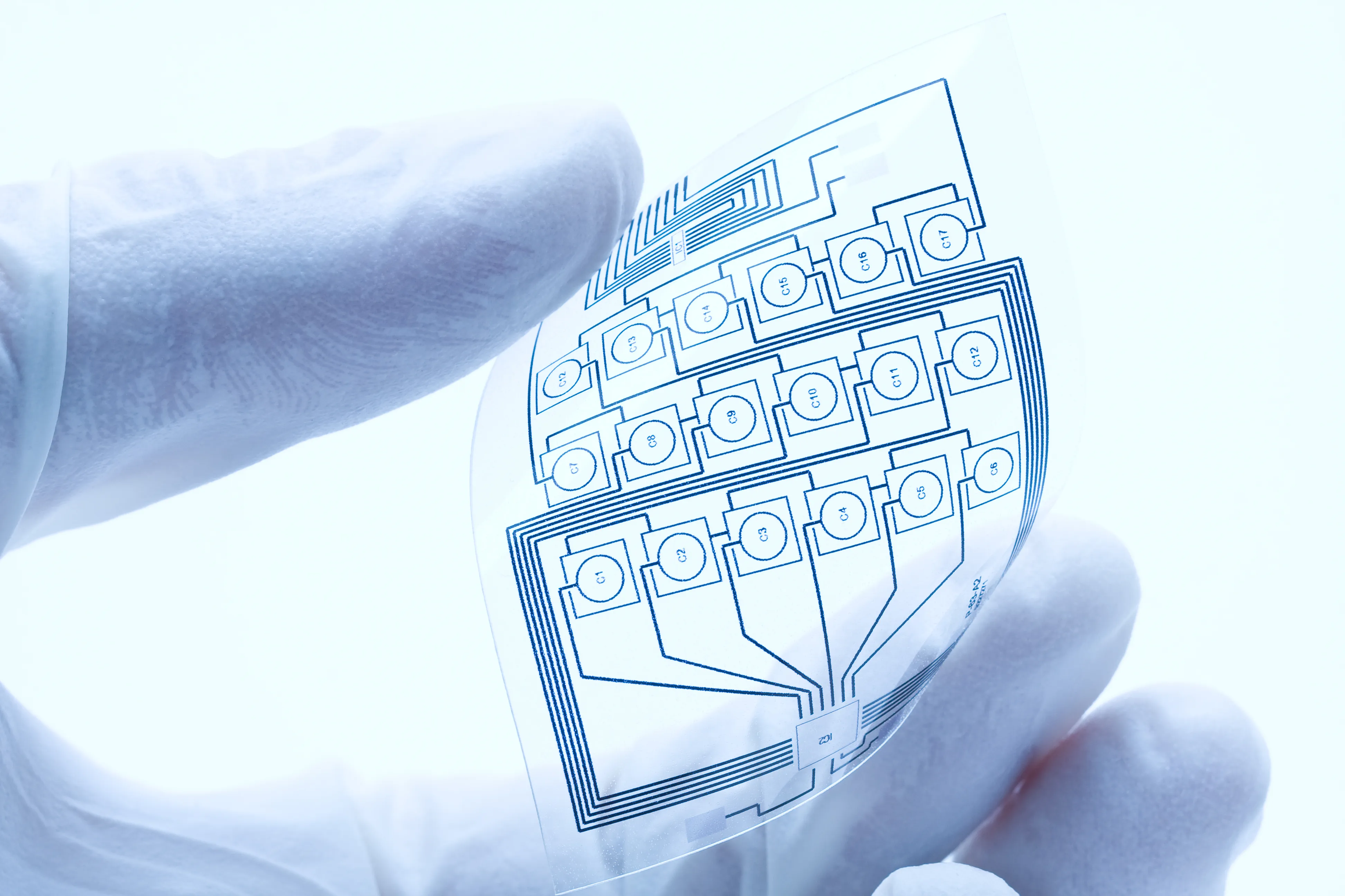
For the first time in its 20-year history, the FLEX Conference dedicated an entire session to the important and timely twin topics of environmental sustainability and power consumption of electronic devices. The event planning committee recognized the urgent need to increase the awareness of how technology and electronics devices can help reduce greenhouse gas emissions (GGE) overall and meet aggressive targets to curb the impacts of climate change. Dr. Christine Ho, CEO of Imprint Energy, delivered the keynote for the session, focusing on the need for powering billions of sensors that will be deployed annually, and their role in reducing fossil fuel emissions through becoming aware of issues, monitoring our resources over time, and intervening early and often to combat waste in multiple sectors and industry. Quoting extensively from the organization Exponential Roadmap Initiative (ERI), Ho noted that “the digital sector has the potential to directly reduce fossil fuel emissions 15% by 2030 and indirectly support a further reduction of 35% by influencing consumer and business decisions and systems transformation.” The initiative’s playbook for reaching net zero carbon emissions by 2050 and limiting global warming to 1.5° Celsius outlines how the digital sector can help remove 13 of the 27 gigatons (GT) of CO2 needed to reach this goal. Ho stated that the rapidly emerging Internet of Things (IoT), devices, software systems, and data insights are the backbone of this digital transformation. The IoT's vast network of sensors can transform multiple sectors, such as the logistics industry, which on an annual basis moves and ships more than 10 billion tons of products worldwide by ships, airplanes, long haul trucks, and train - contributing 17% of GGE and more than 4 gigatons of CO2 annually. Always-connected IoT sensors used by the logistics industry can reduce waste and damage in the supply chain, which is especially problematic for temperature-sensitive and damage prone pharmaceutical and food products, mitigating the need for producing high volumes of buffer inventory to replace damaged goods Noting that the attendees of 20 Years of FLEX Conferences were a big part of the current advancements of low-cost printed, active, shipping tags, Ho said that Imprint Energy’s flexible and thin, Zinc based batteries are ideal for IoT devices, since they boast a significantly smaller carbon footprint than Lithium-Ion (Li-ion) batteries. Imprint Energy is working with systems designers and integrators to design the battery as an integral part of the device package and use low-power strategies to extend device lifetimes. Imprint recommends co-locating battery printing alongside the device integration to further minimize shipping and logistics. When manufactured separately, Imprint’s small footprint, low-operating temperature process line (less than 80°C) provides significant carbon footprint advantages over other technologies. Ho challenged the attendees, saying “we all need to participate in protecting our earth. We need to eliminate waste and contribute to reducing half of our current greenhouse gas emissions by 2030, and we can do that by deploying a global digital skin with more than 100 billion IoT devices in 2030 and up to 1 trillion by 2050. We can minimize the device carbon footprint and maximize its longevity by considering the power capability, as well as design for re-use and re-cycling of the critical materials.” Following Dr. Ho’s presentation, FLEX kicked off a spirited panel discussion with experts from PowerRox, ITN Energy Systems, Birla Carbon, and Auburn University and chaired by Bob Praino and Eric Forsythe, from Chasm Advanced Materials and the Army Research Labs, respectively. The speakers summarized their on-demand presentations and looked at what is being done today to recycle Lithium-Ion batteries, how IoT devices are currently being powered, and drew comparisons between the early days of the Internet and development of the IoT. The speakers generally agreed that the power requirements of wireless cellular and Blue-tooth devices were still too high and run times too short. FLEX 2021 was a virtual event in the 2021 SEMI Technology Series. It was organized by SEMI FlexTech, SEMI NBMC, and NextFlex. Major sponsors included E Ink and Novacentrix. The event covered technical developments in flexible, printed and hybrid electronics, featuring more than 100 presentations and networking opportunities. Technical proceedings are available until March 26 at http://flex.semi.org. Heidi Hoffman is senior director in Corporate Marketing at SEMI.
Read More
SEMI spoke with Eyal Shekel, senior vice president of Service Strategy and Excellence at Tokyo Electron Limited, about the impact of artificial intelligence (AI) on smart manufacturing and how other fab solutions for smarter process tools are advancing semiconductor manufacturing.Eyal shared his views ahead of his presentation at the SEMI Fab Management Forum, 17 February, as part of the SEMI Technology Unites Global Summit, 15-19 February 2021, an online event. Join us to meet experts from Tokyo Electron and other key industry influencers. Registration is open. SEMI: AI technology is considered a key enabler for smart manufacturing. What are the latest trends? Shekel: The advent of advanced nodes and extreme complex 3D semiconductor geometry has lengthened time to market and increased costs in areas ranging from equipment development and large-scale metrology usage to monitoring yield inhibitors.AI is becoming a critical tool in the area of material informatics to determine suitable materials and processing techniques in order to meet the needs of future devices. Together with new materials and processes, the development and implementation of virtual metrology will enable accurate and almost absolute real-time monitoring of our customers’ device wafers at each stage of the manufacturing process.SEMI: What are the benefits of data analysis in the process from R D and Ramp-Up to High-Volume Manufacturing? Shekel: The new research field of materials informatics enabled by AI provides tools to guide the highly efficient discovery and optimization of production processes. For example, TEL has developed methodologies for co-optimizing processes and materials for etch rates.To monitor and manage the yield of semiconductor fabrication processes, direct metrology measurements are important. However, it is difficult to monitor all production wafers due to the time and cost involved. With deep learning AI, it is now becoming possible to predict every wafer’s metrology measurements based on production equipment data and previously processed wafer metrology variables. This enables total quality management and run-to-run control, while simultaneously reducing production costs and cycle time.SEMI: Can you tell us more about TEL Service Advantage?Shekel: TEL Service Advantage is a TEL global support organization that allows customers to select a service plan that fits their needs. Through TEL Service Advantage, we can quickly respond to customer requests and technical advancements. TEL Service Advantage provides various plans to maximize equipment maintenance efficiency for customers and productivity from equipment manufactured by TEL. TEL Service Advantage plans can be combined to meet customer needs and achieve maximum results.A key enabling element of TEL Service Advantage is TELeMetrics™. TEL analyzes equipment data from various sensors using a remote connection and, based on that analysis, provides solutions to customer-specific problems around equipment throughput and predictive maintenance.SEMI: How is AI helping during the pandemic? Can you share a success story? Shekel: The pandemic forced severe travel restrictions worldwide, making it very difficult or even impossible in many cases to visit our customers, as it is still the case today. Standard communication devices like smartphones and email helped at the beginning when TEL intensified the remote support by our Total Support Centre (TSC).TEL continued to develop its Service Advantage program quickly, and started using additional advanced tools and methodologies such as the following: Deployed AR (Augmented Reality) to remotely assist our customer and TEL engineers Secured remote connections into TEL tools to investigate parameters and logs, or to change set-up Used remote training courses that connects trainers via video conferencing systems and training tools in the factories to skill up engineers located in a different parts of the world Used AR glasses for tool start-up and troubleshooting Expanded TEL database global technology with multi-tool on languages search capabilities A key project at a customer site in Europe offers an excellent success story. Using all the approaches above, we collaborated with the local team to put a tool into production with no major delays. This was highly appreciated by the customer and very important for us.SEMI: What do you predict for the future? Shekel: Global technology infrastructure continues to develop and expand rapidly. Elements like 5G networks, IoT and advanced sensing capabilities will lead to what we call General AI, which will be based on neuro-like infrastructure. The auto learning will spread across domains and rely on internal logic and reasoning to automate many tasks that are manual today. In our industry in particular, General AI will enable workers to focus more on data analytics and future advanced R D rather than ongoing operations.SEMI: How can technology unite us? What do you expect from your participation at SEMI Technology Unites Global Summit?Shekel: Technology united us in the last 150 years. The connectivity started with telegraph and telephone and was used to exchange information over wider distances. Nowadays, video conference capabilities, AR and improving communications technology makes it much easier to unite people who are geographically dispersed. This becomes obvious and valuable especially during this pandemic period. As a fact, we are able to continue to perform all our key activities – our tool support, training and customer relationships – even if we cannot be present in person.The SEMI Technology Unites Global Summit is a great chance to stay connected to people and customers that I would normally meet at the SEMICON exhibitions.It also offers the opportunity to network with many more people who I would not be able to meet otherwise. Moreover, I can watch speeches and presentations at any time! Normally I would miss some programs since exhibitions and events took place at the same time.Eyal Shekel, senior vice president of Service Strategy and Excellence at Tokyo Electron Europe Limited, is a 27-year semiconductor industry veteran. Upon his graduation as a Mechanical Engineer from the Technion (Israel leading technical institute), he joined Applied Materials. In 1997 he moved on to Tokyo Electron (TEL) in Europe, served as the Regional Service Manager of Israel and, soon after, was appointed the company’s General Manager. Since 2005 Eyal has been part of TEL Europe senior management. He oversaw the Service and Support Operations for TEL Europe as a senior vice president until 2019. In his current role, he co-leads TEL’s Global Service Committee in Japan.The SEMI SMART Manufacturing Initiative is a global effort to promote awareness of and interest in smart manufacturing with a focus on delivering industry-recognized best-in-class programs and services to enable members to maximize product quality and productivity while reducing costs. Activities are focused on building out core capabilities to enable smart manufacturing across the microelectronics supply chain. MADEin4 is a consortium of 47 partners from 10 countries connecting the full range of supply chain – from semiconductor equipment manufacturers and system-integrating metrology companies to RTOS and key applications such as the automotive industry. The MADEin4 Project develops next generation metrology tools, machine learning methods and applications in support of Industry 4.0 high-volume manufacturing in the semiconductor manufacturing industry. Serena Brischetto is senior manager of Marketing and Communications at SEMI Europe.
Read More
Electric mobility, renewable energy and other technology innovations like IoT, 5G, smart manufacturing and robotics all require reliability, efficiency, and compact power systems, fueling the adoption of Silicon Carbide (SiC) and Gallium Nitride (GaN) to support lower voltages in significantly smaller devices. But chip designers must overcome the technological and economical challenges of integrating the two semiconductor materials into power systems.SEMI spoke with Elisabeth Brandl, Business Development Manager at EV Group about trends and new developments within the power electronics industry and the devices' application in smart mobility. Brandl shared her views ahead of her presentation at the SEMI SMART Mobility Forum, 18 February, as part of the SEMI Technology Unites Global Summit, 15-19 February 2021, online event. Join us to meet experts from EV Group and other key industry influencers. Registration is open. SEMI: What is driving new developments in power electronics?Brandl: Globally there are significant changes in infrastructure requirements for communication, automotive and power conversion. We need to look no further than the rising adoption of 5G, electric and hybrid vehicles, and renewable energy as examples of drivers of these changes. The device level, particularly in the field of power electronics, figures prominently in these shifts.The power electronics industry faces a growing number of scenarios where conventional silicon power devices are no longer suitable and are easily outperformed by new architectures mainly based on wide bandgap semiconductor materials like Silicon Carbide (SiC) and Gallium Nitride (GaN).SEMI: What industry challenges is power electronics innovation aiming to solve? Brandl: Power conversion efficiency is very important and needs further improvement as the related losses significantly contribute to the overall power consumption. For green power and a better environmental footprint, renewable energy is crucial, but so is overall power-consumption efficiency, yet the role of power devices is often underestimated. High-frequency and high-power applications, such as data center applications and inverters for renewable energy, where silicon power electronics are reaching their limits, are also important areas in power electronics.SEMI: How will the transition from silicon to compound semiconductor materials help?Brandl: The superior material properties of several compound semiconductors can tackle the need for lower losses in power conversion or better high-frequency behavior. Today, we mainly talk about GaN and SiC power devices as they are materials well-suited to address these needs. However, other materials like diamond and gallium oxide are in development for these applications. Material properties of SiC that enable thinner materials with lower power losses and better thermal behavior address power conversion efficiency as well as form factor challenges. GaN, especially in a high electron mobility transistor (HEMT), can be used for high-frequency applications.SEMI: What enables a better and more cost-effective manufacturability of SiC and GaN power devices?Brandl: For the end customer, a typical figure of merit regarding the cost effectiveness is $ per Ampere or Watt. While this seems simple, the reality is of course more complex. It is important to understand the main cost contributors within the manufacturing area. For SiC, this is clearly the substrate cost. In my presentation, I will show a way to reduce this cost via wafer bonding. For GaN, epitaxy – a method for growing or depositing mono crystalline films on a substrate – is the critical parameter. And of course, yield has a very big impact on cost effectiveness too, which means that good process control including metrology is very important.SEMI: Many semiconductor companies are already transitioning to silicon carbide and gallium nitride. Can you give us an example of a success story?Brandl: All the big power device manufacturers have either acquired or developed their SiC and/or GaN power device technology, so they also see a bright future for these wide bandgap semiconductors in the power device market. The most prominent success story is STMicroelectronics with its SiC MOSFET power devices, which have been implemented by Tesla in its Model 3 vehicles since 2018.SEMI: What is coming next?Brandl: New materials for power devices are being explored, such as diamond and gallium oxide. For SiC, the trend is moving toward 8-inch substrates, which is the focus of the funded EU project REACTION under the coordination of STMicroelectronics. Cost reduction and substrate availability also play a big role. All major power device manufacturers have contracts to secure the supply chain for SiC substrates because material availability is the main uncertainty at this time. Finally, collaborations along the supply chain are crucial and generally beneficial for all parties, as development requirements are better communicated and prioritized.Elisabeth Brandl is Business Development Manager at EV Group. She received her master in technical physics from the Johannes Kepler University Linz, Austria in Semiconductor and Solid State Physics. Since 2014, she has been responsible for Product Marketing Management for temporary bonding and compound semiconductors at EVG. The SMART Mobility Forum is the digital platform of SEMI Europe’s Global Automotive Advisory Council (GAAC) for industry stakeholders along the automotive and electronics value chains, from Design, Semiconductor Equipment and Materials Suppliers to Automotive OEMs.Smart Mobility is one of four SEMI initiatives focused on building communities, content, and activities around critical and emerging electronics markets. Read more about our Regional Chapters.Serena Brischetto is senior manager of Marketing and Communications at SEMI Europe.
Read More
SEMI spoke with Tom Doyle, founder and CEO of Aspinity, about the challenges of packing more localized intelligence into portable Internet of Things (IoT) devices without draining their batteries. Doyle shared his views on Aspinity’s system-level approach – solve the power problems by performing machine learning in analog – ahead of his presentation at the SEMI MEMS Imaging Sensors Technology Showcase, 18 February, as part of the SEMI Technology Unites Global Summit, 15-19 February 2021, online event. Join us to meet experts from Aspinity and other key industry influencers. Registration is open. SEMI: Why is power efficiency so important for IoT devices? Doyle: Hundreds of millions of IoT devices are improving our lives at home and at work. Always on and always sensing the environment for data, these smart devices have traditionally been wall-powered and have relied on the cloud for their data processing needs, but clogged networks, as well as privacy and performance issues, have necessitated the migration to edge processing.Spanning consumer, medical and industrial, these IoT devices are becoming smaller and more portable. And a portion of them is operating remotely in hard-to-access locations. So now we are packing more functionality into the device and we are moving to battery power and the batteries need to last a long time. That is a big challenge before us, and to answer it, we need to find the most power-efficient ways to integrate always-on sensing capability into IoT devices because we cannot afford to have short battery life limit market adoption.SEMI: Why is it so challenging to deliver low-power, always-on solutions and how can sensors suppliers achieve improvements in system power? Doyle: In today’s always-on IoT devices, all sensor data – which are naturally analog – is immediately digitized at high resolution, and then it’s analyzed to determine whether a wake word has been spoken, a specific motion has been made, or some other anomaly has occurred. But since most of the data collected will not contain the information for which the device is waiting, this digitize-first approach wastes significant battery life by continuously running irrelevant data through the ADC and the digital processor.Sensors suppliers have some options to consider for reducing power. If they are satisfied achieving incremental improvements in battery life, both sensors and digital processor suppliers can continue to drive down the power of each individual component in the system. But to achieve revolutionary power savings, we must look at a more holistic system solution.The fundamental problem is that moving data through a system costs power. That is why the most efficient way to save power is to reduce the amount of data down to what’s actually important as early as possible, right at the start of the signal chain, where the physical world becomes data. If we can minimize the amount of data that require downstream processing, then we can maximize battery life.SEMI: Aspinity aims to solve the battery-life problem in IoT devices by introducing a new system architecture. Could you explain how your approach differs from digitize-first?Doyle: Aspinity’s solution, called the Reconfigurable Analog Modular Processor (RAMP), is an analog processing technology that combines analog machine learning (analogML™) and analog compression to enable accurate, ultra-low-power analog event detection and system wake-up. RAMP technology enables a new system architecture, which we call analyze-first, that allows an always-on system to spend just a little bit of analog power up front at the sensor to determine whether sensed data are relevant to the task at hand before waking the digital system for further processing. The analyze-first architecture can extend battery life by months or years over digitize-first architectures because it keeps the higher-power digital components asleep unless important data require digitization and analysis, which in some applications – such as voice-first or acoustic event detection – may occur very rarely. Aspinity RAMP voice activity detection with preroll from Aspinity on Vimeo. SEMI: Can you give us an example?Doyle: Here is a practical example of how this works: For most voice-enabled systems, such as smart speakers, voice-activated TV remotes and hearables, voice is only present 10%-20% of the time – but the digitize-first architecture on which these devices are traditionally based is digitizing 100% of the sound data captured by the microphone, even when most of that data are irrelevant and could not possibly contain a wake word.In contrast, the RAMP-based analyze-first architecture is highly efficient since it uses feature extraction and a neural network to analyze the sound at the microphone, right where it enters the device, to determine if the sound contains voice before waking the digital wake word engine. Additionally, the accuracy of most wake word engines relies not just on waking up and analyzing the wake word, but also on analyzing the 500ms of sound prior to the wake word (preroll). To support wake word engine performance, the RAMP also continuously compresses 500ms of preroll that can be stored in just 2k of memory and delivered to the wake word engine along with the voice data. So, this new analyze-first approach using RAMP technology can extend battery life by 10 times over older digitize-first designs, without sacrificing performance and accuracy.SEMI: What solutions can Aspinity bring to address the current market needs? Doyle: Aspinity offers the only analogML chip for always-on IoT devices that run on battery: the RAMP chip.The RAMP is trainable and programmable to detect many different types of sensor events directly from the raw analog sensor data. One application that benefits from a RAMP chip are devices that are always-listening for voice, for glass break or alarms, or for some other type of sound. Other examples include vibration sensors that monitor industrial equipment for predictive and preventative maintenance, and heartrate sensors that are used to detect anomalies in wearables and other biomedical applications.Aspinity just recently introduced our voice-first evaluation kit – which we will be demonstrating during the Technology Showcase at Technology Unites – to enable our customers to get first-hand experience with our RAMP-based analog voice wake-up solution. With this complete hardware and software kit, customers can experience all of the benefits of analogML and analog data compression – 10x power savings without a reduction in wake word detection accuracy –for their next generation of voice-enabled devices.SEMI: How can technology unite us? What do you expect from your participation at SEMI Technology Unites Global Summit?Doyle: I think this past year has shown us that when time gets tough – and for many of us, the COVID-19 pandemic has been one of the most difficult challenges we have faced – that innovation is critical to solving major problems. The microelectronics industry has played an important role in providing critical components for COVID-19 testing, ventilators, air-purification systems, and other equipment used in healthcare settings. COVID-19 has also accelerated the move to voice as a preferred interface to many devices in an effort to stem the spread of germs on surfaces.The biotech industry is gearing up to provide the vaccines that we hope will restore more normalcy to our daily lives. We can thank the successful collaborations between R D innovators and established companies in many different markets for the new devices and drugs now going into production.With traditional in-person conferences still on hold until the pandemic eases up, attending industry conferences with exceptional speakers presenting interesting content is more important than ever. SEMI Technology Unites Global Summit provides that opportunity, and I’m genuinely looking forward to participating.Tom Doyle, Founder and CEO of Aspinity, brings over 30 years of experience in operational excellence and executive leadership in analog and mixed-signal semiconductor technology to Aspinity. Prior to Aspinity, Tom was group director of Cadence Design Systems’ analog and mixed-signal IC business unit, where he managed the deployment of the company’s technology to the world’s foremost semiconductor companies. Previously, Tom was founder and president of the analog/mixed-signal software firm, Paragon IC solutions, where he was responsible for all operational facets of the company including sales and marketing, global partners/distributors, and engineering teams in the US and Asia. Tom holds a B.S. in Electrical Engineering from West Virginia University and an MBA from California State University, Long Beach.Serena Brischetto is senior manager of Marketing and Communications at SEMI Europe.
Read More
Even though microchips continue to get smarter, vital security gaps continue to be exposed through such hack attacks as Meltdown, Spectre, and in recent weeks, Plundervolt. Researchers continue to discover open doors in chip architectures for malicious players to steal increasingly sensitive data, hide the identity of counterfeits, or tamper with electronics systems most anywhere along the global microelectronics supply chain. Today, it’s impossible to have full visibility of the distributed chip making process – from design and fabrication to packaging, testing and delivery. That’s why our industry’s future hinges to a large degree on establishing a hardware root of trust throughout the silicon’s operational lifecycle. Trust but verify! It’s easy to say, but how do we do it?To gain insights, SEMI interviewed Dr. Mark Tehranipoor, currently the Intel Charles E. Young Preeminence Endowed Chair Professor in Cybersecurity at the University of Florida’s Electrical and Computer Engineering Department. A foremost authority on microelectronics security and trust, counterfeit electronics detection, and supply chain risk management, Dr. Tehranipoor will be a keynote speaker at the SEMICON Taiwan Security on Chip Summit, Friday, September 25, where a full program of industry leaders will address key security challenges and solutions involving IoT, systems on a chip (SoCs), integrated circuits, physical unclonable function (PUF) technology, future design, certifications, managed services, and more.For additional insights and to hear Dr. Tehranipoor’s full presentation, register for SEMICON Taiwan 2020, which SEMI is holding as a hybrid event with both a virtual format and an in-show program September 23-25.SEMI: What are the major uncertainties in providing the hardware root of trust within the cyber domain?Tehranipoor: One of the most critical issues we’re dealing with now is loss of control over the process of designing and fabricating integrated circuits and systems. This has happened along with globalization and the movement of supply chain operations overseas to lower costs of nearly all goods, including electronics products and semiconductors. As skill sets, talent, design and fabrication have all shifted offshore, concerns have also risen about security controls across the many different segments of the microelectronics supply chain.For example, when you think about the security of military, space, transportation, power grids, financial or other networks, it becomes a major concern if you cannot trust the underlying electronics system that runs them. New SoCs are also holding more sensitive data around encryption keys, biometrics, personal information or banking data. And as reports escalate about cybersecurity gaps at the electronics part level, it’s increasingly important to establish a hardware root of trust. Today, it’s not enough for a buyer to just call up the design house and verify the electronic ID of an asset. The ID might match, but the device could have been tampered with or replaced with a counterfeit somewhere along its end-to-end journey. Unlike software or networks where problems can be automatically identified, upgraded and fixed, verifying electronic hardware is a costly and time-consuming process, especially when they’re as complex as microchips. It can take months to deconstruct, reverse engineer, inspect, and authenticate a chip. By then, discovery of any security breaches is too late.When addressing the security of electronics systems, there are three important features to keep in mind. First, there’s confidentiality. The device shouldn’t leak information to an unauthorized user. Second, there’s integrity. Unauthorized users should not be able to manipulate an SoC’s sensitive data. The third feature is availability, which can be a result of Denial of Service (DoS) attacks. If the device is under attack and can’t access your online service or network, you must still have security measures for your electronics system to be available in a safe mode while you simultaneously identify the problem, recover from it, and return to normal functions.SEMI: What framework should be followed to establish greater trust and confidence across the entire microelectronics supply chain?Tehranipoor: In the United States, we recognize it may not be possible to bring all manufacturing, design, and delivery teams back to this country and have them certified by the U.S. Department of Defense. You could do some of it, but it would be very costly and complex to bring back all the design, fab, testing, and packaging operations involved with electronics systems and still have complete control.The most practical approach is to make sure we design electronic systems with security and trust in mind from the start. We need to provide security features up front throughout the extended supply chain – into the design flow, fab flow, and out into the field to make it easier and faster for anyone at any point to verify the authenticity of an electronic system as well as identify and mitigate a problem. Finally, we have to remember that we are all in this together – designers, developers, packaging facilities and fabs. We can’t just blame semiconductor manufacturers or any other single entity. As a result, we must be cooperative and collaborative by focusing on this issue as a consortium. Everyone in this ecosystem must come to the table, share best practices, establish standards, and initiate best practices for device to system authentication.SEMI: How can SEMI and the SEMI Electronic System Design (ESD) Alliance help the industry meet these challenges?Tehranipoor: It’s certainly of utmost importance for members of organizations like SEMI and its ESD Alliance committees to jointly develop and adhere to standards or guidelines that establish hardware root of trust across all participants in the global supply chain. At the same time, such alliances should make it a high priority to protect each company’s intellectual property (IP). Collectively, we need resolutions that allow us to develop unique IPs and more easily trace, identify, and verify the authenticity of electronics systems as they flow throughout the end-to-end electronic supply chain. Great efforts are under way and progress is being made. But it’s not enough. Clearly, more needs to be done to establish root of trust standards at the chip level.I can’t emphasize enough the importance of consortia like the SEMI ESD Alliance to create an environment where industry, government, and academia can come together, share best practices and even case studies on how they handled security vulnerabilities and breaches. We understand that not everyone wants to share their security problems, vulnerabilities, or attack surfaces, but learning from each other’s experiences can have a tremendous impact on industrywide progress. If you don’t know what you need to address, you won’t be able to address it when it happens.I also encourage organizations like SEMI to create standards or guidelines that reduce the complexity of microchip designs for security purposes. Realtors often say there are three things to consider in finding a home that will appreciate in value: Location, location, location. To build more secure electronics systems, my mantra is: Automation, automation, automation. Complexity is the enemy of security. By using automation to simplify security mechanisms and detect inconsistencies, it will be easier to find and fix security problems, not to mention lower costs at the same time. SEMI: What will an attendee take away from your talk at SEMICON Taiwan?Tehranipoor: I have a large team of researchers who day and night spot vulnerabilities by attacking and assessing data from different electronic systems set up in our labs. Attendees will see real-world examples and lab animations that show how electronics systems can be hacked most anywhere across the supply chain. They will also learn about step-by-step security solutions we have developed at the microchip level. We need to do a better job of protecting the security of our semiconductor assets and the electronic solutions or services they power. My call to action will be that we need to invest more in research and foster an environment of more open trust and cooperation. We can do this by bringing together different countries, companies, and organizations in the microelectronics ecosystem to overcome this major challenge.Dr. Mark Tehranipoor is currently the Intel Charles E. Young Preeminence Endowed Chair Professor in Cybersecurity at the ECE Department, University of Florida. He is currently serving as Director for Florida Institute for Cybersecurity Research (FICS), National Microelectronics Security Training Center (MEST), CYAN Center of Excellence, and ECI Transition Center. He also serves as Program Director of Cybersecurity for UF Herbert Wertheim College of Engineering. His current research interests include IoT security, hardware security and trust, and reliable circuit design.Samer Bahou is senior manager of corporate communications at SEMI.
Read More
The world’s most advanced manufacturing factories are leading the way in driving efficiency and sustainability.In advance of its 2020 meeting, the World Economic Forum welcomed Micron into its Global Lighthouse Network, a group of advanced manufacturers “that are showing leadership in applying the technologies of the Fourth Industrial Revolution to drive operational and environmental impact.”For years, Micron has been helping clients integrate artificial intelligence (AI), big data analytics and the industrial internet of things (IIoT) into their factories. And now Micron’s factory is one of the first facilities in Singapore, along with Infineon, to be recognized by the Global Lighthouse Network.In a recent interview with Channel News Asia, Manish Bhatia, executive VP of Global Operations, explained how Micron has been practicing what it preaches: “Our products enable new technology trends such as IoT, 5G, cloud computing and autonomous driving. Applying these technologies in our own manufacturing facilities demonstrates the enormous potential in driving business value. Industrial IoT and artificial intelligence are part of the biggest revolution since the advent of robotic manufacturing productivity 50 years ago.”For Micron, this journey started with the need to “keep pace with the technological advancement of our semiconductor processes,” Manish said. “We wanted to provide higher-capacity, higher-performance, lower-cost and lower-power chips.”This meant embarking on the same journey they guide clients through: “We started by focusing in 2014 on simple statistical analysis to improve our production processes,” Manish said. “Following that, we developed more complex deep learning and AI capabilities to draw insights from our data. Most recently, we introduced IoT sensors — like cameras and acoustic sensors — to gather even more data that allows us to further improve our production processes.”The Singapore factory plays a critical role in developing leading-edge NAND. Micron’s Singapore presence, composed of two wafer-fabrication facilities and one assembly and test facility, serves as the base for worldwide operations. With over 500,000 square feet of cleanroom space, the location is also a designated NAND Center of Excellence, driving the implementation of the company’s leading-edge 3D NAND production for use in mobile phones, solid-state drives, digital cameras and more. Micron employs approximately 8,000 people in Singapore.The World Economic Forum says the results of the Singapore transformation have been spectacular: Micron’s “semiconductor fabrication facility has integrated big data infrastructure and IIoT to implement artificial intelligence and data science solutions, raising product quality standards and doubling the speed at which new products are ramped.”Below are notable achievements that Micron was recognized for: Automation of production and maintenance produced a 4% tool availability improvement. The IIoT-enabled smart factory led to a 22% scrap and product downgrade reduction. Advanced analytics for process optimization with OEMs reduced time to ramp new products by 50%. Deep learning optical-defect detection created a 2% yield improvement. The integrated deviation management platform reduced time to resolve quality issues by 50%. Micron was a natural choice for the Global Lighthouse Network, an organization whose creation is timely. The World Economic Forum points out that “global production industry is lagging in its adoption of Fourth Industrial Revolution manufacturing technologies, with more than 70% of companies stuck in pilot-phases … [There is] a need for a neutral learning platform to showcase top-use cases, roadmaps and organizational approaches to adopting and scaling technologies from which other companies globally could benefit.”As part of the Global Lighthouse Network, Micron will be able to share knowledge and best practices with peers, support new partnerships and help other manufacturers deploy technology, adopt sustainable practices and transform their workforces. We can all build on this community of like-minded organizations, levering technology to improve efficiencies and promote sustainability.This recognition from the World Economic Forum is a win-win. We look forward to joining the club of lighthouse factories around the world and to helping propel the entire global manufacturing industry into the Fourth Industrial Revolution. At Micron, we are at the forefront of this transformation and welcome the opportunity to serve as a lighthouse.Koen De Backer is responsible for driving Micron’s smart manufacturing initiatives and digital operations including capabilities with IoT, artificial intelligence, advanced analytics, cognitive computing and machine learning to enhance Micron’s business, global operations and product development. Prior to joining Micron, Mr. De Backer led large-scale operations projects for more than a decade to help clients reduce inefficiencies and achieve excellence in manufacturing, procurement, supply chain and support functions.Most recently, De Backer was a partner at McKinsey Company, where he steered the semiconductor consulting practice in Southeast Asia and was one of the firm’s leading experts on applying artificial intelligence and automation techniques across operations and support functions such as finance, human resources and procurement. Additionally, Mr. De Backer consulted with high-tech global clients while working at Deloitte Consulting, Altran Europe and CSC. Mr. De Backer holds a master’s degree in business administration from INSEAD and a master’s degrees in both industrial management and electromechanical engineering from Katholieke Universiteit Leuven.De Backer is also chairman of the SEMI Southeast Asia Smart Manufacturing Chapter. For information on participating in the chapter, contact Shannen Koh at [email protected].
Read More
Thanks to developments in science and technology, artificial intelligence (AI), cloud computing, big data and other technologies have been used to establish smart healthcare systems that helps societies respond more effectively to disease outbreaks. The spread of novel coronavirus starting in late 2019 has revealed how not only traditional medicine but also Smart MedTech applications can be instrumental on the anti-epidemic front lines.To give updates on the development of Smart MedTech and how it shines during the fight against COVID-19, SEMI invited Dr. Pei-Yuan Lee, Honorary Superintendent of Show Chwan Memorial Hospital, to share with MSIG (MEMS Sensors Industry Group) and Flex-Tech members how the international community and Taiwan are bringing their best in Smart MedTech to the table and how their collective efforts are helping tackle COVID-19 challenges.Taiwan’s COVID-19 rapid screening reagents and antibody testing help curb coronavirus transmissions Taiwan’s medical community has demonstrated its prowess in responding to the COVID-19 outbreak. Using its nucleic acid extraction reagent, Taiwan Advanced Nanotech Inc. tested 128 specimens from passengers aboard the SuperStar Aquarius cruise ship in only eight hours in early February. Taiwan’s leading research institute Academia Sinica successfully synthesized the first group of monoclonal antibodies capable of recognizing the new coronavirus protein on March 8, enabling testing to be completed in 15 minutes. The College of Medicine of National Taiwan University announced on March 27 that its 30-second screening device had helped identify asymptomatic carriers. The devices detect COVID-19 in people with no symptoms if they have pulmonary infiltration and edema. It took only 14 days for Academia Sinica to successfully synthesized the first group of monoclonal antibodies capable of recognizing the new coronavirus protein. On April 22, three biomedical companies in Taiwan launched a COVID-19 test that produces results from samples of patient mucus in less than 10 minutes to greatly enhance testing speed. Once the test method is approved by the Taiwan government, it will take Taiwan’s medical strategy against COVID-19 to the next level.Artificial Intelligence: the key to upgrading traditional healthcare practicesAI is a key enabler of the transition from traditional medical practice to Smart MedTech. To help fight the COVID-19 outbreak, a National Cheng Kung University medical team developed a 30-minute coronavirus testing procedure that uses AI to read pulmonary X-ray images and automate medical records. Taiwan AI Labs leveraged AI to simulate how drug molecules combine with viruses to reduce research time by three to four years. AI ​​diagnostic technology from the Alibaba DAMO Academy (Academy for Discovery, Adventure, Momentum and Outlook) and Alibaba Cloud interprets CT images of COVID-19 patients with 96 percent accuracy in 20 seconds. AI-powered algorithms improve diagnostic test accuracy, allowing clinicians to quickly analyze scans of pulmonary lesions and quantify the severity of lung damage.Startups have also joined the fight against COVID-19. Taiwan's Internet of Things (IoT) startup iWEECARE invented the world's smallest smart thermometer patch. Heroic-Faith Medical Science launched a device that uses IoT and AI to monitor lung sounds. With Smart MedTech expected to be fertile ground for future venture investments, enterprises must find their niches in establishing new technologies in a much more systemic way. Taiwan startup Health-Faith Medical Science developed a respiratory diagnostics device that uses IoT and AI technology to monitor chest sounds in real time. Anti-epidemic technology to help fulfill smart medtech vision Many AI and big data technologies previously deployed in hospitals and healthcare systems are helping regions around the world speed their pandemic response. The United States and China have started to develop facial mask recognition systems powered by AI, while a team in the Department of Bioinformatics and Medical Engineering at Asia University has devised a facial recognition system combining IoT and AI technology with infrared thermal imaging cameras. At Johns Hopkins University, the Center for Systems Science and Engineering is using AI to create big data models that track global cases, people and traffic flow, and other variables for real-time data analysis that enables epidemiologists to more accurately predict COVID-19 transmission paths. Graphen, Inc., a New York-based provider of next-generation AI platforms, launched the world's first AI COVID-19 genetic evolutionary path analysis systems to gauge the virus’s transmission route and accelerate pandemic response. Both the United States and China are also using robots and drones to improve epidemic research and patient treatment. For the first confirmed case in the United States, robots were used to assist with medical care. In China, robots facilitate deliveries of disinfectants to makeshift hospitals built to expand the nation’s capacity to treat COVID-19 patients. While Taiwan’s robots are traditionally used for hospitality, transportation and disinfection purposes, future robotics research and development will focus more on medical applications that shift more work from medical staff to technology. With abundant technological resources and expertise, Taiwan can join hands with the rest of the world to combat the COVID-19 pandemic. Emerging technologies are pointing the way toward a new paradigm for healthcare community. Biotech, artificial intelligence, and robotics have given rise to new applications that increase virus screening accuracy and efficiency. This growing wave of technological defenses against the pandemic will become a long-term force for stability and strength in healthcare systems across the world.To get involved in SEMI Taiwan Smart MedTech Community, please contact Helen Chen, Outreach Manager, at [email protected] Huang and Winnie Chang are marketing and public relations specialists at SEMI Taiwan.
Read More
The seemingly simple act of commanding consumer devices by voice is a choice that nearly 118 million Americans now make every day, according to a recent report from eMarketer, the digital marketing research firm.While the voice interface is convenient for users, its implementation comes at the potential loss of individual privacy. The reason? Always-on, always-connected voice-first devices such as Amazon Alexa and Google Home require a wall plug and an internet connection to powerful cloud processors, making it possible for cloud companies — however benignly — to collect data on personal habits, location and conversation that were never intended for sharing. Move processing to the edgeTo address concerns over user privacy, device designers are attempting to do more of the audio processing within the consumer device, rather than sending users’ voices into the cloud. Moving more processing to the edge is a trend across the Internet of Things (IoT) industry, and not just for voice data but for other types of sensitive or proprietary data as well.Yet designers have realized limited success because the conventional approach to always-listening edge processing is notoriously inefficient: It digitizes and processes 100% of incoming sound data even though up to 90% of the data is irrelevant noise. This digitize-first approach wastes vast amounts of system power digitizing and analyzing the audio signal as it searches for a wake word when there isn’t even speech present, making it impractical for use in small, battery-operated devices.Workarounds don’t workTackling this power issue is critical to keeping private data secure. Unfortunately, it’s also exceptionally difficult. Design engineers have tried workarounds to decrease power consumption in an always-listening system, including duty cycling and reducing the power of each individual component in the audio signal chain that handles the data. The reality is that these kinds of approaches don’t address the root cause of the problem: too much data.To truly tackle the problem, we need to change our approach to a system solution, not a component solution. By moving to a more efficient edge architecture that intelligently minimizes the amount of data that moves through the system, we can focus the system’s energy resources on analyzing voice and not on searching for a wake word in irrelevant noise. Analyze, THEN digitize It’s time to move away from the digitize-first approach that has dominated voice wake-up device architecture since the invention of voice-first applications.Inspired by the way the human brain efficiently filters incoming information, differentiating, for example, a dog bark from a baby’s cry, an ultra-low-power analog machine learning technology is changing this paradigm. For the first time, device designers can use low-power analog machine learning to detect which data are important for further processing and analysis prior to data digitization.Leveraging an analyze-first architecture, a new analog neuromorphic semiconductor platform allows the higher-power-processing components in the system to stay asleep until voice has actually been detected, and only then does it wake them to listen for a possible wake word.Delivering a post-microphone audio chain that draws as little as 25µA of current when always-listening and collecting preroll data, this analyze-first architecture allows designers to extend battery lifetime significantly. That’s the difference between smart earbuds that run for weeks instead of hours or a battery-powered smart speaker that runs for months instead of weeks.More importantly, it’s the difference between the current always-listening devices that indiscriminately record and send all sound data to the cloud, and one that has the localized intelligence to select and send only the relevant data, reducing the user’s vulnerability to the loss of private data.Balance convenience with privacyThe trade-off between making our lives easier and keeping our personal information private is a choice that we are asked to make throughout our day in a hundred different ways. Bringing more audio processing capability to the mobile device without draining the battery is the first step toward delivering more secure voice-first solutions. But to succeed in this effort, we must shift to a bio-inspired architecture that determines which data are important and requires further processing at the earliest point in the signal chain. Once we move to the analyze-first approach, only a small fraction of the tens of zettabytes of data collected by the forthcoming generation of always-on IoT devices will require further processing in the device and in the cloud.A better balance between cloud and edge processing is a better balance between convenience and privacy, and that’s a win for everyone.About the AuthorTom Doyle is CEO and founder of Aspinity. He brings over 30 years of experience in operational excellence and executive leadership in analog and mixed-signal semiconductor technology to Aspinity. Prior to Aspinity, Tom was group director of Cadence Design Systems’ analog and mixed-signal IC business unit, where he managed the deployment of the company’s technology to the world’s foremost semiconductor companies. Previously, Tom was founder and president of the analog/mixed-signal software firm, Paragon IC solutions, where he was responsible for all operational facets of the company including sales and marketing, global partners/distributors, and engineering teams in the US and Asia. Tom holds a B.S. in Electrical Engineering from West Virginia University and an MBA from California State University, Long Beach. For more information, please visit https://www.aspinity.com/Technology.Aspinity is a member of MEMS Sensors Industry Group (MSIG), a SEMI technology community, that enables the MEMS and sensor industry to address common challenges, innovate and accelerate business results.
Read More
In the two months since the COVID-19 outbreak in January, the Chinese economy has shifted from shock to ongoing recovery under the guidance of the Chinese government. China has worked tirelessly to restore production at its chip manufacturing facilities, a core strategic industry in the region, and the effort is paying off. Operations at several fabs and OSATs – the domestic semiconductor industry’s chief growth engines – have begun to stabilize.As of mid-March, SMIC had restored its manufacturing lines to over 90% of production capacity and expects to be operating at full bore in the next few weeks, while the company’s R D line has returned to full operation. Huahong Grace reestablished normal supplies of various equipment parts and production raw materials. At Huahong Fab2, 12 new pieces of equipment went online to help increase production capacity, and production at Huahong Fab1 and Huahong Fab3 is now stable. JCET said the company's overall return rate has exceeded 90%. Meanwhile, IDM maker Silan Microelectronics' 6-inch and 8-inch lines maintained 90% production.Production lines at Huahong Group, SMIC, CanSemi, GTA Semiconductor, Samsung (Xi'an) and other mainland China chip manufacturers have been generally operating at normal capacity since the Spring Festival. Lines at YMTC, Tianma, CSOT, and BOE, all in the Coronavirus epicenter of Wuhan, have also returned to normal operations. China’s chip industry is finding its footing, and an impressive host of semiconductor companies are gearing up to participate at SEMICON China 2020, rescheduled to June 27-29. The list includes the major domestic wafer foundries such as Huahong, the major packaging and testing companies such as JCET, TFME, Huatian, and large domestic and foreign equipment companies, among them TEL, ASMPT, DISCO, ULVAC, VAT, ASML, KLA, NAURA, AMEC, Anji, CETC, Sinyang, SMEE, CAS, CANON and SPIROX.DigiTimes, a daily newspaper covering the semiconductor, electronics, computer and communications industries in Asia, interviewed SEMI China President Lung Chu in mid-March about what’s ahead for China’s semiconductor industry. Following is an English translation of the interview. DigiTimes InterviewAs China continues to ramp back up to normal activity, SEMI China is making every effort to hold SEMICON China 2020, a leading international semiconductor industry platform for promoting growth and innovation in China's semiconductor industry supply chain. SEMI China president Chu emphasized that the strong support of SEMICON China 2020 exhibitors and the Chinese government made rescheduling the event to June possible.Chu, a semiconductor industry veteran who has experienced numerous economic and industry upheavals over his career including the SARS shock in 2003, said current global economic uncertainty stems from two black swans – the global COVID-19 pandemic and how long it will take to contain it, and the sharp drop in oil prices triggered by the recent geopolitical dispute between Russia and Saudi Arabia. In China, the government responded with strict containment actions and promoted public awareness of self-isolation, resulting in effective domestic containment as of mid-March. As a major oil consumer, China sees the lower prices as relatively favorable to its economy. Those dynamics should allow China to recover sooner than many other regions, and it could emerge even stronger once the pandemic is contained, despite the current slump in global semiconductor demand, Chu said. Once the epidemic has passed, China is in a position of "turning crisis into opportunity," and the semiconductor industry will recover from the trough, he said. Companies in semiconductor supply-chain sectors face various challenges in restoring normal operations. IC design companies experienced relatively low impact since employees can work from home and most companies are located in major cities in China, where epidemic prevention control is strict. For most chip manufacturers, production has not stopped but is hampered by manpower shortages from restrictions on employees returning to work. IC packaging and testing companies are suffering bigger impacts because of the more labor-intensive nature of their operations. However, all companies in the supply chain will be affected by the decline in demand for electronic products and ICs in 2020. As the COVID-19 threat recedes in China, the region remains unwavering in its commitment to semiconductors as a strategic industry with its continuing efforts to evolve sustainable and reliable localized supply chains, Chu said. Investments in “new Infrastructure” for 5G, the Internet of Things (IoT), data centers, as well as public health services should help drive semiconductor demand for smart applications and devices associated with the new infrastructures as are all powered by ICs, benefiting companies in the global supply chain. The COVID-19 outbreak triggered a slowdown in new factory construction after the Chinese government implemented restrictions on the flow of people resulting in a worker shortage. SEMI has revised downward its forecast of wafer equipment spending in China to just a 3% increase this year.Market analysts revised downward forecasts for 2020 annual global semiconductor revenue growth from 7-10% to 0-5%, while some expect negative growth. The recent COVID-19 outbreaks in Europe, the United States and other regions have created more uncertainty. Declining end-user demand for electronics will drive down spending on upstream equipment for both memory and logic IC device makers. For Chu and his SEMI China staff, the postponement of SEMICON China 2020 has been a “major challenge,” he said. “It is a huge project to communicate and coordinate with the government and to reconfirm with exhibitors and industry leaders.”As a leading industry platform, SEMICON China attracts a large number of global customers and suppliers each year. The major China domestic suppliers, leading foundries and OSATs have confirmed their attendance in SEMICON China 2020. Most key foreign suppliers are planning to staff the event with local teams in case some executives are unable to enter China by June due to travel restrictions if the COVID-19 virus has not been brought under control in the United States, Europe and other regions. To assure the success of the concurrent Forums, SEMI has prepared multiple contingency plans, including live broadcast, video and slide presentations. SEMI will also hold the grand opening session at a larger venue than last year’s event to accommodate more attendees with more sitting distance apart. SEMI will follow government guidelines to implement appropriate public health and safety measures during SEMICON China. "Ensuring the welfare of all exhibitors and guests and providing a safe exhibition environment is SEMI’s top priority," Chu said.Cherry Sun is a marketing manager at SEMI China.
Read More
VTT Technical Research Centre of Finland Ltd (VTT) has its sights set high. As a leading global research and development firm , VTT is out to produce bio-interfacing and biodegradable flexible hybrid electronics (FHE) devices that help tackle some of the world’s greatest challenges including environmental degradation and food scarcity.SEMI’s Maria Vetrano interviewed Antti Vasara, president and CEO of VTT Technical Research Centre of Finland, to preview his February 25 keynote, Beyond Flexible Hybrid Electronics: Biodegradable Electronics and Interfacing Bio+Electronics, at FLEX|MEMS Sensors Technical Congress (MSTC) 2020, February 24-27 at the DoubleTree by Hilton in San Jose, California. Join us at FLEX|MSTC to meet Antti and other industry influencers driving innovation in flexible hybrid electronics (FHE) and MEMS sensors. Register now to connect with him at FLEX|MSTC or visit him on LinkedIn.SEMI: What is body-interfacing electronics and what is your vision for bio-interfacing and biodegradable electronics?Vasara: Body-interfacing electronics have existed for decades. Developed in the 1970s, the wireless heart rate monitor is a good example. While continuous heart monitoring with a compact, inexpensive wearable device is widely accessible technology, other bodily parameters, such as cholesterol levels or biomarkers, are diagnosed every time we see a doctor. Establishing a baseline using multiple measurements — before symptoms develop is actually much more effective.That’s where bio-interfacing comes in. Bio-interfacing devices will continuously measure and analyze complex biogenic substances such as sweat, breath, blood and urine. A smart patch for continuous sweat monitoring, for example, would overcome several challenges: supporting electronics functionality in liquid environments, managing the transport of harvested samples to and from the sensor, managing potential contamination, and disposing of samples after measurement.While FHE in principle delivers the right building blocks and is an ideal form factor for a wearable sweat analytics patch, flexible circuits are not ready for out-of-the box interaction with biological matrices. Hence, our mission at VTT is to anticipate and develop the upscaling process know-how required for FHE devices that either interface with biological systems — or that must themselves biodegrade.We’re also focusing on biodegradable electronics because environmentally conscious end-users and manufacturing companies want biodegradable versions of energy-autonomous, label- or sticker-like Internet of Things (IoT) sensors. Typically used for packaging, logistics, environmental monitoring and medical diagnostics applications, these sensors — which have a lifetime of a few days, weeks or months — have become very popular. Unless they are biodegradable, however, they just add to landfill.SEMI: What approaches is VTT using to develop bio-interfacing and biodegradable electronics?Vasara: In our Business Finland-funded ECOtronics project, we are working with our partners to create recyclable and compostable electronics and optics that use renewable resources. For example, devices developed using substrate materials like paper, cardboard or VTT’s in-house-developed nanocellulose films and biopolymer films for environmental monitoring or skin patches can be easily recycled or even biodegrade naturally. Where possible, we use roll-to-roll printing to generate the device circuitry, and on a component level, we have optimized our assembly process towards bare-die component bonding to reduce the overall footprint of non-biodegradable waste per device.SEMI: What use cases do you find most promising and why?Vasara: A prominent example of a single-use test that generates a large amount of waste is the digital pregnancy test. When breaking it down into components, you will find a rigid circuit board with microprocessor, a couple of coin cell batteries, a liquid crystal display, a LED light source and photodiode, and a large chunk of plastic packaging around it. The materials and battery capacity of such a device would be sufficient to run hundreds of pregnancy tests – actually technical overkill.By using printed circuits on biodegradable substrates, bare-die assembled components (ASIC, LED light sources, photo diodes, thin film batteries as power sources) and device packaging composed of biodegradable plastics, we can completely redefine the environmental footprint of single-use tests. We are currently developing a toolbox for our customers to turn their existing conventional test into an ecotronic form factor.Another exciting use case is a sweat sensor that we developed collaboratively with Ali Javey, Ph.D., professor of Electrical Engineering and Computer Sciences, UC Berkeley, and the co-director of Berkeley Sensor and Actuator Center (BSAC). Together with his team, we created a wearable electrochemical sensor for continuous sweat analysis during exercise. With the UC Berkeley group providing the chemistry to monitor N+, K+ ion and hydration levels in sweat over the duration of several hours, VTT delivered the underlying sensor platform, featuring the printed sensor electrodes and sweat harvesting microfluidic channels for fluid management and transport. It’s exciting to see what we can achieve by combining techniques from different disciplines, in this case electrochemistry, printing, packaging and microelectronics.SEMI: How can industry enable the development/manufacture of flexible FHE devices? Where does VTT fit into the ecosystem?Vasara: As many FHE devices target large-volume markets, scalability of manufacturing is key: How can I get from one device (= working prototype) to a handful of devices (= feasibility study), to thousands (= pilot manufacturing), to a million (= mass manufacturing) without compromising the quality of the system’s performance and reliability?Access to upscaling infrastructure is essential for the development of novel FHE devices and methods, but infrastructure is expensive. That’s where our establishment of a roll-to-roll pilot printing line to bridge the gap between laboratory R D and mass manufacturing has proved invaluable. We can provide a unique worldwide upscaling infrastructure for advanced FHE devices, with a strong focus on large-area roll-to-roll processes and hybrid assembly. This service removes our customers’ burden of high infrastructure investment in early development stages and it allows us to guide customers along their development path, from prototype to mass production.Watch our video: VTT pilot manufacturing for diagnostics and wearablesSEMI: Is there anything else that device manufacturers need to know in order to succeed?Vasara: In my eyes, the success of FHE devices eventually depends on several factors: It requires a high degree of automation, well-optimized processes, reliable supply chains, and perhaps most importantly, clear standards and rules for designers to guarantee flawless interoperability of all the different elements on a flexible and hybrid circuit. Let us not forget – we are trying to marry electronics with printing, biology, packaging, microfluidics, injection molding and other fields of expertise.We recently finalized the compilation of a set of design rules for publication in our state-of-the-art overview of printed and hybrid electronics manufacturing methods. You can download the overview, PrintoCent Handbook, for free.SEMI: What would you like FLEX|MSTC attendees to take away from your presentation?Vasara: The latest technologies and innovations in microelectronics, MEMS, printing, materials, and biosensors provide us a toolbox for true innovation in the FHE space. Now we need cross-disciplinary thinking and daring steps to combine different manufacturing methods and skill-sets. The ideal cross-disciplinary team might include: The printing engineer who knows how to design contact pads for a bare-die IC assembly The biologist who knows about the thermal and mechanical stress in a printing environment to design processes for bio-functionalization of surfaces The electronics engineer who knows how to optimize a circuit powered with an enzymatic biofuel cell The number of sensors deployed on (or inside) our body, in our drinking water, in our cars, on our fields, in our pets, and everyday products will surely grow. Let us make sure they leave the smallest environmental footprint possible.Antti Vasara, Ph.D. has been the president and CEO of VTT Ltd since 2015. VTT is a visionary research, development and innovation partner with over 2000 people and a turnover exceeding 250M EURO. Vasara is president of EARTO (European Association of Research and Technology Organisations) and is chairman of the board of Palta (Finnish Service Sector Employers). In addition, he is a non-executive director of Elisa Oyj (largest communications operator in Finland) and a board member at EK (Finnish Confederation of Industries).He has served on several high-profile groups on industrial and innovation policy of the European Commission, in addition to several groups in Finland on artificial intelligence and research policy. Previously, Vasara spent close to 25 years in private industry, working at Nokia, Tieto, SmartTrust and McKinsey Company. Earlier in his career, he was a researcher in optical communications with 20+ peer-reviewed articles and one international patent. Vasara holds a Doctor of Science (Technology) degree from Aalto University in Finland.For more information about VTT’s work in bio-interfacing and biodegradable FHE devices, visit VTT Research. FLEX|MSTC is organized MEMS Sensors Industry Group (MSIG) and FlexTech, SEMI technology communities focused on the growth of MEMS sensors and the flexible electronics supply chain, respectively.Maria Vetrano is a public relations consultant at SEMI.
Read More