downloadGroupGroupnoun_press release_995423_000000 copyGroupnoun_Feed_96767_000000Group 19noun_pictures_1817522_000000Member company iconResource item iconStore item iconGroup 19Group 19noun_Photo_2085192_000000 Copynoun_presentation_2096081_000000Group 19Group Copy 7noun_webinar_692730_000000Path
Skip to main content
Default Banner Image

Coronavirus

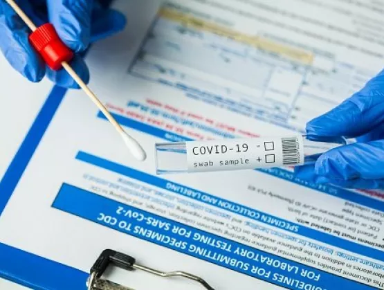
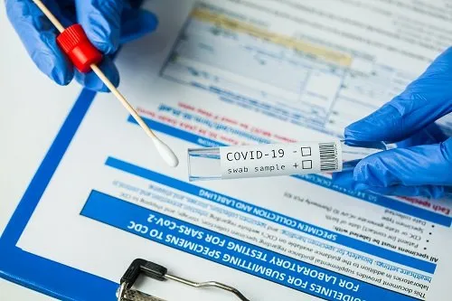
While the world awaits a working vaccine to protect us from COVID-19, we need to employ all available tools to help curb the spread of this novel virus. On the one hand, it’s remarkable that we’re relying on the same low-tech tools that our forebears used to moderate the pandemic of 1918 — social isolation, mask-wearing and hand-washing. On the other, we have access to numerous technologies that hadn’t even been invented a century ago. Among the most important is molecular diagnostics for advanced testing.While we continue to face a scarcity of test kits in the U.S., the majority of commercially available genetic tests for COVID-19 are reliable, so accuracy is rarely the problem. We’re hampered instead by the timeliness of getting the results and by the level of detail the tests provide.To save more lives and reduce the burden on our healthcare system, we need point-of-care genetic tests that deliver accurate results rapidly, telling us right away who’s positive and who’s negative. We also need pertinent test data shared as quickly as possible via secure networks to improve our ability to track surges in infections. These are two of the challenges that emerging biotech companies are pivoting to embrace. RT-PCR: The Gold Standard in Accuracy, Not SpeedWhen I read about some of the high-quality COVID-19 tests on the market – such as Abbott’s, which detects positive results in as little as five minutes — I am awed by how far we’ve come since the last global pandemic. The core enabling technology in test platforms such as Abbott’s uses the molecular genetics technique real-time reverse polymerase chain reaction (RT-PCR). The vast majority of rapid tests administered today in hospitals and other clinical settings use RT-PCR.While accuracy is high for RT-PCR tests, getting tests results to patients is slow because test samples are sent to the lab for analysis. That lab could be located in a hospital, in a doctor’s office, or in an urgent care facility run by a large company such as Quest Diagnostics. Regardless of location, each lab must have an RT-PCR machine to read the test results. Plus each RT-PCR machine costs thousands of dollars, and requires a technician to read the results, , factors that have limited the proliferation of these machines.New COVID-19 cases are still surging in parts of the U.S., India and Brazil, and in some areas, we’re seeing instances of inundated labs, with test results coming back in one to two weeks. That’s not fast enough for a virus this contagious. We need to get accurate tests results to healthcare providers, public officials, and patients as close to real-time as possible. To meet this goal, we need to apply molecular-diagnostic techniques to new types of biosensors that deliver test results at the point of care in minutes through platforms that send that data in near real-time to the cloud. This essential information will allow public health institutions, states, cities and other key stakeholders to identify and mitigate emerging hot spots of disease.Over the past seven months, we’ve had the privilege of working with a handful of biotech companies that have pivoted to develop rapid point-of-care molecular diagnostics that target COVID-19. One of these, HEMEMICS, is developing a handheld molecular diagnostic test platform that could be administered by healthcare workers in triage settings such as ambulances, emergency rooms, community clinics and makeshift hospitals. As a true point-of-care test platform, it would deliver results onsite, without requiring the transfer of test samples to a lab. “We’re aiming to redefine point-of-care testing for COVID-19,” said John Lehman Warden, Jr., CEO and co-founder, HEMEMICS. “Unlike the most common type of on-site test — the lateral flow monitor — our test isn’t waiting for osmotic reactions to occur. We place the sample from a quick nasal swab or a drop of blood right on-chip, and binding takes place within a standing drop of fluid. That makes our platform fast, delivering results in about 60 seconds. Plus it simplifies sharing test results with other communities of interest, such as public health departments and municipalities, because it’s Bluetooth-enabled and supports cloud-based management networks.”As its foundry partner, we’re collaborating with HEMEMICS as it continues to refine its biochip’s sensitivity for both antibody and antigen testing of SARS-CoV-2. Once HEMEMICS is satisfied, it will move forward with the U.S. Food and Drug Administration’s (FDA’s) emergency use authorization (EUA), which it hopes will bring the HEMEMICS platform into the hands of the millions of people who stand to benefit.As we head into the fall and winter months, we’ll need both rapid, connected point-of-care biosensor test platforms such as HEMEMICS’ and high-accuracy RT-PCR tests to fight COVID-19 effectively. And at their root, we’ll have MEMS and biosensors to thank. For more information on Rogue Valley Microdevices’ biosensor solutions, please contact the company at [email protected] or visit its website. As founder and CEO of Rogue Valley Microdevices, Jessica Gomez has created a world-class precision MEMS foundry in the heart of Southern Oregon. Integral to her role as CEO, Gomez practices a business philosophy of offering best-in-class process technology and R D expertise to customers to help them achieve the highest quality and reliability in their products. Gomez plays an active leadership role within and beyond the technology industry. She is a board member of the prestigious SEMI Board of Industry Leaders, she was the first executive selected for Spotlight on SEMI Women, and she is chairman of the Oregon Institute of Technology Board of Trustees.Rogue Valley Microdevices is a longtime member of MEMS Sensors Industry Group (MSIG), a SEMI technology community that enables the MEMS and sensor industry to address common challenges, innovate and accelerate business results.
Read More
MEMS and image sensors are shining stars in the chip industry as technology companies worldwide accelerate innovation in the fight against COVID-19. The tiny devices are behind advances in areas of electronics ranging from thermal imaging and faster point-of-care testing to microfluidics-based polymerase chain reaction (PCR) tools and techniques to detect SARS-CoV-2.SEMI recently spoke with Yole Développement analysts Dimitrios Damianos and Chenmeijing Liang about MEMS and imaging sensors market trends and how microelectronics-enhanced technologies are supporting the worldwide push to contain the spread of COVID-19.For additional insights on the technologies, join the SEMI MEMS Imaging Sensors Summit, held for the first time at SEMICON Europa, 12-13 November 2020 in Munich, Germany. Registration is open.SEMI: Despite the global pandemic, the MEMS and sensors market is still growing and is one of the healthiest industries, not only in Europe, but globally. What is driving this growth?Damianos: MEMS have been continuously evolving from the first sensors that were measuring pressure and acceleration to rotation sensing and visible light management followed by light sensing beyond visible and the expansion to ultrasound and multi-spectral. Now we are heading towards an era where we want to sense every aspect of our environment, with more processing and eventually analytics bringing more quality to the data.COVID-19 has impacted various global markets in very different ways. While automotive, mobility and civil aviation have suffered, the impact on telecommunications and medical has been positive. The effects on the consumer, mobile and industrial markets have been moderate. Moreover, COVID-19 is changing the perception of the current global supply chain in manufacturing, potentially leading to more localized value chains and further regionalization in order to minimize similar risks posed by the pandemic and the first lockdown.SEMI: Who are the main MEMS players based on your research? Damianos: For MEMS players, the picture in 2019 was not the same as 10 years ago, when Texas Instruments (TI) and Hewlett-Packard (HP) were leading the scene, with Bosch and ST Microelectronics following, all at comparable revenue levels. Now, Broadcom and Bosch lead with almost $1.4 billion in revenue each, and the rest of the MEMS key stakeholders compete in the $400 million to $600 million league. Microphone players profited from the voice interface adoption trend, while players active in MEMS for mobility and smartphones suffered slightly due to weak end-system demand.SEMI: What scenarios can we expect for each market with regard to the impact of COVID-19 on MEMS for 2020? Damianos: For 2020, at Yole Développement we expect the consumer market to contract slightly by 2.6%, with the automotive market to dip by 27.5%, and defense and aerospace by 20.5%. For the defense market, no major effect is expected, as all major programs still run for the year. The market may experience some slight delays in deliveries due to supply chain and logistics problems. However, sensors integrated in commercial/civil aerospace applications will suffer due to the general paralysis of the air travel industry. On the positive side, telecommunications could increase by 4.7%, medical applications by 10.6%, and industrial by 11.5%.Due to the global pandemic, some types of MEMS have spiked in demand this year. For example, demand for thermopiles and microbolometers used in temperature guns and thermal cameras has increased because of the need for contactless monitoring of people’s temperatures. Moreover, microfluidics for DNA sequencing and real-time polymerase chain reaction (PCR) diagnostic tests for detecting COVID-19 are gaining market relevance, with the latter serving as a premier method of detecting a bacteria or virus on the molecular level with high degrees of accuracy. Furthermore, pressure and flowmeters in ventilators will grow because of huge demand by hospital intensive care units (ICUs).SEMI: What growth trends do you predict for the long haul?Damianos: In the longer term, we expect global MEMS volumes to almost double, from 24.4 billion units in 2019 to 50.8 billion units in 2025, with a 13% CAGR during the same period. The global MEMS market could reach $17.7 billion in revenue by 2025.We see a trend to more wearable devices integrating a lot of sensors but also a move to a more consumer-oriented healthcare. Moreover, everything related to voice interfaces and voice/virtual-personal assistants (VPAs) will continue to see strong growth, increasing demand for MEMS mics with better quality and high-fidelity voice capture. MEMS devices are shifting to higher accuracy, ultra-low power, embedded intelligence and possibly some bio-compatibility for medical applications.MEMS players will try to escape the commoditization cycle and deliver more value by increasing the value of the data, either grouping many sensors to create sensor hubs or by adding processing, algorithms and software. Industry players are employing strategies such as adding extra processing close to the sensor (e.g. Knowles) or ameliorating the use cases of their applications of their clients (e.g. Bosch or ST). AI on the edge seems very alluring for extra value acquisition, with many startups already working on it. Some examples include always-on-sensing (Aspinity in collaboration with Infineon, Syntiant), echolocation (IMERAI) and predictive maintenance using inertial sensors (Cartesiam). This will be the next pit stop for MEMS technology for sure. SEMI: The CMOS Image Sensor (CIS) is a cornerstone technology in the development of devices powered by machine sensing and artificial intelligence (AI) for applications such as advanced driver assistance system (ADAS). CIS powers many of the ongoing revolutions in new technical products and use cases. What is the status of the image sensors industry? Liang: Last year was exceptional with a combination of high demand and high prices due to capacity limitations. Q4 2019 went way above the forecast, and, in the end, the CIS industry reached $19.3 billion for the full year. This year, we think it will return to normal, and, despite the pandemic impact, we expect significant growth in the range of 7% to 12%. Last year’s 25% year-over-year (YOY) growth was the highest we’ve seen over the past decade. Mobile still dominates the marketplace for CIS with 69% market share. Two markets, computing (8%) and consumer (5%), are adjacent to the mobile market but progressively losing ground due to the smartphone disruption.Security, at 6% market share, will probably be the second largest CIS market in the future. Although this is an area of excellence for the emerging Chinese players, unfortunately, they could be hit by the current trade war. The automotive market did very well from 2018 to 2019 because of the numerous applications recently developed for ADAS, viewing, and in-cabin applications. Lastly, the industrial camera applications benefited from large investments in automation, especially in the semiconductor and automotive industries, but here again many uncertainties remain as these markets will reshuffle in the post COVID-19 world. SEMI: Which CIS markets are most susceptible to seasonality and the impact of COVID-19?Liang: According to our quarterly CIS monitor, automotive and security were both negatively impacted by the pandemic beyond what we expected in terms of seasonality. For computing, the situation improved just prior the lockdown. Q1 got a positive impact with high sales results for laptops and tablets, but no significant impact was seen for security equipment. For automotive, the demand for cameras was very high in Q1, which is seasonally normal, despite the decrease of car shipments that followed later. The automotive CIS market in 2020 should remain relatively flat compared to 2019 due to the higher attachment rates of cameras despite the lower number of cars produced. Consumer and industrial segments dropped in Q1, which is typical early in the year.The next five years might be a bit slow, and although we forecast growth for the next year, in the future the market share will be lower in mobile. In fact, mobile CIS growth will fall below the CIS growth average, but we will see an increase of market share for the security, automotive and industrial segments. The CIS market could reach $28 billion in 2025.At first, COVID-19 had a limited impact on the production side, as factories in China are usually closed for the New Year holiday, when the pandemic started. While supply is currently recovering, we still consider the limited impact on demand. Smartphone production for 2020 will be down 6%, but camera shipments for mobile should increase about 10% this year. Another positive trend for the mobile market is optical fingerprint implementation. Currently, high-end Android phones use this kind of technology. For 2023, we estimate optical fingerprint technology revenue to be over $1 billion.The roadmap for the automotive market is driven by camera proliferation. We’ll see 10 cameras per car and more for some high-end vehicles. Increasing demand for safety and convenience will mean more cameras per car in the future. With a strong attachment rate, the market average in automotive is around 2.0 cameras per car nowadays, and we expect the market average to reach 3.5 cameras per car in 2025. In security, Charge Coupled Device (CCD)-based cameras are nearly out of the market, as CMOS-based IP cameras are most important now.SEMI: What are current key technology trends?Liang: 3D semiconductor technology is the hot topic. CIS wafer staking technology is indeed at the center of the CIS technology race. Future applications could be AI analytics or recently developed applications on new types of CIS. So far, we have seen the introduction of variants of the CIS pixel. Global shutter (GS) and indirect Time of Flight (iToF) were recently introduced, and now direct time-of-flight (dTOF) pixels are being used in high volume. 3D semiconductor technology is a bonanza for the industry, as it allows to pack more value in a single chip. While the surface of silicon is still increasing, additional silicon is added through stacking.With COVID-19 still a problem, the endpoint for smartphones in 2020 remains uncertain. The short-term impact for CIS will be slower growth with respect to the 25% YoY of last year. The downturn in car production will be mitigated by an increased attachment rate for automotive cameras. The security market will also help maintain CIS growth.For more insights, see the following reports: Status of the MEMS Industry 2020 3D Imaging and Sensing 2020 CIS Market Monitor Q2 2020 Dimitrios Damianos is a technology and market analysts at Yole Développement covering MEMS, Sensors, Photonics and Imaging. Chenmeijing Liang is a technology and market analysts at Yole Développement covering Imaging. Serena Brischetto is senior manager of Marketing and Communications at SEMI Europe.
Read More
At UES, Inc., our 300 employees faced a myriad of productivity, logistics, and communication challenges as we responded to COVID-19 yet we continued our work uninterrupted to deliver scientific research and technical expertise to the Department of Defense (DoD). We focus on several disciplines including materials science, aerospace power and propulsion, bio and nanoscale technologies, surface engineering, photonic and electronic technologies, additive manufacturing, and product development.UES is also an active member of SEMI Nano-Bio Material Consortium (NBMC), a public-private partnership with Air Force Research Laboratory (AFRL), and has been a part of the organization since its inception in 2013. Dr. Stephaney Shanks, Director of our newest division, Integrative Health and Performance Sciences (IHPS), is currently acting as the NBMC Governing Council Chairperson. IHPS is setting the standard for high-level research in the Air Force Research Laboratory’s 711th (711 Human Performance Wing) and beyond.Its areas of focus include advancing marker discovery in air and biofluids, sensor development, evaluating microbiomes for health and performance, toxicology, industrial hygiene, and high-throughput screening for genetic and chemical exposure. Most of our employees work at the Air Force Research Laboratory (AFRL) at Wright-Patterson Air Force Base, which is offsite of our corporate headquarters and product development labs.Here are some examples of how our COVID-19 response efforts have not only worked, but helped us thrive during this difficult period, enabling us to continue our vital research for the Air Force and our product innovation work in our corporate labs.1. Pursuing Research Projects to Support COVID-19 SolutionsStaffed primarily by scientists and engineers, UES holds a distinct position in supporting the fight against COVID-19. Our entire organization strongly supports finding solutions to the problems brought on by the pandemic to make life safer for everyone.With our AFRL partners and in our UES labs, we pursued new proposals and began projects to combat the pandemic’s problems. We’re developing rapid devices for detection of breath biomarkers that may indicate COVID-19 infection status to provide non-invasive testing capabilities. We are also pursuing point-of-care devices for real-time assessment of COVID-19 outside of the clinical environment, and we are developing models of the protein spikes of SARS-CoV-2 that could be used to further improve detection capabilities.UES also extended active research toward COVID-19 patient transport on cargo aircraft. We have been working with the 711 HPW to develop computational models to evaluate biological agent dispersal in cargo aircraft.UES is conducting research into the biological agent dispersal patterns in cargo aircraft. 2. Enacting an Effective Work-from-Home Policy and FormatBefore the pandemic, most of our employees did not have the option to regularly work remotely. However, by the end of March 2020, UES needed to respond to both DoD and Ohio government orders to stay at home. This presented new challenges. How do we keep laboratory/bench-based staff working? How do we keep all staff mentally engaged while teleworking?As luck would have it, we moved to Office 365 in February. That technology rollout proved to be a significant advantage in our COVID-19 response. Employees maximized their use of Microsoft Teams by sharing files, collaborating, using chat functions, and hosting video meetings. UES also utilized GoToMeeting for larger group meetings and real-time group file sharing/editing.By late March, our management team provided a tracker file in Excel format for all employees to document daily technical progress. This proved to be an excellent method to track projects, monitor staff COVID-19 symptoms or exposure, and record work location as the AFRL and UES labs began to allow small teams to return. This also kept managers in touch with employees on a weekly basis about ongoing work. It not only created extra layers of accountability, but also demonstrated progress and achievements week to week.Microsoft Office 365 has proved its usefulness to UES during the pandemic. 3. Offering Support to Employees and the CommunityThe overall wellness of our employees and the Dayton region is part of our mission at UES. As we resolved logistical issues and reshaped how we collaborated and delivered results, our leadership team began to focus on how to best support employees and our local community. A few activities supported this effort: We provided masks to all employees, along with an informational visual guide for best practices in wearing and caring for a mask. Safety has been a top priority for all employees. We started offering virtual Coffee Talks and Happy Hours. These company-wide online meetings gave employees a chance to reconnect and share concerns. We also shifted our Fitness Classes to an online format. We utilized our social media channels to engage with employees and share resources. We allocated community support to vulnerable populations (food banks and a domestic violence center). UES gave corporate donations, as well as shared non-financial ways to support the community with employees. This pandemic has brought plenty of challenges, but we're impressed by everyone's innovation and resilience. Every UES team member played an active role in adapting, not just to continue their daily work, but to be a part of the solution and support the community.UES used social media to share remote working tips with employees. Dr. Nina Joshi is president and CEO of UES, an award-winning innovative science and technology company based in Dayton, Ohio that provides its government and industry customers with superior research and development expertise, world-class technical support and value-added management services. A unique philosophy emphasizes passion for advancing science, dedication to superior service and commitment to enhancing careers. Contact the company here.
Read More
Japan’s semiconductor industry has weathered the COVID-19 pandemic to post robust growth. Far from a temporary setback, COVID-19 will lead to enduring change in how we work and live. And just as automation has been a bulwark against the devastating business impacts of the virus outbreak, increasing digitization will lead to new efficiencies in our industry.These were some of the key takeaways from three SEMI Japan Members Day webinars in June and July that offered the latest updates on COVID-19 impacts to the semiconductor industry and restart strategies for SEMI members. More than 2,000 SEMI members across Japan’s islands attended the webinars featuring the following five speakers: Hideki Kanewaka, Marketing Director, Consulting Lead, Japan, Accenture Japan Ltd. Takayuki Komori, Manager, Marketing Engineering Dept, SUMCO Corporation Taketoshi Hamaguchi, Director, Manufacturing Industry, Microsoft Corporation Akira Minamikawa, Senior Consulting Director, OMDIA (Informa Intelligence LCC) Yuichi Koshiba, Managing Director Partner, Boston Consulting Group COVID-19 Impact on Japan Semiconductor Industry is ModestThe consensus view of the five speakers from various quarters of the industry – consultant, IT service provider, materials supplier, market analyst – was that the Japan semiconductor industry withstood the heavy blows COVID-19 dealt to other industries thanks to strong demand for chips. Shelter-in-place policies and lockdowns spawned by COVID-19 has accelerated the digital transformation rippling around the world as electronics sales have soared to support everything from remote work and education to healthcare and home entertainment including gaming.The rapid growth of cloud usage for video streaming, gaming and remote work is taxing communications network capacity and placing more bandwidth demands on servers, said Akira Minamikawa of OMDIA. According to a recent report by Nokia, communications network traffic has skyrocketed 300 percent for online meetings and 400 percent for gaming, bringing the networks closer to their capacity limits. Minamikawa sees server shipments increasing at 8 percent CAGR through 2024. For the broader chip market, he expects demand for notebooks, solid state and hard disk drives, and gaming to remain strong in 2020. He also predicts rapid 5G penetration for smartphones will boost semiconductor chip industry growth.Still, not all semiconductor segments are expanding, said Yuichi Koshiba of Boston Consulting Group. Chip shipments for end products in markets such as automotive, industrial equipment and aircrafts are on the decline. Slowing demand for chips that power automotive applications in particular could pare sales for some chip companies and distributors since the segment accounts for a high proportion of their overall revenue.State of the Semiconductor IndustryFrom SUMCO’s vantagepoint as a major silicon wafer supplier, the company’s Takayuki Komori sees a number of changes unfolding in the semiconductor industry: Smartphones are driving growing demand for process technology (smaller nodes) and 300mm wafers. Komori estimates the typical high-end smartphone sports 1,700 square millimeters of silicon. 300mm wafers account for 80 percent of that total while more than 50 percent of the devices use leading edge multi-patterning technologies. Smartphones will need more RF chips to support 5G’s high-speed communications and added frequency ranges. Substrates for RF switches and tuners have been shifting from gallium arsenide (GaAs) and other compound semiconductors to silicon. 5G smartphone penetration will accelerate as the cost of integrating CPUs and modem functions into a single chip sees a swift decline. While the sensitivity and resolution of CMOS image sensors have evolved to incorporate innovative backside illumination and stacking technologies, future advances will focus more on products for machine vision applications capable of sensing invisible light bands. Rising adoption of electric vehicles and robotics applications will drive growing demand for power semiconductors that control their motors such as IGBTs and MOSFETs as the production capacity for the devices expands and shifts to 300mm wafer lines. For memory fabs, Minamikawa said utilization remains high as a result of a spending slowdown by major chip manufacturers and will stay elevated even once additional capacity ramps to support robust demand. Foundry fab utilization also remains high despite the pandemic-driven cancellation of smartphone chip orders in March. Minamikawa also sees the utilization rate of micro rising with the surge in demand for notebooks, PCs and servers in the second half of 2020.Transition to New NormalAs people around the world start to settle into new ways of living and working, there’s a growing acceptance that the transformation will be long-lasting. And no area of people’s lives is changing more than their work. Boosted by government subsidies, many small and midsize companies in Japan have started to implement work-from-home policies, an area where major electronics and IT businesses had already instituted reforms, said Hideki Kanewaka of Accenture. A few examples: Nippon Telegraph and Telephone Corporation (NTT) announced that half of its employees will continue to work from home in the future. A five-year plan Toshiba launched in 2019 to allow all employees to work from home will likely accelerate. Hitachi plans to allow all employees to work from home starting in April 2021. dwango, a major internet-based entertainment company in Japan, announced it will allow in principle any employees to work remotely. In the critical area of remote sales, Kanewaka pointed to the importance of going beyond online business meetings, paperless transactions and virtual events to devise new ways to attract customers and close deals. Creating online communities and providing rich digital content are also important measures to consider, he said.Manufacturing's Digital TransformationTravel restrictions by most countries to curb the COVID-19 outbreak have also raised barriers to chip companies sending engineers overseas sites to service state-of-art equipment and provide other technical support. Microsoft’s remote assist system deployed by ASML is one tool semiconductor makers can use to overcome this challenge, said Taketoshi Hamaguchi of Microsoft.The system connects a remote equipment service expert with an onsite worker through the internet, allowing the technical expert to provide support through a goggle display with a camera worn by the worker. Guided by the expert, the worker can perform complex services. A Natural User Interface (NUI) helps give the factory worker a clear understanding of the often highly technical instructions.Using artificial intelligence (AI) to increase automation will also help reduce the reliance of semiconductor factories on onsite workers. For example, AI deep learning can be deployed to calibrate equipment autonomously and reduce downtime after scheduled maintenances, Hamaguchi said.Corporate Restart Strategies Beyond factory considerations tied to COVID-19, semiconductor companies will need to adapt their business strategies to new ways of operating. For example, global supply chains will shift to domestic sources and increase redundancy to ensure a steady supply, a change leading to higher overall costs, Koshiba said. Trade routes among regions will also be redrawn as the trade rift between the United States and China and other geopolitical tensions intensify. The total value of those routes is expected to recover by 2023.Koshiba advised companies to evaluate the supply chain trade-offs between stability and cost and factor in potential risks to improve their short-term resilience and drive mid- to long-term supply chain restructuring.After past recessions, 14 percent of companies restored sales growth, Koshiba said. He recommended investing aggressively in growth and seizing M A opportunities during the downturn. Chip companies must also adapt to supply chain changes faster than competitors.Become a SEMI MemberWebinars like the recent SEMI Japan Members Day series have become increasingly important in the mix of programs and services SEMI offers members to help them connect, collaborate and innovate in the microelectronics community. To become a SEMI member, please visit the SEMI website or contact your nearest SEMI office.Jim Hamajima is president of SEMI Japan.
Read More
Why do we need environmental air pollution sensors?Today we need environmental air pollution sensors more than ever to ensure that we have clean and safe outdoor and indoor air. Although federal rules have improved air pollution over the past several decades, more than 110 million Americans still live in counties where air quality is below national standards. An estimated 100,000 Americans die prematurely each year of illnesses caused or exacerbated by polluted air.“Cars and trucks are much cleaner than they were, power plants are cleaner, industrial operations are cleaner,” said Paul Billings, Senior Vice President Advocacy for the American Lung Association. But cleaner air is not clean air.”While scientists have long known that air pollution may exacerbate asthma and other respiratory illnesses, new data suggests polluted air leads to higher COVID-19 higher death rates and brain inflammation that can contribute to dementia and autism.To understand the importance of air quality and how we can apply existing sensors and develop new ones, we look both outdoors and indoors (see Figure 1). Outdoor air quality relates to gaseous and particulate pollutants, defined by the Air Quality Index (AQI). The AQI became a standard based on regional thresholds for a set of key outdoor pollutants: four gaseous pollutants (sulfur dioxide, nitrogen dioxide, carbon monoxide, ozone) and particulates (PMs) of different sizes such as 10 μm (PM10) and 2.5 μm (PM2.5). At present, the AQI is measured using traditional analytical instruments. Despite their high acquisition and maintenance costs, these instruments are the only solution to accurately measure these pollutants in the presence of variable environmental background.Figure 1. Examples of outdoor and indoor air quality markers Indoor air quality (IAQ) is also of growing concern. Formaldehyde, benzene, carbon monoxide, and carbon dioxide are some of the key pollutants with restricted concentration levels in residential, office and industrial buildings. Sources of these and other gaseous pollutants include building materials and equipment, workplace cleansers, and building occupants. Regulatory agencies and building occupants use different methodologies to estimate IAQ using gaseous and particulate pollutant analyzers. These estimates also consider air humidity and temperature that affect indoor air quality. Where are we today with environmental sensors?The top three requirements for modern gas sensors include: the sensor reliability to provide accurate readings in diverse environmental conditions over desired period of use low power, to extend battery life or to eliminate its need, and low cost, to facilitate their ubiquitous deployments. Advances in electronics, microfabrication, and packaging have delivered recent important developments in reducing the power consumption and miniature packaged solutions. Recent R D efforts are also increasing the number of successful gas sensor field deployments for outdoor and indoor air quality monitoring. Figure 2 illustrates three examples of recent developments in gas sensors that meet requirements of diverse customers.Electrochemical sensors from SPEC Sensors were collocated with EPA instruments for monitoring of NO2 and O3 in Chicago’s Array of Things Project. Figure 2A shows that these new cost-effective sensors track well the EPA instruments. Advancements in circuit quality, sampling, enclosure design, and initial calibration/compensation were all essential in achieving these results. While this example clearly demonstrates the usability of these sensors in this particular application, the expectations that low-cost, off-the-shelf sensors will match the performance of EPA reference systems that cost 50x-100x more must be adjusted. A micropackaged sensor suite from Bosch Sensortec includes sensors for total volatile organic compounds (TVOCs), temperature, humidity, and pressure. TVOC measurements are needed according to the guidelines by the German Federal Environmental Agency. To report TVOC, the sensor algorithm tracks the TVOC-related resistance of the metal oxide sensor, corrects sensor resistance for ambient temperature and humidity, and outputs the TVOCs Index of Air Quality between 0 (clean air) and 500 (heavily polluted air) as shown in Figure 2B. A recent GE-developed dielectric excitation scheme of metal oxide sensing materials provided a highly desired and long-awaited calibration stability of sensors for monitoring of fugitive methane gas emissions in all-weather conditions. These sensors were used in several field validation campaigns in Oklahoma, North Dakota, Arkansas, and British Columbia and had stable performance after more than 400 days, as compared to an initial calibration (see Figure 2C). Such stable sensor performance has become possible by switching from the conventional resistive mode of operation of metal oxide sensing elements to the dielectric excitation scheme. Figure 2. Examples of applications of contemporary gas sensors based on different detection principles.(A) Outdoor performance of NO2 and O3 electrochemical sensors versus EPA-validated instruments.(B) Calibration results of a BME680 metal oxide gas chemiresistor upon exposures to TVOCs (blue stair-profile) and its ± 15% confidence interval band as the Index of Air Quality.(C) Calibration stability of a sensor with an innovative dielectric excitation scheme implemented for monitoring of fugitive methane gas emissions after multiple uses in diverse field validation campaigns. Key challenges and solutions toward realizing new applicationsIn this era of data-on-demand, environmental sensors could enable countless new applications. Imagine you have a gas sensor conveniently integrated into a smartphone or a watch. You are commuting to work, and your sensor alerts you that the subway station through which you are traveling has very poor air quality. How might this alert affect your behavior? Would you put on a mask, change your commuting route to a twice-longer one, or petition the city? What if you are attending a parade downtown with your asthmatic child, and your device informs you that the air is clean? Would you skip the parade if you knew that your sensor was only 10% accurate? How would you avoid a risk of ending with your asthmatic child in a hospital?Design principles of modern sensors originate in the 20th century for detection of high gas levels from leaks, but they did not anticipate the applications proposed now. By design, existing sensors have only a single output – e.g. resistance, voltage, current, light intensity – that mathematically cannot correct for the sensor instabilities caused by the complex chemical background and variable temperature and humidity conditions. Thus, often these simple sensors perform best when pollution levels are high and when the compound of interest swamps others. As a practical example, there are dozens of gaseous pollutants in ambient air with their toxicity that differ 1,000-10,000 fold. Often, the insufficient reliability and accuracy of existing sensors in the field conditions is a significant bottleneck toward the broad adoption of gas sensors. According to the United States Environmental Protection Agency (EPA), the correlation between readings of low-cost sensors versus reference monitors varies widely from 1% to 80%. The EPA also states that no low-cost sensors meet Regulatory Monitoring requirements, and the World Meteorological Organization emphasizes that “low-cost sensors are not currently a direct substitute for reference instruments, especially for mandatory purposes.” However, we now have the increasing number of examples of reliable operation in complex environments (Figure 2) in addition to important advances in reduced power and size of contemporary sensors. Still, the key challenges to realize new applications are often the lack of required accuracy and reliability of available sensors for new contemplated applications.Is it possible to offer low-cost sensors for at least some applications and some gases with the degree of accuracy approaching more expensive specialized instruments? We, the SEMI-MSIG Device Working Group, are saying: Yes. To deliver on this bold statement, our SEMI community brings new technological solutions to the 100-year old general design of gas sensors.Our next blog What is in the Air will provide details on our activities of SEMI-MSIG Device Working Group to establish standards and new measurement schemes to reduce effects from uncontrolled ambient conditions and to improve stability, limit of detection, and dynamic range of environmental sensors. Also learn how new MSIG members can impact this important working group. The MEMS Sensors Industry Group (MSIG) is a SEMI technology community that enables the MEMS and sensor industry to address common challenges, innovate and accelerate business results.Radislav A. Potyrailo is Principal Scientist, Micro Optoelectronics Gas-Chem-Bio Sensors Systems, at GE Research; Ed Stetter is General Manager at SPEC Sensors, LLC; Ryotaro Sakauchi, is Senior Manager of Business Development at Bosch Sensortec; Merry Smith is a Product Manager and Senior Scientist at C2Sense, Inc.; and Sreeni D. Rao is Senior Director of the MEMS Business Group at TDK Corporation.
Read More
I recently spoke with Andrew Goh, Vice President at General Manager at Lam Research Southeast Asia, about the importance of the company's new production facility in Penang and its COVID-19 relief efforts. Ng: Before we delve into details, please provide a quick introduction to Lam Research Southeast Asia for our readers who aren't as familiar with your work. Goh: As you know, Lam Research is a leading supplier of wafer fabrication equipment and services to the global semiconductor industry. Since we were established in 1980, Lam has played a key role in contributing to the extraordinary pace of innovation in the semiconductor industry. We have always developed innovative solutions that help our customers build smaller, faster, more powerful, and more power-efficient electronic devices – the kind that are driving the proliferation of technology in our everyday lives.Further to this, we established Lam Research Southeast Asia in 1992 to better serve our customers in this region. We have about 260 employees in both Malaysia and Singapore, with more than two-thirds of them in engineering or technical roles.Ng: Early this year, Lam Research announced a new advanced technology production facility in Malaysia. Please tell us about it.Goh: Yes, Lam Research and the Malaysian Investment Development Authority jointly announced in February 2020 that Lam selected Batu Kawan Industrial Park in Penang, Malaysia as the location for a new advanced technology production facility.Our new state-of-the-art manufacturing site in Penang’s Batu Kawan will open in May 2021 and be the largest in our network. The current plan envisions a 700,000 square-foot facility with expansions already anticipated to serve current and future customers. Construction started in May 2020, and we aim to have our first shipment by 2021. We are currently at our temporary site in Bayan Lepas.Ng: As Lam’s manufacturing site, what role does it play in the larger organisation?Goh: The semiconductor industry is expanding and so are we. To help our customers move the world forward, we need a dynamic, energized team with initiative and focus to help establish our footprint in Malaysia. This has led to the expansion of our existing global production footprint with locations in the United States, South Korea, and Austria. As the industry moves forward, we at Lam Manufacturing Malaysia will work on the entire portfolio of our leading-edge products, collaborating closely with customers to create some of the world’s most sophisticated processes and fabrication equipment. We chose Penang for its talented workforce with experience in aerospace, health sciences manufacturing and other high-tech fields. We are currently hiring now for our site in Penang. Anyone interested in exploring job opportunities at the site can send learn more and apply at www.MakeAtLamPenang.com. Artist's rendering of new Lam Research production facility at the Batu Kawan Industrial Park in Penang. Ng: With the world now thrown into an unprecedented situation, do you expect any delay in the construction schedule?Goh: Despite the COVID-19 pandemic, construction began in May 2020. We still expect to make our first shipment from the Batu Kawan factory around mid 2021, in line with our initial estimates. Close cooperation with and timely support from MIDA and Invest Penang have allowed us to stay on track.Ng: How has Lam done supported COVID-19 relief or recovery efforts during this pandemic?Goh: Just as with any other business, this pandemic indeed is a trying time for all of us around the world. We announced on April 8 that we are donating $25 million to global COVID-19 relief and recovery efforts, which includes relief funds to employees, employee benefit resources, and additional support for the areas in which we operate. This support includes supplies for hospitals, both short-term and long-term community assistance, and our 2-for-1 gift matching for eligible COVID-19 relief programmes.In addition to the fund, we have also donated our surplus inventory of masks for immediate relief to local hospitals. At the same time, our innovative engineers and others with 3D printers at home have begun developing prototypes and printing protective face shields.Consistent with current guidance from the U.S. as well as the region’s respective Centers for Disease Control (CDC) and World Health Organization (WHO), we have activated our business continuity plan (BCP) to safeguard the health and well-being of our employees and their families, as well as to mitigate business disruptions to our customers. Measures we've implemented include strict social distancing, quarantine measures and travel restrictions.Bee Bee Ng is president of SEMI Southeast Asia.
Read More
A lot has happened in fifty years, particularly when it comes to the microelectronics industry. Founded in 1970 by a group of semiconductor industry pioneers who believed that co-opetition — instead of traditional competition—would produce a more vibrant emerging industry, SEMI was born as an industry association.It's fitting during this week’s 50th annual SEMICON West (July 20-23, 2020) — a virtual event for the first time — that SEMI Chief of Staff Bettina Weiss offers her perspectives on the evolution of SEMI from one of the best seats in the house: the 24 years that she has spent helping the association change and grow.Vetrano: You’ve enjoyed a long rich history with SEMI, and now serve as the association’s first chief of staff. What roles have you played at SEMI up to this point?Weiss: I cut my teeth at SEMI by joining SEMI Standards, first serving as standards coordinator at SEMI Europe from ’96-’97. Over the next 11 years, I held a variety of positions at SEMI Standards, culminating with director of international standards from 2003-2008. Given that experience, I have to admit that SEMI Standards are still near and dear to my heart.I moved on to several leadership positions in our former global photovoltaics/solar business through 2014, and toward the end of that stint, I assumed additional responsibilities, becoming vice president of business development. That’s where I dove headfirst into expanding SEMI into emerging regions, including Vietnam, India and Latin America. SEMI goes where members see (or want to better understand) new opportunities, especially in places that had ambitious plans for fabs for microelectronics, including semiconductors and MEMS.In 2018, I became SEMI chief of staff, reporting directly to our president and CEO Ajit Manocha.Vetrano: Now I hardly know where to start! Since I have to decide, what does it mean to be SEMI chief of staff?Weiss: As the first chief of staff, I’ve been able to shape the position, combining the support of critical efforts driven by Ajit with additional project management responsibilities like our Smart Mobility initiative.Working with experienced leaders in our industry, such as the Board of Industry Leaders (BIL), is one of the more rewarding parts of my role at SEMI. The BIL is a group of global executives tasked with advising SEMI on strategic planning, especially when it comes to future-looking initiatives like Smart Mobility, Smart MedTech, Smart Manufacturing, and Smart Data/AI.A lot of the other things I do are meant to support the whole SEMI organization, in partnership with other senior leaders such as Michael Ciesinski, vice president of technology communities, as we create business plans and examine new revenue models that will keep SEMI sustainable and viable for the future. This includes issues as varied as workforce development and diversity and inclusion, and the new digital platforms we use to engage with our members.Vetrano: How does SEMI Smart Mobility initiative exemplify the model of engaging end customers in vertical markets that are important to members?Weiss: When you look at the rapidly increasing number of chips and sensors in and around vehicles, Smart Mobility at its core brings together both the semiconductor/sensor and automotive/mobility supply chains for a more transparent dialogue about needs and wants along the entire supply chain. We are thrilled to count automotive OEMs Volkswagen and Audi as SEMI members. We also work with Tier 1 suppliers such as Continental and many others to promote the open exchange of ideas and foster collaboration among all stakeholders.Smart Mobility is a good example of how SEMI connects two worlds that are now interdependent for the mutual benefit of all players. Automotive companies and component suppliers want to better understand new technology capabilities that enable tomorrow’s infotainment, safety, security and communication protocols. And semiconductor, sensor and component companies see huge upside in supplying the equipment, materials, devices and subsystems that enable the future of mobility. Smart Mobility is a win-win, and the founding concept of our Global Automotive Advisory Council (GAAC).Vetrano: As we look to COVID-19, the single most important event to influence the microelectronics industry — and every other industry — why is SEMI membership more important now than ever?Weiss: Our industry is facing a triple whammy of challenges: a global pandemic, ongoing global trade tensions that impact interdependent supply chains, and a global economic crisis. All these challenges will require our members’ ingenuity, innovation and collective action to overcome them. But inherent in those challenges are tremendous opportunities, and I have no doubt that our members and the entire global electronics ecosystems will find ways to help everyone prosper and advance.COVID-19 has had a huge impact on our members. From the onset of the pandemic, we’ve provided our members with resources including best business practices, insights and data from industry experts to help them respond to a virus that has already changed so many things we took for granted before March. Additionally, SEMI has also advocated with governments around the world on behalf of the industry for essential business status and essential travel to sustain operations. Visit SEMI COVID-19 Resource page for information on industry best practices and much more.Vetrano: Before we look forward, what has changed dramatically in microelectronics since you started at SEMI?Weiss: Through my work with SEMI, I’ve witnessed dynamic, dramatic and sustained change in the microelectronics supply chain. Into the late 1990s, SEMI represented primarily semiconductor equipment and materials suppliers, and we worked with chipmakers – our members’ customers. That’s where a lot of important Standards work happened, for example, and the supplier-device maker relationship was pretty much our world. Over the years, we saw significant change in how companies partner and do business with one another. The digital transformation we’ve been witnessing for the past few years was the impetus for expanding our reach to bring companies in the extended electronics manufacturing and design supply chain together, from sand to system, so to speak. That was also when we invited associations representing flexible hybrid and printed electronics (FlexTech), MEMS and sensors (MSIG), and electronic system design (ESD Alliance) companies to join SEMI and our other technology communities for maximum cross-pollination. That’s because everything needs microelectronic devices and systems. Vetrano: Looking ahead now, what is can the microelectronics industry do to benefit humanity?Weiss: Semiconductors and sensors are often the unsung heroes of progress. Microelectronics can help bring prosperity to the billions of people now struggling on our planet. It can improve access to education for people through e-learning, it can advance agricultural production and streamline the food supply chain to help feed the world’s hungry, it can monitor the quality of the water we drink and the air we breathe, and it can get you in front of a doctor even in the most remote village in India.The beauty of microelectronics is that we are not gated by innovation. As the brilliant visionary Arthur C. Clarke once said, “The only way of discovering the limits of the possible is to venture a little way past them into the impossible.”As an industry association that helps technologists to venture beyond “the limits of the possible,” I invite like-minded technology adventurers to engage with SEMI, starting with registration to this week’s SEMICON West – our first virtual show.As chief of staff, Bettina Weiss reports to SEMI President and CEO Ajit Manocha and manages a broad portfolio of responsibilities. Major focus areas include advancing specific global strategic initiatives such as thought leadership (Think Tanks) and SEMI Smart Transportation vertical application platform, improving organizational efficiency, alignment and financial sustainability, acting as senior liaison to SEMI Board of Industry Leaders, leading strategic partnerships and M A activity, and supporting Manocha in creating a highly effective, agile global association.Maria Vetrano is a PR consultant at SEMI.
Read More
The COVID-19 pandemic has inflicted major impacts on manufacturing operations worldwide including in the semiconductor industry. The virus has left millions of people confined to their homes, resulting in a massive shift to virtual work and online engagement. In Singapore, where AEM is headquartered, our management team took proactive measures to protect our workers by implementing best practices ahead of the Singapore Circuit Breakers.AEM is globally deemed an essential service, requiring us to maintain operations and minimize impact to our customers. Business continuity plans that include work-from-home and safe-distancing guidelines are in place. As of the time of this writing, we are very fortunate that all of our employees are safe and that we’ve seen only minimal impacts to our customer commitments. AEM has confined this impact by spreading operational risks across our facilities in Asia, Europe, the U.S. and divisions in Singapore, Malaysia, China, North America, Central America, Finland, France and Vietnam. All told, these facilities employ more than 550 people (Figure 1).Figure 1 – AEM Global Presence As a global leader, AEM offers application-specific intelligent system-level test and handling solutions for semiconductor and electronics companies that serve the advanced computing, 5G communications and artificial intelligence (AI) markets.Leveraging our decade of experience, the latest AMPS solutions provide asynchronous, modular, massively parallel and smart system-level testing to meet the new test challenges of complex ICs. The modularity and scalability of these systems enables customers to scale their existing engineering device validation solutions into high-volume, massively parallel production solutions that increase faults coverage, reduces time to market, and decreases cost of test and ownership (Figure 2).Figure 2 – AMPS System-Level Test Solution In meeting 5G infrastructure test needs, AEM developed a field-deployable fiber optics tester. Called WideOptix SR4, the system was initially developed in collaboration with a world leader to support the 5G fiber infrastructure deployment in China and has now been adopted for some Ethernet standards testing. With our WideOptix SR4 development, we cultivated Silicon Photonics (SiPh) testing expertise that complements our AMPS system-level test capability. As part of our business continuation and risk diversifications plan, we had also set up factories in Penang (5,200m2) and Suzhou (3,600m2). Penang’s rising influence in the Southeast Asia semiconductor industry has prompted AMM (AEM Malaysia) to expand its scope to include value-added services with a Center of SSD Excellence and Center of Photonic Excellence.ASZ (AEM Suzhou) will continue to focus on the domestic market in China for further expansion and penetration with products ranging from cost-sensitive testers to state-of-the-art test measurement instruments. In Europe, AEM is focused on wafer-level test and cost-effective ATE test solutions. Finland-based AFORE specializes in MEMS and application-specific wafer testing with the ability to add physical stimulus. The company's state-of-the-art instruments enable the testing of devices such as diced IMU’s (Inertia and Motion Units) in continuous rotation on a wafer mounting ring. Our process increased test throughput by 3X compared to the traditional pick-and-place methods (Figure 3).Figure 3 – Wafer-Level Test Throughput Advantage A specialist in application-specific wafer handling, AFORE developed its latest design to support quantum computing in collaboration with its partner BLUE FORS. The company’s probing equipment features a handling solution with temperature tolerances to 2K (-270’C) to support cryogenic testing (Figure 4).Figure 4 – Cryogenic Quantum Computing Probing Solution AFORE also gained critical insights into creating total darkness, enabling us to further explore opportunities for dark matter testing. AFORE is currently in talks with a member of the LUX Photonics Consortium funded by the National Research Foundation (Singapore) to provide a dark body testing environment and handling for its IR detectors.In Europe, our acquisition of Mu-TEST in France helps diversify our product and service offerings while spreading our business continuity risks. Mu-TEST enjoys collective test-development experience of more than 320 man-years thanks to various ATE suppliers including Schlumberger and Credence. To help combat rising costs of traditional ATE, Mu-TEST developed cost-effective solutions using FPGA-based instruments supported by a full suite of test development, debug and production test software with links to EDA and standard interfaces. This provides Mu-TEST an agile platform that can be easily re-configured for different customer needs.This Mu-Test acquisition expands AEM’s system-level testing capability to include Functional Test, allowing BIST, SCAN, JTAG to test structural failures and perform other application-level test that interface directly with the DUT using the EVM (Electronics Validation) boards to increase fault coverage within the same test environment. Mu-TEST has also enabled AEM to form the recent partnership with UTAC to develop a cost-effective CIS test solution that addresses UTAC’s test needs and complements its CIS advanced packaging solutions. Our U.S. headquarters based in Chandler, Arizona has expanded its capabilities to provide application engineering.In summary, AEM has been expanding its global footprint while managing risk and has been fortunate to be positioned to manage the recent COVID-19 excursions. While each geographical location specializes in core technologies, all sites have access to one another’s manufacturing facilities in times of need and a pool of IP available to address new opportunities. We believe this risk diversification positions us well to serve the needs and interests of our customers worldwide.Lo Wee Tick is Director, Business Development, and Stuart Pearce is Senior Director, Field Marketing, at AEM Holdings Ltd.
Read More
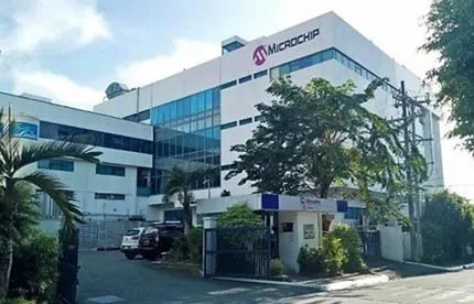
As the COVID-19 quarantine-related restrictions for commerce and transportation are lifted in the Philippines, companies are dusting off desks, cleaning coffee mugs, warming up equipment and gradually bringing back staff to resume full operations. Of primary interest to manufacturing companies like Microchip Technology Philippines are the restrictions on the allowable workforce, the movement of personnel, transportation, and health and safety protocols affecting factory staffing, materials availability, and the ability to ship products. In the Philippines, these restrictions started to scale back in mid-May and are staged to continue in a series of continuing reductions every two weeks through the end of June. As business operations recover, challenges remain in managing the workforce, negotiating the supply chain and understanding the expenses required to operate under the “new norm” while Business Continuity Plans continue to be reviewed and revised.Here are some of the more important business-related elements of the quarantine levels enacted by the Philippines:Enhanced Community Quarantine (ECQ): In effect from March 17 through May 15, 2020, this was the initial lockdown with the strictest requirements, most notably requiring the general population to stay at home, imposing curfews, prohibiting all public gatherings including schools, halting public transportation and banning air travel while allowing cargo flights, skeletal workforces (~15%) for essential businesses (BPOs, IT and exporters, for example) and travel using some private vehicles with varying types of passes required to clear checkpoints.Modified Enhanced Community Quarantine (MECQ): In effect from May 16 through May 31, 2020, this was the first stage to ease control to allow up to 50% of employees to return to work at essential businesses. The easing also allowed gatherings of up to five people while maintaining most other restrictions.General Community Quarantine (GCQ): In effect from June 1 through June 15, 2020, essential businesses are allowed to resume full operations within health and safety protocols in place for physical distancing, disinfection and the wearing of Personal Protection equipment (PPE). Air travel is allowed to resume while public transportation remains restricted until June 21, 2020. Company shuttles are allowed for point-to-point services.Modified General Community Quarantine (MGCQ): Planned for June 16 through June 30, 2020, this is the transition phase to the “new normal,” which will continue easing the restrictions for contact-related businesses such as barbershops, salons, restaurants and the like. Movement and public transportation will remain restricted until June 22, at which point the last obstacle for businesses to fully resume operations will fall.While some larger companies during the most restrictive ECQ were able to house staff on site or nearby in skeletal crews, some smaller companies were unable to do so and may never recover from the loss in revenue or from the loss of employees. The majority of companies in the technoparks shut down under the ECQ and were rendered powerless to return workers to factories. For factories allowed to house employees on site, a huge effort was required to provide emergency transportation, accommodations, food and drinking water, toiletries, Wi-Fi, and even entertainment for the sequestered staff – all while maintaining health and safety protocols for physical distancing and disinfection. For example, Microchip Technology Philippines was able to build temporary sleeping cubicles and showers; to buy tents, foam mattresses, bedding and personal hygiene kits; to provide canteen and laundry services; and to allow Wi-Fi access for employees to stay connected to family and friends.Microchip Technology’s 11 Guiding Values help to define our corporate culture and guide our decision-making. One key Guiding Value on display as we’ve transitioned through the levels of quarantine due to the COVID-19 pandemic has been that Employees Are Our Greatest Strength. Exercising this Guiding Value has supported the expenses necessary to provide the safest, most comfortable living accommodations in the factory conference rooms, hallways, basement, and even in office cubicles.While many larger companies in the Philippines provide company shuttles at pre-established pick-up points, limited public transportation strands many workers at home with no way to reach to their assigned shuttle. To address this challenge, solutions including van brigades that can navigate narrow village streets to pick up workers should be considered though at an additional, unplanned expense. The physical distancing rules effectively halves the number of riders, which in turn requires a doubling of the shuttle buses, most of which are under lease. If shuttle bus leasing companies cannot provide more buses, employees who can work from home should continue to do so or drive to shuttle stops if they have personal vehicles. Leasing these additional shuttle buses was in no company’s budget as we began 2020.Additional measures under the new norm will be expensive – perhaps prohibitively so – for smaller companies that cannot afford to double the number of company transports due to physical spacing rules requiring them to halve workplace capacity, whose workplace environments cannot support physical distancing, and whose treasuries cannot afford to buy rapid test kits for employees and their families. If these smaller companies produce items critical to the supply chain, larger companies will feel the sting – and cease producing specific products during the qualification of an alternate supplier. Until the Bureau of Customs and staffing of third-party logistic providers is back to normal, and until ports are running at full force, materials and exports will continue to be delayed, potentially limiting the number of employees needed to return to work to run production.It has been very expensive for companies to survive through these levels of quarantine while keeping factories and employees in a state of readiness to return to work. Additional expenses will be borne for compliance to the new norm. As many businesses recover under the new norm, they’ll undoubtedly take a closer look at their business continuity planning, if any such plans exist, and if not, they should be created without hesitation.The problem with a typical business continuity plan is it tends to focus on one or a few concurrent major events – say, flooding or a power failure due to a typhoon – but it’s doubtful any plan took into account a global pandemic that affected so many factors simultaneously including workforces, supply chains, transportation, logistics and food supplies. As we return to work, we’ll have to adjust to the new workplace and embed the lessons learned during the COVID-19 pandemic into our business continuity plans. And, hopefully, we’ll never have to exercise those measures again.Greg Fisher is Managing Director at Microchip Technology Philippines.
Read More
Semiconductor companies that begin revising their long-term strategies now may emerge stronger in the next normal.In the months after the coronavirus began to spread, semiconductor companies moved decisively to protect employees, secure supply chains, and address other pressing concerns. Although the situation is still serious and many governments are still imposing physical-distancing requirements, semiconductor leaders are now looking ahead to the time when the pandemic abates and the next normal begins. To prepare for that moment, they are thinking about strategies for reimagining and reforming their business models—two activities that McKinsey described in a framework for responding to the coronavirus.Every aspect of the business model could be subject to change, including the composition of product portfolios, capital expenditures (capex), R D strategy, demand forecasts, supply-chain footprints, production decisions, and options for mergers and acquisitions (M A). But with so much uncertainty ahead, semiconductor companies may have difficulty making strategic decisions. To move forward, they should first establish a solid baseline for their company (see sidebar, “Determining the starting point,” for more information on this topic). With this foundation, semiconductor companies can chart a path to the next normal by focusing on the following questions: What recovery scenarios are most likely, considering evolving demand, economic developments, and other global changes? What is the impact of the COVID-19 crisis on long-term trends and demand? How can we emerge even stronger from the crisis? In past downturns, companies that thought about strategic questions early in the crisis were most likely to recover quickly and become market leaders. Although the COVID-19 pandemic is unprecedented in modern times, the need for long-term planning still holds true.Developing recovery scenariosCOVID-19 has significantly altered the fundamentals of the sector, including customer behavior, business revenues, and numerous aspects of corporate operations. Many companies have unclear future prospects, and some may not survive the crisis. Multiple recovery scenarios are possible, depending on potential government interventions and other variables that are now difficult to predict.Earlier, we published an article about the short- to medium-term outlook for semiconductor demand. Our analysis was partly based on assumptions in two of the nine scenarios that McKinsey developed for the COVID-19 recovery, both of which assume that the spread of the coronavirus is eventually controlled and catastrophic economic damage is avoided. In the first scenario, termed A3, global gross domestic product (GDP) recovers in the fourth quarter of 2020; in the second, termed A1, recovery is delayed until late 2022. Since the original analysis, we have updated the estimates to include 2021 demand.Both recovery scenarios suggest most semiconductor segments will experience negative year-on-year revenue growth in 2020.Both recovery scenarios suggest that most semiconductor segments will experience negative year-on-year revenue growth in 2020. Looking ahead to 2021, however, we expect that the situation will improve as most end markets recover, mostly because the starting point for 2020 will be much lower than it was in previous years. In the more optimistic A3 scenario, only a few segments meet the growth expectations that were forecast before COVID-19 emerged by 2021 (Exhibit 1). In the more pessimistic A1 scenario, the number of segments that recover is even lower (Exhibit 2). Within the individual segments, a few trends stand out: PCs. This segment will see the sharpest drop in demand and the performance gap will become more serious over time. Most people will buy all the home-office electronics that they need for remote work in 2020, lowering demand for next year. Meanwhile, enterprises may continue to delay investments in PCs to control expenditures, even if the recovery is proceeding. Automotive. In the more optimistic recovery scenario, A3, the automotive segment sees year-on-year growth of 28 to 36 percent in 2021. This estimate is based on the assumption that governments will offer incentives to car buyers. In A1, the scenario with the delayed recovery, government incentives are not as strong and growth remains in the 1 to 5 percent range. Wired communication. Growth in this segment could exceed pre-COVID-19 forecasts in both 2020 and 2021. This is one of the few areas where a delayed recovery would actually contribute to higher growth than the more optimistic scenario, since continued remote work and homeschooling will stimulate demand for wired communication. Evaluating the impact of the COVID-19 crisis on long-term demandBeyond 2021, semiconductor companies may have more difficulty predicting demand because even greater uncertainty abounds about healthcare and business developments. As companies create long-term plans and evaluate potential scenarios, trends in two areas deserve particular attention.Market pullOver the past few months, people around the world have experimented with new ways of working, studying, and communicating through videoconferencing and other technologies. Such trends could have a lasting impact on semiconductor demand and open new possibilities for existing products and services. For example, demand could increase for semiconductors that enable servers, connectivity, and cloud usage as online collaboration grows. Semiconductors may also be in high demand for the following products and services: contactless solutions, including touch screens and elevator buttons ambient assisted-living devices, including sensors, that help elderly and chronically ill patients remain in their homes, rather than moving to facilities automated-delivery solutions for the last mile, such as robots and drones digital work processes and the Internet of Things, especially in lagging sectors, such as healthcare, government, and defense Of course, COVID-19 could also decrease semiconductor demand in several important areas. Some automotive makers have already begun to postpone investment in autonomous driving because their lower revenues meant that less funding is available for R D. In other areas, demand trends are difficult to predict. Looking again at mobility, it is clear that public transportation is now less popular because people fear viral transmission. If subway and bus ridership remains low, or if more people begin to purchase private cars, semiconductor demand could shift in response.Monitoring industry shifts and geopolitical responsesOn the supply side, the pandemic has exposed risks that were previously unrecognized, leading to potential shortages of critical parts and components. In response, many semiconductor companies are already reconfiguring their supply chains to improve resiliency, and the changes may continue into the next normal. As they plan ahead, semiconductor companies might want to create scenarios that show the potential impact of localizing production, increasing stock and inventory levels, or making other changes.Within plants, the COVID-19 crisis could accelerate automation and the adoption of Industry 4.0 technologies. Remote manufacturing, diagnostics, and maintenance could all become permanent features. If that occurs, semiconductor companies might become smart workspaces, with technologies that facilitate remote work for most employees. They might also encourage a hybrid model in which a certain number of employees are remote and the rest remain on site. The efficiencies gained through such changes, as well as their start-up costs, could influence future semiconductor revenues.Long-term scenario planning must also consider the geopolitical response to the COVID-19 crisis. To stimulate the local economy, several governments have already announced subsidies and incentives, but these often vary by region. China for example has announced extended state subsidies and tax breaks for consumers purchasing new electric vehicles, while the United States has reduced fuel-efficiency standards for automakers. Semiconductor companies should closely track such regional variations, since they may affect demand patterns, and note whether local government responses appear to be evolving.Emerging stronger from the crisisSemiconductor companies have developed effective crisis-management strategies during other difficult periods, including the dot-com bubble in 2000 and the Great Recession of 2008. But the COVID-19 crisis presents entirely new challenges that make it different from any previous downturn. It hit unexpectedly and has exacted an immense humanitarian toll in addition to causing economic hardship. Although no playbook exists for such a crisis, some lessons from past downturns may apply if semiconductor players want to emerge stronger in the next normal.Modestly reducing capital expendituresIntel’s cofounder, Gordon Moore, once observed, “You can’t save your way out of a recession.” Large capex reductions are unavoidable if companies need greater liquidity to survive a crisis. But for companies in a better financial position, experience suggests that enormous cuts may not be the best strategy. During the Great Recession, many of today’s leading companies reduced capex less than their competitors and thus were better positioned to prepare for growth once the economy began to recover. With the current crisis, companies that proceed with plans to create next-generation products, purchase equipment, or make similar investments will be prepared if demand surges as the economy recovers. Those that hold back may have difficulty catching up, since some improvements can take years.Focusing R D budgets on next-generation productsFor maintaining a strong R D strategy during a crisis, three actions can be critical: Limiting cuts to R D budgets. As with capex, research shows that top companies tend to make moderate R D cuts during a downturn, allowing them to sustain a rich and evolving product portfolio. Unless liquidity issues require more significant cuts, companies should strive to fund innovation, rather than setting the bare minimum budget needed to keep R D running. Those companies that retain their focus on R D innovation now could gain long-term advantage over competitors, given the often lengthy timelines for developing new products. In some cases, the lagging competitors may never close the innovation gap. Focusing on next-generation products. Although semiconductor customers might be limiting their spending now, demand for new and innovative products could surge once the economy begins to recover. Rather than simply improving products using current state-of-the art technology, companies should also invest in next-generation products using new technologies. They may not generate revenue from these products over the next 12 to 24 months, but they will be well positioned once customer demand surges. Keeping a close eye on trends. Forward-thinking semiconductor companies will try to determine what products will generate the highest demand post-COVID-19 and prioritize their R D investments accordingly. Their analysis should encompass all areas, from new manufacturing techniques that allow for smaller process sizes to more innovative sensors. To make the right decisions, semiconductor companies must closely monitor new trends and customer behavior. If unexpected market shifts occur, they may need to take a new course. Taking a strategic approach to mergers and acquisitionsSemiconductor companies may also emerge stronger from the COVID-19 crisis if they take a strategic, systematic approach to investment and divestment. A retrospective, cross-industry analysis of 1,000 businesses shows that today’s top 100 companies were 10 percent more likely to undertake programmatic M A—the regular pursuit of modestly sized deals—both during and after the Great Recession (Exhibit 3). For divestment, the top 100 companies also unloaded 1.5 times more assets than their peers during the downturn. Another striking finding: the top companies also were more likely to pursue smaller deals. Overall, their average deal value was about 9 percent lower than that of competitors.A programmatic approach to M A is well-suited to the current era, since governments may implement stricter controls on large deals to limit foreign investment. It is possible that some protections may even extend to smaller deals to protect local businesses from hostile takeovers by international companies, so semiconductor players must examine regional regulations closely before proceeding with any M A activity.The world will be a different place after the COVID-19 crisis, and we do not yet know the extent of the changes within business, healthcare, and society as a whole. With so much uncertainty ahead, semiconductor companies will benefit by creating multiple future scenarios, each showing different macroeconomic and virus-related outcomes, as they set their strategy for coming years. They should embrace the uncertainty as part of their operating model, since agility and the ability to adapt quickly will be far more important than sticking to a plan. As in previous downturns, those semiconductor companies that act quickly could emerge stronger. Modest capex cuts, a focus on R D innovation, and a programmatic approach to M A could help them capture growth and create leading-edge technologies that will be in high demand once the economy begins to recover.About the authorsHarald Bauer is a senior partner in McKinsey’s Frankfurt office, Ondrej Burkacky is a partner in the Munich office, Peter Kenevan is a senior partner in the Tokyo office, Abhijit Mahindroo is a partner in the Southern California office, and Mark Patel is a senior partner in the San Francisco office.The authors wish to thank Daniel Anger, Stefan Burghardt, Sungwoo Chung, Viktoria Medvedenko, Sebastian Peick, Klaus Pototzky, Larissa Rott, Luisa Russwurm-Bössinger, and Klaus Seywald for their contributions to this article.Republished with permission from McKinsey Company.
Read More