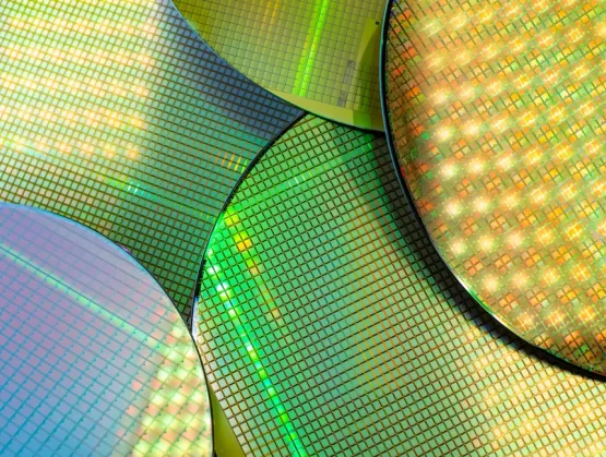
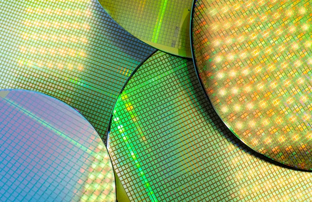
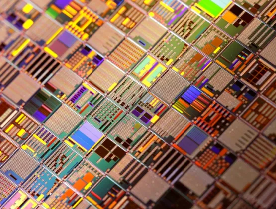
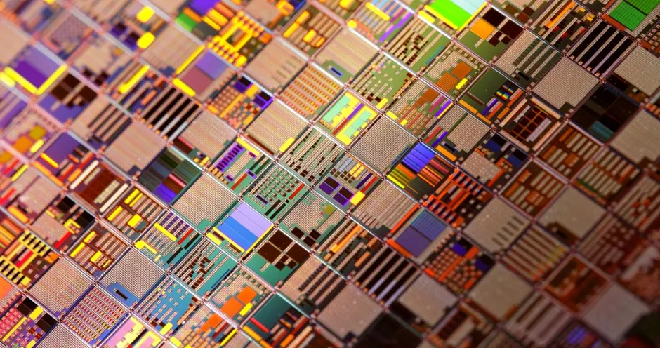
downloadGroupGroupnoun_press release_995423_000000 copyGroupnoun_Feed_96767_000000Group 19noun_pictures_1817522_000000Member company iconResource item iconStore item iconGroup 19Group 19noun_Photo_2085192_000000 Copynoun_presentation_2096081_000000Group 19Group Copy 7noun_webinar_692730_000000Path
Skip to main content
Default Banner Image

ESD Alliance

Today’s post is the last of four Q A-style feature posts based on presentations during SEMICON West 2025’s “The Convergence of Semiconductor Manufacturing and Design” organized by the ESD Alliance (ESDA).Bob Smith interviewed Joe Kwan, Director of Product Management from Siemens EDA, about his presentation, “3D Design Brings Multi-physics Requirements While Manufacturing Yield Improvements Require Digital Twin Modeling and Ingesting Design Data.” They covered a range of topics from partner collaboration and integrated design flows to digital twins, AI and more.Smith: How does Siemens EDA define collaboration between design and manufacturing? What does that look like?Kwan: Manufacturers and designers have been cooperating for a long time. The most familiar example is the design rule check (DRC) rule deck provided by the foundry to the design team. It enforces designers to adhere to the layout rules that must be followed for a design to be manufacturable. What’s different now are new problems arising from the latest advances in technologies. Close collaboration is needed between the design team and foundry to identify and share data necessary for a successful final product. Foundries are challenged to encapsulate information that provides design teams with critical information for success without divulging proprietary data.Smith: Can you elaborate with a few examples of what technologies you are referring to that are driving these new collaborations?Kwan: Sure. A great example is the industry’s move from monolithic single chip solutions to chiplet-based solutions that require 2.5D, 3DICs, heterogeneous integration and the like. These approaches require multi-physics simulations to verify physical phenomena in ways that were not necessary when previously focusing on just a single chip design. Thermal, electrical and stress are not independent variables anymore.Design teams need to understand how these effects come in to play with functionality, performance and other design specifications. Most important, they need to be aware of factors that could cause the chip or system to fail. To do this, close collaboration between all parties involved (design team, foundry and packaging) is required so designers know what to look for in their analyses and what to avoid. It adds a whole new layer of complexity necessary for getting to the finish line.Smith: I imagine some scenarios that fit into what you are talking about. For example, if the design includes stacked die, the team will need to be concerned about heat distribution and potential hot spots in the stack. Kwan: That is a good example. Heating problems cannot be overlooked. How does the heat escape from the stack? What is the thermal profile across the stack from the die on the top all the way through to the bottom of the stack. Is there a sufficient pathway for heat to get out? We can do rough estimates early on to see if putting this die on top of this other one, is it going to work? Or be reliable? Back of the envelope calculations might show that the dies need to be positioned differently or even designed differently. Smith: What can be done to improve design success?Kwan: This is where collaboration comes in. The product owner should establish a cross-domain team of experts from chip design, package engineering and process engineering. The product spec and design decision trade-offs must be evaluated against impact to all domains.EDA also plays a critical role. EDA is the link between designers, packaging and manufacturing. We hear and capture concerns from designers and package engineers. We prototype solutions, collaborating with packaging and IC manufacturers to encapsulate requirements for successful production.Smith: At SEMICON West, we also talked about how design data can help foundries during the manufacturing flow.Kwan: Yes, going back to our discussion at SEMICON West, I spoke about that important topic, which is embodying design data into the manufacturing platform in the context of a digital twin for virtual metrology.In an ideal world, we would measure everything. If we could do that, we would have all the data needed to make perfect manufacturing decisions. But it would be extremely expensive. What we can do instead is apply AI virtual metrology. We collect the usual sparse metrology and then combine design data to train a predictive engine. The result is the ability to accurately predict where metrology was not collected.With traditional process-of-record, foundries run a qualification wafer every 10 or so wafers. That’s very expensive. With virtual metrology, we can predict when drift becomes significant enough to blow up a wafer and you can intervene to restore individual nominal tool performance.Smith: Engineers are writing their own agents to automate parts of the design flow such as analyzing the outputs of simulations.Kwan: We see a lot of interest in AI and Agentic AI. There is a lot of potential to improve engineering productivity. But as we race to develop Agentic AI flows, we must also approach this in a rigorous manner that cross-checks to ensure accurate and robust results.About Joe Kwan Joe Kwan is the Product Director for Calibre AI/ML Fab Solutions at Siemens EDA. He has more than 30 years of experience in the EDA semiconductor industry. He previously worked at VLSI Technology Inc, COMPASS Design Automation, Silicon Access Networks and Virtual Silicon. Kwan received a Master of Science degree in Electrical Engineering from Stanford University and a Bachelor of Science degree in Computer Science from the University of California, Berkeley. Robert (Bob) Smith is an independent consultant who has been involved directly in multiple roles in the EDA industry over the past 38 years. His career experience spans analog engineering, marketing, sales, business and strategy development and others including numerous c-suite roles. He holds a Master of Science degree in Electrical Engineering from Stanford University.
Read More
Lu Dai, Vice President of Technical Standards at Qualcomm, presented “Converging Chip Design and Manufacturing in the Era of High Integration” at SEMICON West in October 2025, offering an insightful look at how design and manufacturing are collaborating effectively.I had an opportunity to talk at length with Dai and asked him to define collaboration. His thoughtful answers, perspective on industry trends and what it will take for a seamless automated flow between design and manufacturing made for a great discussion.In addition to his role at Qualcomm, Dai, who lives in San Diego, is Chairman of Accellera Systems Initiative, Chairman of RISC-V International and Director of Silicon Integration Initiative (Si2).Smith: Qualcomm is a fabless company. How do you define what collaboration is between design and manufacturing? Dai: When we talk about design and manufacturing collaboration, we need to consider how a design is optimized for a certain manufacturing process. For example, will an advanced manufacturing capability help designers simplify designs or allow them to bypass traditional actions?I compare it to the way software was optimized to hardware because of hardware limitations. We had to make sure the C code was compact and that the variable types we specified wouldn’t waste memory. We also had to write the code in a certain sequence to speed up the execution of the code. As hardware capability grows, we can write dirty code and it isn’t as critical. We understand the manufacturing process capability. That allows us to be more flexible about where to focus the chip design effort based on needs for power, performance, area, and schedule. We want to make sure we know the chip size and how big the silicon space is for certain features. For example, low power is often a key feature of today's designs. As manufacturing process nodes improve, power goes down and area shrinks. We can therefore focus more on optimizing performance.This is the kind of collaboration we use with foundries. Libraries need to be optimized for the design and tweaked for yield. This collaboration is critical for foundries pushing leading-edge nodes in the design house—they have to work closely with the design team.Smith: And how about collaboration with packaging suppliers? Dai: I'm not a packaging expert. Traditionally, packaging is one of the important steps and even more so because of the push toward the use of chiplets. Packaging becomes really important when dealing with multi-chiplet types of design. Traditionally, IP vendors sell a license to use the register transfer level (RTL) code, which is subject to IP theft. With a chiplet approach, they sell a netlist, which often becomes a hard coded chip as a bundled service instead of a single IP. The subsystem sales approach makes more money, creating another opportunity or a new landscape. SoC companies may get into the IP business and conversely, IP companies are getting into the SoC business by selling the bundled subsystem. Smith: The margins are getting blurred. It sounds like there is collaboration and it’s between designers, but also the foundries, process and the packaging.Dai: And partially between EDA tools because both the design side and the manufacturing side are speaking two different languages. EDA is somewhere in between, helping the translation.Smith: What are the trends and challenges that make it hard or even prevent a fully integrated flow?Dai: The extremely high costs of doing the implementation for an advanced node, especially for the first tape out. If we are the first to use the newest node, we know there is a tremendous benefit in the long run. But we are also the pioneers that have to work out the tough challenges. Few companies have the technical capability and deep financial resources to be the pioneers for a new process node. We’re starting to see high-flying semiconductor companies use leading-edge nodes. On the design side, they are challenged and trying to run faster by adopting a newer node. Cost is probably the biggest challenge for this collaboration. If their margins get challenged or they need to be a little bit more careful, they adapt by becoming fast followers.Another challenge comes from more specialized designs. There has been a long period where general-purpose chips are used for many different applications. But, we are now seeing designers increasingly focus on more specialized chips with custom designs.Custom IP and ASICs are becoming trendy. Designers are trying to figure out how to make a general baseline and then differentiate on certain IP and the best possible manufacturing process for the application. Doing a custom chip on an advanced node is quite expensive. We may be challenged if we don’t have sufficient data to clean up a process because every chip and process combination is unique. Lessons learned from this chip may or may not apply to everyone, while a general-purpose design tends to be a good baseline for lessons learned.Smith: How do you envision an integrated automated flow between design and manufacturing? Dai: In today's environment, we would like an RTL design to be fully portable to any kind of manufacturing process or foundry. Based on our architectural and business, we could then pick and choose the fab and the process. How do we port a design into a new process? That's difficult because we need to consider special constraints required by the new process that didn’t apply to the previous process. There's also the reverse case for porting a new design into an old process.Let’s say we have a chip designed for a 3-nanometer process and we want to port it back to a 28-nanometer process. Why would we want to do this? Imagine a COVID type of situation—a supply chain constraint and/or a geopolitical flare up with no access to the advanced fab, but an older local fab is still available. In this case, we need the chip for the feature it provides. Perhaps a car needs that chip and it was designed to be produced in a three-nanometer process but is suddenly unavailable. A 28-nanometer chip that runs at half of the speed might do the job for a few years. Unfortunately, this is somewhat wishful thinking because of the challenge of the flow. We didn’t think about it but we have to do it now and need to consider whether we have sufficient time to work out the challenges.Smith: How do you make that decision for making chiplets? Dai: Porting to another process is not a small job. It's labor intensive going from a same design in one process to another process.The project lead presents a process porting non-recurring engineering (NRE) cost budget to management. The questions span resources and time needed that boil down to how much money will need to be invested to achieve the porting. It should be simple. It’s not. It’s a lot of work.For many companies, the strategy is to offload the porting to a low-cost geographical team with a cheaper NRE that matches management expectations for the costs of process porting. History often shows that the company is not reducing that much time and manpower by offloading the porting. Smith: What about the EDA tool side? Is there typically a team from the EDA vendor? Dai: For advanced nodes, we involve the EDA and in-house EDA experts when certain parts of our design don't work out as expected.Back-end tools need experts involved in the debugging. And if we don't have an in-house expert, we need our EDA vendors to send engineers to work on the project.Smith: I have a generic question about AI. We talked about reporting. Where would it fit in collaboration?Dai: Sooner or later, we're going to be asked for a proper supply chain tracking or hardware bill of materials (BOM). Conceptually easy, but difficult in practice because it goes from logic design to physical design all the way to manufacturing. How do we carry that type of information through each step with EDA tool providers and manufacturing equipment providers? Their credentials need to be registered and they can’t alter any of the existing flow credentials.Supply chain tracking can ensure that if there's any kind of natural disaster or geopolitical issues, the hardware BOM is properly categorized, and the chip can be made. Security is another reason for supply chain tracking. Collaboration between design and manufacturing is important because once a netlist is sent to the foundry, our job is to make sure it is done correctly. We wait for our silicon to come back. Then we do testing. But during manufacturing, the chip comes back and it doesn't work. How do we know if somebody tampered with it? Supply chain tracking could help.Smith: How can you know that someone didn’t tamper with a chip design after it was handed off to manufacturing? This could cause big issues for end markets such as medical, automotive, defense and aerospace applications.Dai: The solution is EDA heavy because EDA tooling can help on the traceability at every step. It’s all automated through some kind of tool. If we need to have a proper format, we need to have proper encryption. And we know when we use this tool to run it, we check to show we are using the real tool not a hacked version that doesn't have the security credentials.Smith: Will this drive supply chain tracking or drive new standards?Dai: I hope so. Once upon a time, there was an initiative by the Department of Defense to track the supply chain. It was a mandate and no one liked it. It’s much better for the industry to proactively come up with a standard for a global economy.A mandate tends to come from one government. It may be a good mandate if we do business only within one country or within a small region. What if we have to do business with another government that may not like our mandate? Say a certain part of our design stage is done in a different country and we need this level of detail. Who's doing the work and what's the tool version? Per local government rule they may not be willing to give the information to us. This might be sufficient. We don't know the details of the risk, but we know there is a risk. We could simply add to our tracking that a portion of design is done in a foreign country with foreign EDA. It's important to have an industry standard and an international standard so that we can procure our tools and the services around the world instead of being limited.Smith: How can we encourage companies and people to want to cooperate and sign on to a project like this?Dai: With lessons learned, we can go deeper. Maybe the first level is a meeting in the U.S. About Lu DaiLu Dai is Vice President of Technical Standards at Qualcomm Technologies, Inc., spearheading semiconductor standards efforts and relationships with industry organizations. Lu was previously Senior Director of Engineering and led Qualcomm’s SoC design verification team and front-end methodologies and initiatives. He was also the Design Verification Lead responsible for multiple generations of premium tier platforms at Qualcomm, including the Snapdragon 8 series and products that power the Mars Perseverance rover and Ingenuity helicopter. Prior to Qualcomm, Lu was the Design Verification Lead for Cisco’s Gigabit Switching Business Unit where he worked on multiple generations of Cat4k ASICs. Lu is the current Chair of Accellera, Chairman of the RISC-V International Board of Directors and serves on the Board of Directors at Si2. Lu holds a Master of Science degree in Electrical Engineering from Cornell, and a Bachelor of Science in Electrical Engineering and Computer Science from UC Berkeley.Robert (Bob) Smith is an independent consultant who has been involved directly in multiple roles in the EDA industry over the past 38 years. His career experience spans analog engineering, marketing, sales, business and strategy development and others including numerous c-suite roles. He holds a Master of Science degree in Electrical Engineering from Stanford University.
Read More
Ann Wu is CEO of EDA startup Silimate, developer of a co-pilot (chat-based GenAI) for chip and IP designers to find and fix functional and power, performance and area (PPA) issues in their designs. Rick Carlson is Vice President of Sales at ESD Alliance member company Verific Design Automation, provider of front-end EDA platforms to a range of small and emerging EDA companies like Silimate and larger EDA vendors.I recently talked with Ann and Rick who represent EDA’s new and old guard. I found them to be bullish about the emerging EDA space called AI EDA that uses GenAI and large language models as the foundational tools and the swelling numbers of well-funded startups entering this space.Smith: Ann, you were an Apple hardware designer. What encouraged you to leap into entrepreneurship using AI as the foundational technology?Wu: It was always my goal. Apple afforded me the opportunity to understand how one of the best companies producing some of the most cutting-edge chips in the world operates. It also gave me the opportunity to work with some of the most brilliant engineers and operators. My plan was then to go back to Stanford to explore and start a compelling venture with another similarly motivated friend, Akash Levy. That was the genesis of Silimate. The drive for leaping into entrepreneurship then ultimately stemmed from my frustrations with the existing chip design process. I sensed there was an opportunity to apply AI technology to solve some of these limitations of the existing approaches to chip design.Smith: What made you think that AI would be applicable to the EDA challenges that designers face?Wu: AI provides a compelling solution to some of the intractable problems that have existed in EDA. Traditional EDA solutions solve isolated problems through heuristic algorithms. There’s a high volume of gray area between the well-defined boxes of inputs and outputs that had previously been unsolvable. Now with AI, there is finally a way to sift through and glean patterns, insights, and actions from these gray areas.That’s the macro reason why there's so much excitement and appetite around the application of AI for EDA.Smith: It sounds like productivity enhancement. What are some other key words or selling points to use to convince a designer of AI’s potential for EDA?Wu: I would say "speedup" is one of those keywords. Ultimately, the designer is trying to meet or even shorten the time to tape out while hitting their design spec. That's driving all decisions, whether to throw more headcount at closing a certain block or to defeature something that's going to cause the team to miss the shuttle. It all comes down to whether a fully featured and functional design gets to tape out and gets to market ahead of competitors.Productivity as a keyword is not compelling. It’s hard to translate how saving minutes or hours of an engineer's time connects back to the bottom line. The bottom-line decisions are driven by the project’s timeline as time to market is everything.What’s needed is a way to sift out and resolve real design problems 100x faster, which ultimately results in real speed up on a project’s schedule. For example, processing large amounts of data with AI to find issues actively helps the designer converge their design to their target.Finding and resolving issues in a design within minutes instead of days or weeks instead of months is the kind of impact that directors, VPs, and managers want for adopting new tools.Smith: What is driving hardware designers into this EDA space?Carlson: The thing that's most intriguing is large language models, neural networks and AI. It seems like an “aha” moment when startup founders believe they can do something that's dramatic for the first time.When I look back over my photobook of moments in my time in the EDA industry, there's the wonderment. The things that can be brought to bear with iterative versions of new technology from companies like Ann's will offer multiple “aha” moments. This is game changing.Smith: Are venture capitalists investing in EDA again?Carlson: Yes. Some venture capitalists haven't invested in EDA for decades. These are smart people. They have plenty of good people that can do good due diligence. The amount of money that's being invested is significant. It's not just a little bit of seed funding. One startup’s first round was $3 million. They're now raising $20 million in the next round. They're saying that their pre-money has to be $50-$60 million. They're just coming out and there's a huge amount of interest.We're going to be looking back in a year and say we just couldn't believe how much money is pouring into this. It has a huge impact on the world stage. This is an amazing time to be doing anything in and around the design of computer chips.Smith: Y Combinator (YC) invested in Silimate.Wu: Yes, that's right. It's an honor to be the first EDA company that YC had invested in. The semiconductor and EDA space had been under the radar until recently—it’s such a critical piece of our technical infrastructure. The semiconductor industry hasn't been headline news in past years. Now every other day, the Wall Street Journal runs some semiconductor chip-related article. People are realizing this is a fundamental piece of our world's tech stack, and the software that drives this tech stack is equally important and there are investments to be made.Learn more about Verific and Silimate during the 62nd Design Automation Conference (DAC).Verific will exhibit in Booth #1316 at the Moscone Center in San Francisco from June 23-25.Silimate’s Akash Levy, Founder and CTO, will participate in a panel titled “AI-Enabled EDA for Chip Design” at 10:30am on Tuesday, June 24, 2025.Robert (Bob) Smith is executive director of the ESD Alliance, a SEMI Technology Community.
Read More
In an era where technology permeates every aspect of our lives, the semiconductor industry serves as the backbone of innovation. From IoT devices to data centers, every piece of technology relies on integrated circuits (ICs) such as intellectual property (IP) cores and system on chips (SoCs). As these technologies become increasingly pervasive, the importance of hardware security assurance in the design and development of IP and SoCs cannot be overstated. Evolving cyber threats and sophisticated attacks make it essential for vendors to integrate advanced security measures into their workflows.Market Pressures Driving Demand for Enhanced Hardware Security The semiconductor market is projected to reach $1 trillion by 2030. At the same time, semiconductor devices and system designs are becoming increasingly complex. With that complexity comes the added difficulty and effort required to conduct thorough security analyses. Additionally, competitive pressure to reduce time-to-market means that vulnerabilities can be more easily overlooked or exploited, making it crucial for the industry to adopt automated security solutions. As more products are deployed in critical systems, from consumer electronics to national infrastructure, the stakes become even higher, underscoring the necessity for robust security measures.According to the SEMI Electronic Design Market Data (EDMD) report, in 2023, the electronic design automation (EDA), semiconductor IP, and related services market reached $17.1 billion, fueled by the increasing complexity of semiconductor designs and the growing emphasis on security. While the overall EDA market is growing at a 7.4% compound annual growth rate (CAGR), the semiconductor IP segment is expanding at 9.7%, and in comparison, the logic verification tools market alone is surging ahead at 24.2%. Deeper verification processes and tools are needed to not only handle the rising complexity of semiconductor designs, but also to support the growing emphasis on secure-by-design principles to ensure robust and reliable products in an evolving technological, security, and threat landscape. As a result, the market for logic verification tools — a key component of the EDA market — is surging. The Rising Cost of Cyber Threats from Data Breaches and Architectural Flaws Pavani Jella, Silicon AssuranceThe average cost of a data breach is $4.88 million1, encompassing lost business, regulatory fines, legal fees, and damage to brand reputation. As the semiconductor market grows, the potential financial impact of security breaches due to hardware vulnerabilities also escalates. Companies must invest in robust security measures to mitigate these risks and protect their financial health.Cyber threats from the exploitation of architectural flaws are another threat. Plundervolt is one example of an architectural flaw that could lead to hardware exploitation. Discovered by ethical hackers, Plundervolt is the name of an attack that exploited voltage fault injection to compromise the security of Intel processors. By manipulating the voltage supplied to the CPU cores, attackers could induce errors in the SGX enclave, allowing them to leak sensitive data or even bypass security protections intended by the enclave. This flaw was particularly concerning because it operated at the hardware level, making traditional software security measures ineffective. The attack leveraged the SoCs’ power management features, specifically dynamic voltage and frequency scaling (DVFS), to achieve its malicious objectives.Exploiting such a vulnerability could lead to the exposure of sensitive data, such as cryptographic keys and proprietary information, compromising the confidentiality of secure enclaves. This breach could erode trust in an IP or SoC provider’s security features, particularly in environments that rely on using the IP or SoC for protecting critical data. In cloud environments, a successful exploit could result in multi-tenant data breaches, impacting numerous users.The vulnerability also poses risks to secure applications, potentially leading to manipulated outcomes and decrypted communications. Businesses could face significant financial losses, operational disruptions, and regulatory consequences due to such an attack. It is a stark reminder of how architectural flaws in SoCs can be exploited, leading to severe security breaches that are challenging to mitigate without hardware-level fixes.Industry Believes Hardware Security Assurance Is a Key Priority A majority of security professionals from a diverse group across industry, defense, government, and academia rate hardware Trojan detection, IP piracy protection, and SoC vulnerability assessment as high priorities. This prioritization reflects the industry's awareness of the critical importance of security measures in maintaining the integrity and reliability of semiconductor products.As a result of this awareness, investments in cybersecurity are expected to reach $345.4 billion by 2026, growing at a CAGR of 9.7%2. This substantial investment demonstrates the global commitment to enhancing security measures across all industries, including semiconductors, to combat the escalating threat landscape.New EDA Tools and Investments Needed to Combat Cyber Threats The adoption of new EDA solutions is essential, despite the initial costs. Costs can range from $100,000 to $1 million per license for general EDA design and verification tools, depending on the complexity and capabilities of the software. Pre-silicon security EDA tools can detect vulnerabilities early in the design phase, significantly reducing the risk of exploitation and the need for costly post-production fixes while enhancing product reliability. Secure-by-design principles ensure that security measures are integrated throughout the development process, rather than added as afterthoughts.Integrating these new tools also requires investment in training and potential adjustments to existing workflows. However, the improved security and efficiency provided by these tools can offset these initial costs.While the costs of acquiring advanced EDA tools and deploying them in the workflow is significant, the investment is justified by the long-term benefits of enhanced security and reduced risk of costly breaches. Secure-by-design practices can prevent significant financial losses from security breaches, offering substantial long-term savings. Companies that invest in robust security measures are better positioned to demonstrate market leadership and build customer trust and loyalty, while avoiding the reputational and financial damage associated with breaches.ConclusionThe semiconductor industry is at a critical juncture where the application of advanced EDA solutions for hardware security is not just beneficial, but essential. The time to act is now.The increasing sophistication of cyber threats and the financial repercussions of security breaches make it imperative for IP and SoC vendors to adopt advanced EDA security assurance solutions to secure their designs. By investing in cutting-edge EDA tools and prioritizing security from the earliest stages of design, vendors can safeguard their products, maintain market competitiveness, and protect against the ever-evolving landscape of cyber threats.References1. IBM Cost of a Data Breach Report 20242. KPMG 2024 Global Semiconductor Industry OutlookPavani Jella is the Vice President of Business Development at Silicon Assurance, a member of the Electronic System Design Alliance (ESDA) a SEMI Technology Community. Silicon Assurance specializes in hardware security assurance solutions. With a strong background in the semiconductor and EDA industries, Pavani plays a pivotal role in driving strategic growth and fostering innovative partnerships. Passionate about the intersection of technology and security, she helps organizations adopt state-of-the-art solutions that ensure the resilience and trustworthiness of their hardware systems.
Read More
Executive Advisor Jeff Lewis held the position of Vice President of Marketing and Business Development for Artisan Components, one of the early companies developing blocks of intellectual property. Lewis, who worked at Artisan from 1996-2000, and his colleagues were members of an elite group who built the mega-successful IP market, estimated today at $7.48 billion. Arm acquired Artisan Components in 2004 for $913 million.In my role as Executive Director of ESD Alliance and publisher of the quarterly Electronic Design Market Data (EDMD) report that includes IP, I recently talked with Lewis about what he remembers from the early days of IP.Smith: You were part of the IP revolution. What were the high points and low points that you most remember? Lewis: The high point was starting with a relatively blank slate and innovating. Some things worked, some didn't. We kept trying different things and seeing what would work with plenty of failed tries, successes, and repeats. We got a chance to be on the ground floor of a new industry. Another high point was watching this nascent industry emerge into a powerhouse. In the ‘90s, EDAC (Electronic Design Automation Consortium, the predecessor to the ESD Alliance) wasn't interested in tracking IP. As the IP market started growing, EDAC was all over it because it helped pump up the size of the electronic design automation (EDA) industry. Suddenly, IP had become a big enough industry that people were starting to care. And of course, there were successful public companies like Arm, Rambus, Artisan, and others licensing IP. It was fun being part of that.The low points were the hard part. While everything was new for us, it was also new for customers. They had intense resistance to licensing IP that many viewed as product development. They would want the IP company to develop something under a consulting or NRE contract, and then they would own the product and all the IP around it. They wanted to own everything. Many companies had that mentality in the early days and were resistant to licensing or paying royalties.As a side note, Gary Smith, former analyst for Dataquest, now Gartner Group, who died in 2015, and I had an ongoing debate. We went to lunch quite frequently and he would say, “IP is great, but you aren't IP. You are a standard cell, and it is not IP.” It was one of his standard statements.He would make various presentations, and I would argue: “You can't think of it as a cell, think of it as an entire library. It's an entire library with all the design views, layouts, test and qualification data, and everything else. That’s intellectual property. Plenty of intellectual property goes into developing it.”He eventually changed his mind and agreed when he saw the revenue and the value –– IP companies do it better and cheaper than in-house development.A final high point was getting the idea and value of IP across to customers. Smith: At what point did people start to believe IP was a real market and they could trust a vendor? Lewis: I don't know if there was an inflection point. More and more people started getting used to the idea that IP was an industry. Arm was probably the major catalyst. Artisan had two different engagement models. One was the integrated device manufacturer (IDM) model. Mark Templeton, co-founder and CEO of Artisan who died in 2016, and Lucio Lanza, Managing Partner of Lanza techVentures and Artisan’s Chairman, are credited with developing the royalty model and the intellectual property category. They drove it with the IDM model. Executive Advisor Jeff LewisCustomers knew they were paying for a license, understood the terms and became both the licenser and the user of this technology. It was different when Artisan went to the foundry model, which extended the IDM model to the rapidly growing foundry space. In this model, Artisan had the ability to widely disseminate its IP to all the foundry customers for free. However, calling it a “free library” is a misnomer, because often overlooked in this process is that the foundry paid up front for every one of those libraries, and it also paid a royalty on each design that used them. Artisan was profitable from day one by building a library or memory compiler. The engagement model was one where Artisan could proliferate these to the foundry’s users. They would get the library, and the royalty would come from the foundry. Users were beneficiaries – they had a simple license agreement, but unless they needed some customization, they weren't writing checks to Artisan.From the user’s perspective, it was great. They got free libraries and IP. That helped open people’s eyes to the model that could be a good thing. Artisan had 1,000 users at one point, and it helped drive the proliferation of IP use in the industry.Smith: Is that foundry model still in place? Lewis: Largely, yes, with some exceptions because foundries have a standard library that can be used. They have some specialized IP that customers license. While there are variations, foundries provide libraries to their customers. TSMC has engineers developing libraries for its own processes. For a long time, Artisan was the standard IP provider for most of the foundries. Smith: How did companies overcome verifying and testing IP? Were engineers skeptical about buying from an unknown/unproven company? Lewis: This is an important and critical question. Engineers were skeptical about buying from an unknown or unproven company. Artisan’s library quality was our biggest selling point, and it was the same with Arm and Rambus. Size and reputation were a huge advantage.The key was to have a major win that demonstrated your bona fides, and our biggest early win was our work on the Sony PlayStation. At that time, LSI Logic was developing the chips for the PlayStation, but was looking to outsource some of the critical blocks, such as the embedded SRAMs. Sony engineers were nervous and wanted to meet the IP companies to see what they were doing, because the fate of their chip was resting on these little companies. Artisan developed high-performance embedded SRAMs that replaced the existing LSI SRAMs. Our memories were about half the size of the LSI SRAMs, higher performance, and worked the first time.What’s instructive is how Artisan later got the foundry relationships going and sold libraries. Enabling first-time success is a quality argument, because the design would work the first time. At that time, almost every foundry library had bugs in them that caused silicon failures after tape-out. Our primary argument to engage foundries was our impeccable QA story. We had customer testimonials confirming that the foundries would not have library-related failures. When foundries scheduled a volume like a PlayStation ramp, they couldn’t afford a production “bubble” or “hole” in their production schedule from a library bug causing a chip not to work and requiring a re-spin.That's why the argument on quality and first-time success was critical to TSMC.One more thing on quality, and this ties specifically to Artisan and almost all IP companies. Any company that focuses on a mass proliferation model must ensure their product has no quality problems. Mass proliferation needs to be as low touch as possible, so engineers can use it without constantly calling for support. Quality is an absolute fundamental before mass distribution, because the fastest way to go bankrupt is to massively proliferate a faulty product. Smith: According to the EDMD report two years ago, IP surpassed front-end EDA tools as the highest category. Are we now shifting into a world where IP in the form of chiplets may become the dominant player? Lewis: I think the shift is coming. These are different incarnations of Moore's Law and the Carver Mead-structured VLSI. Sometimes the structure may be a chiplet, or the structure may be embedded.Is it virtual or is it actual? Engineers will make tradeoffs with pros and cons of embedding it or keeping it separate. The deciding factor is which silicon process is best and how it will be implemented. The SEMI EDMD report’s tracking of the Semiconductor Intellectual Property (SIP) and its rise to one of the market’s leading category. Smith: You worked for several IP companies that were offering process-related IP. That's a completely different type of market selling cycle, correct? Lewis: It is, because I focused on technology licenses for manufacturing processes, as opposed to the much more understood design IP that was developed for the existing manufacturing processes. Getting inserted into a company’s manufacturing process is much more difficult and challenging.If a company is licensing a technology that modifies the front-end process, then the process parameters will change, presumably for the better. The re-optimization can be like whack-a-mole. While some parameters get better, some may get worse, and further re-optimization can be required. This can go through several cycles until the process converges. This also means that all existing IP must be recharacterized and/or redesigned, which is why it is best to insert a new technology at the beginning of the node development rather than as a retrofit.Adding new process technologies is inherently difficult unless it’s a separable piece. For example, many new memories such as ReRAM or MRAM are licensed technology and separable, because they are set up separately in the metal stack. They don't touch the transistors.For a long time now, companies have been able to pick and choose whether to do in-house development or procure design IP from a third party. We're now starting to see the same thing in process development, because they are getting so complex, and no one can be an expert in all areas. I see process IP as paralleling the early days of design IP, but with a 30-year delay. Back then, most customers were reluctant to procure design IP because they felt: “We can do it all in-house.” Almost no one says that today, and I think this gradual acceptance will apply to process IP as well.Smith: Should Mark Templeton be considered the innovator and creator of the IP industry? Lewis: I’m not sure there’s anything I can say about him that hasn’t been said already. He was a great guy and an important thinker. I credit him for doing an excellent job crafting a successful company. And, of course, Lucio Lanza was absolutely instrumental as well. He pushed Artisan to do royalties, and Mark helped drive it to fruition.About Jeff LewisJeff Lewis is one of the pioneers of the semiconductor IP industry, participating since its inception in the mid-1990s. Lewis is currently Executive Advisor for senior management and investors for semiconductor and AI companies. He was previously an operating executive serving as Senior Vice President of Business Development and Marketing at Atomera Incorporated, Spin Transfer Technologies, SuVolta Inc., and Innovative Silicon Technologies, and held operating roles at Synopsys, VLSI Technology, and HP. Lewis earned an MBA from the UC Berkeley Haas School of Business, and has a bachelor’s degree in electrical engineering, and a bachelor’s degree in economics from UC Berkeley.Robert (Bob) Smith is Executive Director of the ESD Alliance, a SEMI Technology Community.
Read More
John Kibarian, CEO and founder of PDF Solutions and a member of the ESD Alliance (ESDA) Governing Council, is a keen observer of the semiconductor ecosystem. Since PDF Solutions sits between design and manufacturing, Kibarian shared unique perspectives on both in a recent discussion.Smith: What trends are you seeing in the semiconductor industry. Are there any that surprise you? Kibarian: We see several trends that have been going on for quite a while.As much as we hear Moore’s Law is dead, there's still a strong drive to get to advanced nodes. The benefits are harder to achieve and require more than geometry scaling, but demand for these advanced nodes continues to grow. Another emerging trend is the need for insatiable compute power in data centers to support the explosion in AI applications. In recent history, the mobile phone market has been the key driver of the push to new advanced nodes, but that is changing as the performance needs of data centers and AI applications are now driving the shift.Next, as companies are still learning from the disruptions in the supply chain due to the pandemic, there’s a tremendous amount of movement to make the supply chain more resilient by expanding sourcing options for critical products or test applications. This is happening in conjunction with significant investment in high-performance compute from many countries that want to bring silicon to their shores.The next trend is that electronics companies are looking to limit investing solely in China or the U.S. Their China Plus One or U.S. Plus One strategies results in adding significant additional infrastructure and overhead. If it's not done right, it will cost the industry more money. It will be hard to sustain the cost benefits and economies of scale of the current single source model just by brute force and adding human capital. A new approach is required to manage cost effectively smaller and globally distributed manufacturing facilities.The final trend is the general electrification of the economy. Cars are moving from internal combustion engines to electric. That means more and more of our energy needs are met with electricity, putting a premium on solar and batteries. Batteries require power conversion.Silicon such as high bandwidth semiconductors on silicon carbide and gallium nitride have a tremendous amount of capacity. What is interesting is how fast and aggressive China is in that part of the market; they could be a major producer of the technologies needed to support electrification. With our exposure to the China market as well as the European and U.S. markets, Chinese manufacturers have come up quickly, and we may see a world with more viable suppliers than originally anticipated.Smith: You mentioned data centers and AI. AI is everywhere and revolutionizing the semiconductor industry. EDA companies are talking about incorporating AI. What are you observing? Kibarian: AI is used for chips that are manufactured for use in data centers. For example, our customers use PDF analytics or the Exensio platform via the cloud to analyze large amount of manufacturing data and product or test engineering data. Without this type of automated solution, only a small proportion of these data sets would actually be utilized.Companies staff their product design and test engineering using a budget based on a percentage of revenue. If a company has billions of dollars of revenue, it will put so much more into product and test engineering. But how productive can these people be? Without AI, they can only use some simple reports and graphics to analyze the subset of data they are looking at. AI solutions such as PDF’s Guided Analytics capability apply sophisticated machine learning tools to analyze entire large data sets. AI is enabling engineers to be more productive by allowing them to work with large data sets that ultimately deliver better results in the products.The amount of compute keeps going up at a rate that outpaced the rate of geometric scaling. More compute power makes it cost effective to go through large data sets and identify what is relevant.Additionally, AI is helping semiconductor companies build products. A conventional compute system is chips assembled on boards. AI is making system-in-package take off.The production flow is more complex, as fabless companies are becoming system companies. Conversely, system companies are becoming fabless companies and manufacturers. In the past, they ordered parts from their foundry of choice. Essentially, the foundry was the system manufacturer, supplying package and test yields of 99%.Now companies are building systems in more complex packages potentially with foundry partners, but this requires getting known good die. High bandwidth memory or other components from other suppliers means the company must make sure these products are available at the right time. In essence, they are becoming manufacturers and changing the way customers manage the problem of product test. They're adding more test insertion points and using machine learning and AI to be more productive.Smith: Let’s talk about digital twins or creating virtual models of everything from chips to the whole system. How do you see the impact or effectiveness of digital twins in manufacturing? Kibarian: From a manufacturing perspective, digital twins had been models for chamber behavior on a processing tool like an etch tool or TCAD simulation of devices and structures.The problem is that purely physics-based digital twins don't exist, and we must utilize empirical data. The joke was that the modeling for tomorrow’s systems was based on yesterday's technology. Trying to have the physics catch up with the materials, device structures and behaviors is why it’s so expensive to develop new technology.Principles-based models will never catch up with production. We can model 90-nanometer technology, but it doesn’t work for one or two nanometer wafers. AI and machine learning – and ways of building models using more sophisticated algorithms – can help close that chasm, and that’s starting to happen at the R D level.In production, no one has yet achieved a good merger of the physics-based and AI-modeling worlds to create a virtual model. Virtual modeling is a big opportunity.The rate of change and improvement in algorithms in large language models moves fast because machine learning can scrape the Internet for data to build huge training sets. In the semiconductor world, however, data sources are typically siloed within organizations and often not shared with vendors. This limits the rate at which the industry can take full advantage of existing data and create tangible economic benefit.By and large, there is a lot of wasted capacity in semiconductor manufacturing. The operational effectiveness of factory equipment is up to 90-95%. The reality is that most factories today process product wafers 40-60% of the time – maybe 70-75% of the time on a test floor. It is critical for the industry to start leveraging new types of AI models to increase the productivity of its manufacturing capacity.The industry needs to look at how companies can share data to take advantage of more sophisticated AI and create a new kind of operational digital twins. If the industry doesn't make a change; it will only be the largest facilities with the largest datasets able to take advantage, leaving one or two winners, with the others not being competitive.Smith: Is it possible for the industry to come up with a standard or some way of sharing information to build better models without giving away the underlying proprietary data? Kibarian: We can look at computer science with technology like homomorphic encryption. The relationships between parameters remain, but the underlying numbers or raw data is not visible after encryption. Pharma and the medical industry have ways to add noise to the data while preserving the information, as required by the Health Insurance Portability and Accountability Act (HIPAA).Our industry has a knee jerk reaction when it comes to looking at how to take full advantage of data and prefers to solve it as if information and data is more proprietary than medical data or financial data. And I don't think that’s true.Bob Smith: Is the open-source movement destined to bring change to the industry? Kibarian: PDF is a big believer in open source when it comes to OS-level virtualization and Kubernetes versus proprietary alternatives. We also use open-source database technology like Cassandra but are skeptical of the value of open-source solutions for end-market verticals. Having an underlying open and available IT layer has tremendous value, because it means a more rapid rate of innovation and greater ability to adjust security vulnerabilities and patches versus proprietary systems.Smith: PDF sits right between manufacturing and design. On the EDA side, more collaboration is going on between designers and manufacturing. How would you bring these two domains closer together? Kibarian: That's a good question. My first instinct is to look at the largest design organizations and manufacturers. They often invest heavily to figure out how to get jobs done right. This results in the concentration of the industry on a smaller number of players and leads to less innovation. However, in the world of chiplets and advanced packaging, there are more opportunities to become a chiplet supplier, because the whole system doesn’t need to be built by a single company. A supplier of chiplets could sell it into many systemsFrom a system view, connecting the pieces together through software, data sharing and analytics could drive more productivity gains that will offset some of the natural headwinds. This needs to be addressed in a way that changes the paradigm with software and systems used to bring manufacturing and design closer together.About John KibarianJohn K. Kibarian is President, Chief Executive Officer and Co-Founder of PDF Solutions. He has served as President since 1991 and CEO since 2000. Dr. Kibarian received a Bachelor of Science degree in Electrical Engineering, a Master of Science and PhD degrees in Engineering Computer Science from Carnegie Mellon University.Robert (Bob) Smith is Executive Director of the ESD Alliance, a SEMI Technology Community.
Read More