downloadGroupGroupnoun_press release_995423_000000 copyGroupnoun_Feed_96767_000000Group 19noun_pictures_1817522_000000Member company iconResource item iconStore item iconGroup 19Group 19noun_Photo_2085192_000000 Copynoun_presentation_2096081_000000Group 19Group Copy 7noun_webinar_692730_000000Path
Skip to main content
Default Banner Image

Automotive

[caption id="attachment_15930" align="alignright" width="150"] Daniel Nenni, CEO Founder, SemiWiki.com[/caption] Note to our readers: Semiwiki Founder Dan Nenni recently wrote an excellent piece on the importance of the Synopsys investment in automotive IP for GlobalFoundries' 22FDX (FD-SOI) technology. He graciously has given us permission to reprint it here in ASN. By Dan Nenni, CEO Founder, SemiWiki.com IP vendors have always had the inside track on the status of new process nodes and what customers are planning for their next designs. This is even more apparent now that systems companies are successfully doing their own chips by leveraging the massive amounts of commercial IP available today. Proving once again that IP really is the foundation of modern semiconductor design. Automotive is one of those market segments where systems companies are doing their own chips. We see this first hand on SemiWiki as we track automotive related blogs and the domains that read them. To date we have published 354 automotive blogs that have been viewed close to 1.5M times by more than 1k different domains. [caption id="attachment_15933" align="alignleft" width="1000"] (Courtesy: semiwiki.com and GlobalFoundries)[/caption] The recent press release by Synopsys and GLOBALFOUNDRIES didn’t get the coverage it deserved in my opinion and the coverage it got clearly missed the point. Synopsys, being the #1 EDA and #1 IP provider, has the semiconductor inside track like no other. For Synopsys to make such a big investment in FD-SOI (GF FDX) for automotive grade 1 IP is a huge testament to both the technology and the market segment, absolutely. I talked to John Koeter, Vice President of Marketing for IP, Services and System Level Solutions. John is a friend and one of the IP experts I trust. 3 years ago Synopsys got into automotive grade IP and racked up 25 different customer engagements just last year. The aftermarket electronics for adding intelligence (autonomous-like capabilities, cameras, lane and collision detection, etc...) to older vehicles is also heating up, especially in China. I also talked to Mark Granger, Vice President of Automotive Product Line Management at GLOBALFOUNDRIES. Mark has been at GF for two years, prior to that he was with NVIDIA working on autonomous chips with deep learning and artificial intelligence. According to Mark, GF's automotive experience started with the Singapore fabs acquired from Chartered in 2010. The next generation automotive chips will come from the Dresden FDX fabs which are right next door to the German automakers including my favorite, Porsche. One thing we talked about is the topology of the automotive silicon inside a car and the difference between central processing and edge chips. Remember, some of these chips will be on glass or mirrors or inside your powertrain. The edge chips are much more sensitive to power and cost so FDX is a great fit. Mark provided a GF link for more information: Here is the link to our Automotive resources: https://www.globalfoundries.com/mark...ons/automotive One thing Mark, John, and I agree on is that truly autonomous cars for the masses is still a ways out but we as an industry are working very hard to get there, absolutely. Here is the press release: Synopsys and GLOBALFOUNDRIES Collaborate to Develop Industry's First Automotive Grade 1 IP for 22FDX Process Synopsys' Portfolio of DesignWare Foundation, Analog, and Interface IP Accelerate ISO 26262 Qualification for ADAS, Powertrain, 5G, and Radar Automotive SoCs MOUNTAIN VIEW, Calif., and SANTA CLARA, Calif., Feb. 21, 2019 /PRNewswire/ -- Highlights: Synopsys DesignWare IP for automotive Grade 1 and Grade 2 temperature operation on GLOBALFOUNDRIES 22FDX®process includes Logic Libraries, Embedded Memories, Data Converters, LPDDR4, PCI Express 3.1, USB 2.0/3.1, and MIPI D-PHY IP Synopsys' IP solutions implement additional automotive-grade design rules for the 22FDX process to meet reliability and 15-year automotive operation requirements Synopsys' IP that supports AEC-Q100 temperature grades and ISO 26262 ASIL Readiness accelerates SoC reliability and functional safety assessments Join Synopsys and GLOBALFOUNDRIES at Mobile World Congress in Barcelona, Spain on Feb. 25 for a panel on "Intelligent Connectivity for a Data-Driven Future" Synopsys, Inc. (Nasdaq: SNPS) and GLOBALFOUNDRIES (GF) today announced a collaboration to develop a portfolio of automotive Grade 1 temperature (-40ºC to +150ºC junction) DesignWare® Foundation, Analog, and Interface IP for the GF 22-nanometer (nm) Fully-Depleted Silicon-On-Insulator (22FDX®) process. By providing IP that is designed for high-temperature operation on 22FDX, Synopsys enables designers to reduce their design effort and accelerate AEC-Q100 qualification of system-on-chips (SoCs) for automotive applications such as eMobility, 5G connectivity, advanced driver assistance systems (ADAS), and infotainment. The Synopsys DesignWare IP implements additional automotive design rules for the GF 22FDX process to meet stringent reliability and operation requirements. This latest collaboration complements Synopsys' broad portfolio of automotive-grade IP that provides ISO 26262 ASIL B Ready or ASIL D Ready certification, AEC-Q100 testing, and quality management. "Arbe's ultra-high-resolution radar is leveraging this cutting-edge technology that enabled us to create a unique radar solution and provide the missing link for autonomous vehicles and safe driver assistance," said Avi Bauer, vice president of R D at Arbe. "We need to work with leading companies who can support our technology innovation. GF's 22FDX technology, with Synopsys automotive-grade DesignWare IP, will help us meet automotive reliability and operation requirements and is critical to our success." "GF's close, collaborative relationships with leading automotive suppliers and ecosystem partners such as Synopsys have enabled advanced process technology solutions for a broad range of driving system applications," said Mark Ireland, vice president of ecosystem partnerships at GF. "The combination of our 22FDX process with Synopsys' DesignWare IP enables our mutual customers to speed the development and certification of their automotive SoCs, while meeting their performance, power, and area targets." "Synopsys' extensive investment in developing automotive-qualified IP for advanced processes, such as GF's 22FDX, helps designers accelerate their SoC-level qualifications for functional safety, reliability, and automotive quality," said John Koeter, vice president of marketing for IP at Synopsys. "Our close collaboration with GF mitigates risks for designers integrating DesignWare Foundation, Analog, and Interface IP into low-power, high-performance automotive SoCs on the 22FDX process." Resources For more information on Synopsys DesignWare IP for automotive Grade 1 temperature operation on GF's 22FDX process: Foundation IP: Logic Libraries, Embedded Memories, One-Time Programmable Non-Volatile Memories (OTP NVM), and Embedded Test and Repair Data Converters LPDDR4 PCI Express 3.1 USB 2.0/3.1 MIPI ~ ~ ~ About the Author Daniel Nenni has worked in Silicon Valley for over 35 years with computer manufacturers, electronic design automation software, and semiconductor intellectual property companies. He is the founder of SemiWiki.com (an open forum for semiconductor professionals) and the co-author and publisher of "Fabless: The Transformation of the Semiconductor Industry", "Mobile Unleashed: The Origin and Evolution of ARM Processors in our Devices" and "Prototypical: The Emergence of Prototyping for SoC Design". He is an internationally recognized business development professional for companies involved with the fabless semiconductor ecosystem.
Read More
GlobalFoundries and Dolphin Integration are collaborating on the development of a series of adaptive body bias (ABB) solutions to improve the energy efficiency and reliability of SoCs on GF’s 22nm FD-SOI (22FDX®) process technology for a wide range of high-growth applications such as 5G, IoT and automotive. The goal of the IP is to accelerate energy-efficient SoC designs and push the boundaries of single-chip integration. The design kits with turnkey ABB solutions will be available starting in Q2 2019. As part of the collaboration, Dolphin and GF are working together to develop a series of off-the-shelf ABB solutions for accelerating and easing body bias* implementation on SoC designs. ABB is a unique feature of FD-SOI that enables designers to leverage forward and reverse body bias techniques to dynamically compensate for process, supply voltage, temperature (PVT) variations and aging effects to achieve additional performance, power, area and cost improvements beyond those from scaling alone. The ABB solutions in development by GF and Dolphin consist of self-contained IPs embedding the body bias voltage regulation, PVT and aging monitors and control loop as well as complete design methodologies to fully leverage the benefits of corner tightening. GF says its 22FDX technology offers the industry’s lowest static and dynamic power consumption. With automated transistor body biasing adjustment, Dolphin Integration can achieve up to 7x energy efficiency with power supply as low as 0.4V on 22FDX designs. “We have been working with GF for more than two years on advanced and configurable power management IPs for low power and energy efficient applications,” said Philippe Berger, CEO of Dolphin Integration. “Through our ongoing collaboration with GF, we are focused on creating turnkey IP solutions that allow designers to realize the full benefit of FD-SOI for any SoC design in 22FDX.” “In order to simplify our client designs and shorten their time-to-market, GF and our ecosystem partners are helping to pave the way to future performance standards in 5G, IoT and automotive,” said Mark Ireland, vice president of ecosystem partnerships at GF. “With the support of silicon IP providers like Dolphin Integration, new power, performance and reliability design infrastructures will be available to customers to fully leverage the benefits of GF’s 22FDX technology.” As STMicroelectronics Fellow and Professor Andreia Cathelin has beautifully noted, “Body biasing is not an obligation. It’s an opportunity.” And GF/Dolphin clearly aim to make that opportunity a much easier and more powerful one to take advantage of. ~ ~ ~ *A note on terminology: the terms back bias and body bias are used interchangeably. Likewise the terms adaptive and dynamic when used in the FD-SOI context. Here is a quick explanation of how it works, from an ST paper from several years ago: Back-biasing consists of applying a voltage just under the BOX of target transistors. Doing so changes the electrostatic control of the transistors and shifts their threshold voltage VT, to either get more drive current (hence higher performance) at the expense of increased leakage current (forward back-bias, FBB) or cut leakage current at the expense of reduced performance. While back-bias in planar FD is somewhat similar to body-bias that can be implemented in bulk CMOS technology, it offers a number of key advantages in terms of level and efficiency of the bias that can be applied. Back-biasing can be utilized in a dynamic way, on a block-by-block basis. It can be used to boost performance during the limited periods of time when maximum peak performance is required from that block. It can also be used to cut leakage during the periods of time when limited performance is not an issue. In other words, back-bias offers a new and efficient knob on the speed/power trade-off. For another good discussion of body biasing in FD-SOI, you might want to check out The Return Of Body Biasing by Semiconductor Engineering's Ann Steffora Mutschler from a couple years ago.
Read More
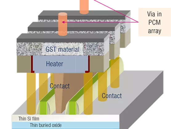
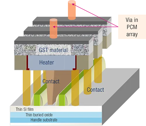
STMicroelectronics is now sampling 28nm FD-SOI microcontrollers (MCUs) with embedded non-volatile memory (eNVM) based on ePCM to alpha customers. Field trials meeting the requirements of automotive applications and full technology qualification are expected in 2020. These MCUs—the world’s first to use ePCM, which stands for embedded Phase-Change Memory—will target powertrain systems, advanced and secure gateways, safety/ADAS applications, and Vehicle Electrification. (Read the full press release here.) [caption id="attachment_14593" align="alignright" width="300"] A cross section of the embedded-PCM bitcell integrated in the 28nm FD-SOI technology shows the heater that quickly flips storage cells between crystalline and amorphous states. (Courtesy: STMicroelectronics)[/caption] “Having applied ST’s process, design, technology, and application expertise to ePCM, we’ve developed an innovative recipe that makes ST the very first to combine this non-volatile memory with 28nm FD-SOI for high-performance, low-power automotive microcontrollers,” said Marco Monti, President Automotive and Discrete Group, STMicroelectronics. “With samples already in some lead-customers’ hands, we’re confirming the outstanding temperature performance of ePCM and its ability to meet all automotive standards, further assuring our confidence in its market adoption and success.” ePCM presents a solution to chip- and system-level challenges, meeting automotive MCU requirements for AEC-Q100 Grade 0, operating at temperature up to +165°C. In addition, ST says its technology assures firmware/data retention through high-temperature soldering reflow processes and immunity to radiation, for additional data safety. Architecture and performance benchmark updates were presented the most recent IEDM (December 2018 in San Francisco) in a paper entitled Truly Innovative 28nm FDSOI Technology for Automotive Micro-Controller Applications embedding 16MB Phase Change Memory (F. Arnaud et al). As of this writing, the IEDM 2018 papers are not yet posted on the IEEE Xplore Digital Library site. However, the ppt that ST presented at the conference is available here. For more in-depth information on ePCM, see the ST PCM page. To learn more about how it compares with competing technologies such as eMRAM, read Embedded Phase-Change Memory Emerges by Mark Lapedus of SemiEngineering. Papers describing other eNVM solutions on FD-SOI were also presented at IEDM 2018. Samsung's is entitled Demonstration of Highly Manufacturable STT-MRAM Embedded in 28nm Logic (Y. J. Song et al). GlobalFoundries' is entitled 22-nm FD-SOI Embedded MRAM Technology for Low-Power Automotive-Grade-1 MCU Applications (K. Lee et al).
Read More
Five young dancers bathed in a striking rainbow of colors with their silhouettes cast in the background dazzled SEMICON Japan 2018 attendees at the opening ceremony in mid-December. Gone were the standard opening keynotes and ribbon cutting, replaced by live performance and media art set against a dramatic black backdrop. There was no mistaking the wide-eyed looks of wonder in the audience.In its sheer vibrance, the opening ceremony thrilled with an excitement that seemed to embody the extraordinary growth expectations for the global semiconductor supply chain over the next five years, with the industry poised to double sales from $2 trillion to a staggering $4 trillion – a phenomena SEMI president and CEO Ajit Manocha has called The Rebirth of the Semiconductor Industry. Driving this unprecedented growth will be SMART applications that are transforming industries and applications worldwide, powered by artificial intelligence (AI) and Internet of Things (IoT) technologies.The dramatic scene at SEMICON Japan 2018 was staged by Rhizomatiks, a media arts company that produced the Rio Olympic Games closing ceremony and is famous for its pop music spectacles. The company’s CTO, Motoi Ishibashi, the event’s first keynote speaker, described his team’s development of drones and vehicles guided by motion and precision-control technologies. It was some of these SMART vehicles that maneuvered the opening ceremony performers from the dance company Elevenplay onstage. Only Rhizomatiks, Ishibashi said, has this capability. In its mission to enrich people’s lives through new media arts, Rhizomatiks uses the latest virtual and mixed-reality technologies to orchestrate not only dance performances but music videos, commercials, fashion shows and festivals.Toru Nishikawa, the second keynote speaker and CEO at Preferred Networks, a leading Japan-based developer of deep learning software programs, surprised the SEMICON Japan audience with his discussion of his company’s work to develop a specialized chip for deep learning processing, joining technology giants Apple, Google, Alibaba and Microsoft in chip design. As more IT and software companies develop specialized, differentiated chips, the devices are quickly becoming the heartbeat of SMART technologies. The company’s approach has taken hold. Only four years old, Preferred Networks is enjoying rapid growth by working with global powerhouses including Toyota, NTT, Panasonic, Fanuc, NVIDIA, Intel and Microsoft. Ishibashi’s and Nishikawa’s fresh visions and the media arts extravaganza reflected the success of SEMICON Japan, held again at Tokyo Big Sight: The event’s 1,881 booths – filled by 727 exhibitors from 14 regions – was the highest count in six years. With Japan home to companies that supply about 40 percent of semiconductor equipment and materials worldwide, top suppliers historically have occupied the largest spaces on the SEMICON Japan show floor.According to IDC, personal computers and smartphones, long the largest revenue sources for the semiconductor industry, will remain top revenue drivers in the coming years. But revenue from new SMART technologies for applications such as automotive and factory automation is growing, a trend expected to continue with a 2018-2022 CAGR of 9.5 percent for automotive and 5.2 percent for manufacturing, compared to 1.1 percent for PCs and 2.9 percent for smartphones.SEMICON Japan’s new SMART Applications zone highlighted these and other new market opportunities for semiconductor growth with product and technology exhibits from companies including Bosch, IBM, Microsoft, NEC, Preferred Networks, Sony, SAS, Siemens, Tesla and Toyota. But the zone wasn’t all work and no play. The ROBOT SQUARE and SPORTS x IOT robot exhibits took visitors back to their school days, with robot anime – from Astro Boy to Gundam and Evangelion – that they could ride and control! As the World Gets Smarter, So Must SEMICON and the IndustryWe all agree the world is getting smarter at a fast pace. New cars are easier to drive – some models are almost fully autonomous on highways and streets. Your SMART speaker has gone well beyond an audio playback device and is more like a home AI platform. Almost all storefronts are equipped with video cameras. Your workplace, whether an office or a factory, is driven by automation. The reliance of these environments and devices on semiconductors is driving exponential chip and changing the world. Businesses need to adapt and so do SEMICON events. We’re doing just that as SEMICON Japan 2018 demonstrated – from an opening ceremony enabled by technology innovation to new faces of the industry to the SMART Application zone. As the SEMICON Japan presidents’ reception concluded the first day of the show, a robot from the ROBOT SQUARE suddenly appeared in the reception hall in front of about 250 executives from the global industry. Everyone at the reception was impressed and stepped forward to the stage, reflecting the overall excitement about SEMICON Japan, which for many years showcased only chip manufacturing equipment and materials. This year, to keep pace with the changing world, it was much more than that.SEMICON Japan 2019 will again take place in December at Tokyo Big Sight. However, organizers of the Tokyo Olympics will be using the East Exhibit Hall usually occupied by SEMICON Japan to prepare for the games. As a result, SEMICON Japan will be held in the West and South Halls instead. Look for more changes to the event. I hope to see you next year!Jim Hamajima is president of SEMI Japan.
Read More
SEMI spoke with Antoine Amade, Regional Senior Director EMEA at Entegris, about the challenges set by the car industry, and the concept of “zero defect” and the need for a collaborative approach ahead of his presentation at the Strategic Materials Conference at SEMICON Europa 2018, 13-16, November 2018, in Munich, Germany. To register for the event, click here.SEMI: The automotive industry is setting new challenges. This is very exciting source of growth for the global supply chain, but what are in your opinion the automotive requirements of the future?Amade: By 2030, 50% of the car cost will be electronics related. With the autonomous cars, there will be no tolerance for any type of chip defects because it will have a direct impact on human safety. With that in mind, higher reliability, increased efficiency and control across the supply chain will be the main requirements of the automotive industry.SEMI: Is the New Collaborative Approach the solution to overcome the challenges related to the automotive requirements of the future such as defects and contamination? What can you tell us about this approach?Amade: The automotive industry presents a great challenge to all of us, reaching the ppb level in terms of defectivity. In other words, this zero defects objective requires a collective awareness and understanding: Within an aging and more complex manufacturing environment, we all need to challenge the status quo and go for a new collaborative approach.SEMI: What does Entegris propose?Amade: We trust that contamination control has a major role to play to reach the zero defects. We are now in the 3rd generation of contamination control. After the focus on the cleanroom environment and equipment, materials are now at the center of the attention. With Entegris offering the broadest portfolio in terms of advanced chemicals, filtration and purification, and materials handling, we’re uniquely positioned to address precision, purity, integrity, and safety challenges.SEMI: How could this support fab managers in their daily challenges and mid-term future objectives?Amade: The new collaborative approach is a journey. It is a consultative process to provide a fresh set of eyes and expertise on the key areas of concerns in the fabs. It is a multidisciplinary approach with zero defectivity as the main goal. It is focused on base line improvement, better process control, more uniformity and prevention of excursions.SEMI: What do you expect from SEMICON Europa Strategic Materials Conference?Amade: It's the perfect platform to deliver our message in front of the whole ecosystem. It obviously concerns the fabs, but also material suppliers, and even carmakers. We expect this new view of collaboration will create an engagement from all parties. It is not a coincidence that this is called New Collaborative Approach. Antoine Amade joined Entegris in 1995 as an application engineer in its semiconductor business. In his current role as EMEA Sr. Regional Director, Mr. Amade manages a sales, customer service and marketing team responsible for growing the semiconductor business in Europe and Middle East.Mr. Amade held leadership positions at Entegris including gas microcontamination market management, strategical account management and regional sales management. He has a degree in Chemical Engineering from ENS Chimie Lille and is a member of Semi Electronic Materials Group for Europe. Serena Brischetto is a marketing and communications manager at SEMI Europe.
Read More
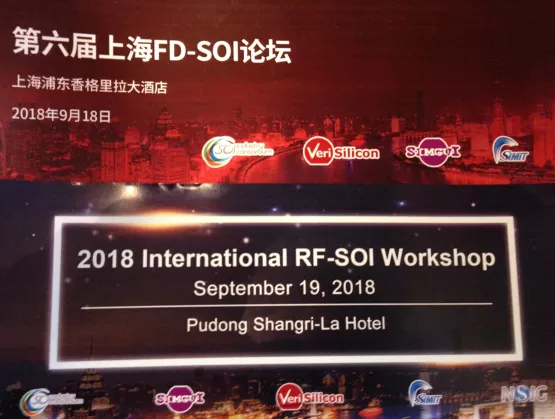
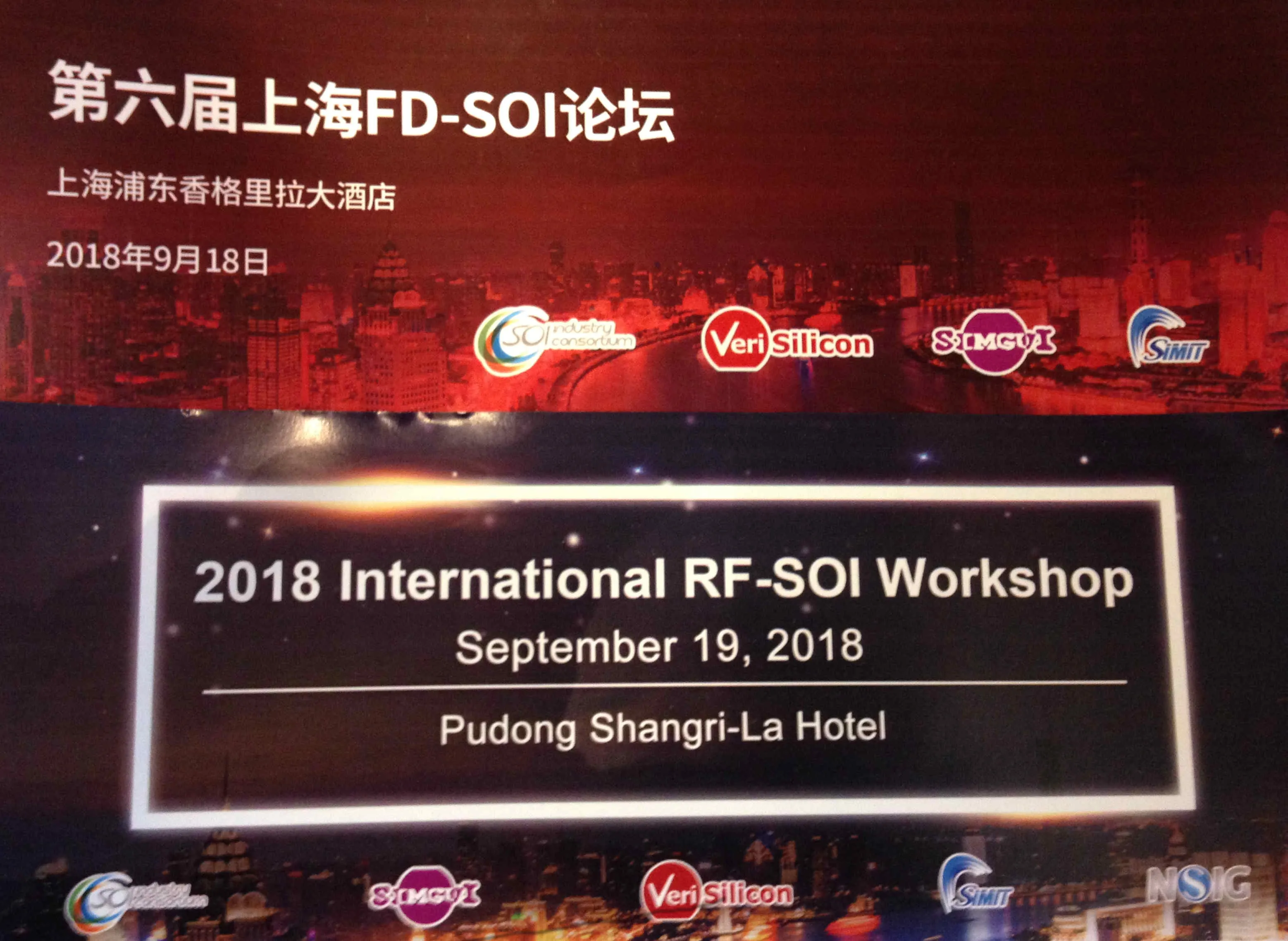
Excellent news and exciting applications made headlines at the recent FD-SOI and RF-SOI events in Shanghai. During the FD-SOI day, Amazon/Blink and Intellifusion shared news about their new chips, and we got updates from GF and Samsung. The RF-SOI day featured a great talk with details about China Mobile's 5G plans, and peeks at Nokia's groundbreaking approach and Qorvo's outlook. [caption id="attachment_12354" align="alignright" width="300"] (Photo courtesy: Verisilicon)[/caption] The hall was absolutely full – with over 300 people attending each day. The FD-SOI event was by invitation only, and there were far more people wanting to attend than there was room for, even given the big room in which the events were held. The events got excellent coverage in the China tech press. For example, EEWorld started with an overview article and added five supporting pieces zooming in on key presentations and companies: one on GlobalFoundries, one on Samsung, one on Verisilicon, and two on Soitec (CEO and top exec interviews). These pieces are in Chinese, but just open the links through your favorite translation site. Many of the key slides are captured in these articles, so if you can't wait for the ppts to be posted on the SOI Consortium website, you can get some quick previews now. The Verisilicon PR folks also wrote up highlights of the FD-SOI event in real time with lots of great pictures – you can read that here. Many thanks to that team, too, for flagging the coverage in the China press and posting it on their WeChat account. On the RF-SOI side, the Simgui folks wrote that up – you can read it here. They also sponsored a gala dinner with awards given to Qorvo and SmarterMicro – you can read about that here. Most of the presentations will be posted on the SOI Consortium website over the next few weeks, at which point we'll cover them in-depth here at ASN. But for now, here's a quick round-up of some of the highlights. FD-SOI Highlights [caption id="attachment_12347" align="alignright" width="300"] (Courtesy: Blink, Verisilicon)[/caption] Boston-area based Blink, which makes very popular home security systems, was recently bought by Amazon (see their current product page here). They just taped out a new chip on Samsung's 28FDS FD-SOI technology, and they're really happy about it. “I believe for battery powered devices at home, FD-SOI is the way to go,” said Yantoa Jia, Head of ASIC China Ops at Blink. Their goal in the move from 55nm bulk to 28nm FD-SOI was to double battery life, add features and control costs: and they did it. Even adding two more CPU cores and lots more features, “The power drop is fantastic,” he said. Design was no problem, he continued, and there was plenty of IP. Once the new generation is officially announced, he promised to sit down with ASN and give us more details. Attendees also heard about a new chipset from Intellifusion, which is putting its face recognition technology onto GlobalFoundries' 22FDX FD-SOI with design house Verisilicon. CEO Nin Chen gave an impromptu talk about how their technology is used to find missing people and property. The new chip, which is especially designed for use in cities, is network-to-cloud leveraging AI. For his part Thomas Morgenstern, GlobalFoundries SVP and GM of the Dresden Fab 1, said they're seeing high yields and increasing capacity for 22FDX. The marketing and manufacturing ecosystem has been built around the fab in Europe. Now, he said, the key is to build an FD-SOI ecosystem in China. The market needs of China largely parallel those of Europe, he noted, for performance and efficiency at the right cost point. The ecosystem enables fast time-to-market and 1st-time-right. [caption id="attachment_12343" align="alignleft" width="300"] (Photo courtesy: Cadence)[/caption] Samsung SVP Gitae Jeong sees their FD-SOI technology as the right solution for the 4th Revolution, which includes everything from energy harvesting to self-driving cars. They've just taped out their first 5G mmWave cellular chip on 28FDS, he revealed. eMRAM is looking very good, only requiring three additional masks and getting stable yields from -40o to 105oC. 18FDS is on schedule, with PDK 0.5 now being released, and 1.0 on track for release in March 2019. They expect a very fast ramp, and are looking at a 35% area reduction, power cut in half and performance up 22% compared to 28FDS. RF-SOI Highlights [caption id="attachment_12350" align="alignright" width="300"] China Mobile, Project Manager Danni Song (Photo courtesy: Simgui)[/caption] When China Mobile talks, the world listens. Project Manager Danni Song presented again this year (she gave a great talk last year, too). China has a very ambitious 5G project underway, and under two years in which to roll it out. The biggest challenges are power consumption and cost (a problem made worse by the additional power amplifiers needed for MIMO). Can RF-SOI help solve these challenges, she asked? One thing she did clarify during the panel discussion was with respect to the mmWave part of the 5G puzzle. Their initial 2020 rollout will only focus on sub-6GHz, with mmWave following a year or two later. Michael Reiha, Head of RFIC R D at Nokia Mobile Networks clarified the worldwide 5G rollout during the panel discussion. Different locations on the planet have different histories and needs, so will rollout 5G in different ways. For historical reasons (and a lack of choice), the US will lead with mmWave, he said. Europe, meanwhile, will focus on 24GHz to meet the needs of automotive radar. In his presentation, Reiha described Nokia's approach to power amplifiers (PA), which is very different from what others are doing. With RF-SOI, he said, you can add sensors and logic for a level of preventative care, so you can gauge and protect your equipment using AI. He believes this disruptive approach will put them two years ahead of the industry, enabling massive MIMO to be deployed in dense urban areas with 60% lower power consumption and 50% savings in material costs. Go read about their Reefshark tech, he urged, which he says will beat GaAs. “The future is very bright with RF-SOI,” he concluded. “I can state that with confidence.” [caption id="attachment_12351" align="alignleft" width="300"] Julio Costa, Director of Technology Development, Qorvo (Photo courtesy: Simgui)[/caption] Julio Costa, Director of Technology Development at Qorvo sees it differently. Traditionally a GaAs house, all their RF-SOI work is fabless. While RF front end modules (FEMs) are loaded with RF-SOI, he said, and are a big winner for antenna tuning, Qorvo still sees GaAs for high-efficiency amplifiers and envelope tracking. But, he said, it will be a battle. GaAs wins in terms of area and power consumption he contends, but adds that SOI wins in terms of cost. Power levels, he predicts, will be the determining factor. So that's the quick overview – we'll drill down into the presentations as they're posted, so stay tuned!
Read More
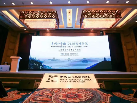
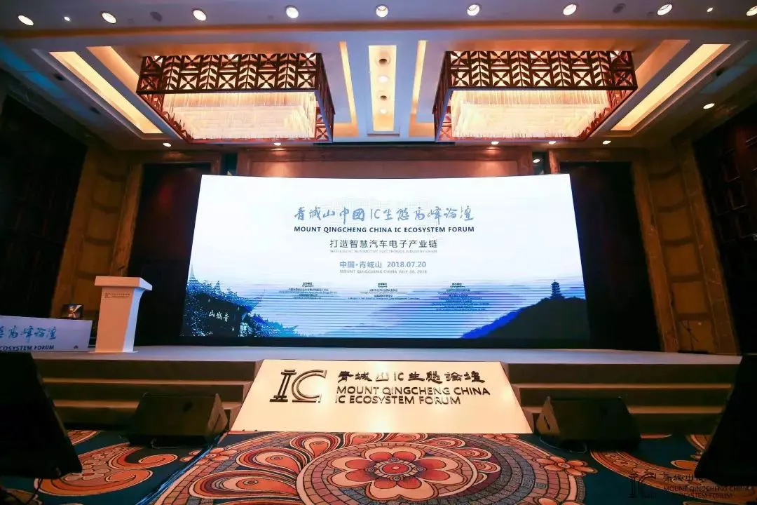
FD-SOI was a very important topic during the recent Mount Qingcheng China IC Ecosystem Forum. To situate things, Mount Qingcheng, with its lush hills and waterways, is located just outside of Chengdu. That of course is where GlobalFoundries is building its new fab, which will be the first in China to run FD-SOI. Chengdu is also a key city in China's automotive electronics landscape. [caption id="attachment_12236" align="alignright" width="300"] (Image Courtesy: VeriSilicon)[/caption] The theme of the forum was Building a Smart Automotive Electronics Industry Chain. Over 260 decision-makers from government, academia and industry attended – and the SOI Consortium had a significant presence. The event was chaired by Wayne Dai, CEO/Founder of consortium member VeriSilicon, and tireless champion of the the FD-SOI ecosystem in China and worldwide. Morning keynotes were given by: Carlos Mazure, Soitec CTO and SOI Consortium Executive Co-Director; Mark Granger, GF's VP of Automotive Product Line Management; and Tony King-Smith, Executive Advisor at AImotive, a GF 22FDX customer. BTW, transcripts of all the talks are available through Gasgoo, China's largest automotive B2B marketplace. You can click here to access them. (They're in Chinese – but you can open them in the language of your choice using the major translation websites.) Chengdu Officials Affirm Support for FD-SOI Fan Yi, Deputy Mayor of Chengdu, spoke extensively of FD-SOI in his keynote on the importance of rapidly developing smart cars. He heralded the “spectacular” new GlobalFoundries fab there. Following a meeting with the company's top brass the day before, he affirmed GF's confidence in their investment. There is a solid roadmap for FD-SOI, he noted, and efforts are underway to accelerate the move into production and expand education and training. He cited the benefits of FD-SOI for the entire supply chain, from design through package and test, raising the level of the entire IC industry to new heights. The government, he said, attaches great importance to this enterprise. Their thinking regarding intelligent transport in China is integrated with the overall approach to smart cities. SOI Consortium Leads Industry Keynotes [caption id="attachment_12232" align="alignleft" width="300"] Wayne Dai, VeriSilicon Founder and CEO (Photo courtesy VeriSilicon)[/caption] In his opening remarks, Wayne Dai emphasized the need for China to seize the advantage in the next round of development opportunities in the automotive electronics industry. This year's Qingcheng forum, he noted, brought together key representatives from across the supply chain, from of the highest to the deepest reaches of the smart car electronics industry, and across markets, technologies, solutions, industrial ecosystem, standards and regulations. In his talk on how FD-SOI is boosting the accelerated development of automotive electronics, Carlos Mazure presented the SOI Industry Consortium. He noted that the Consortium promotes mutual understanding and development across the ecosystem. SOI is already present throughout automotive applications, he noted. There are currently about 100mm2 of SOI per car, in such diverse areas power systems, transmissions, entertainment, in-vehicle networking and more. SOI will experience especially high growth in electrification, information/entertainment, networking, 5G, AI/edge computing and ADAS. He then went on to give some history and an extensive overview of the major trends and highlights we've seen over recent years. He finished by giving examples of convergence across the supply chain with IC manufacturers working with automakers to lower power, increase processor performance and advance 5G. [caption id="attachment_12233" align="alignright" width="665"] Carlos Mazure, Soitec CTO and SOI Consortium Executive Co-Director; Tony King-Smith, Executive Advisor at AImotive and Mark Granger, GF's VP of Automotive Product Line Management (Photo courtesy VeriSilicon)[/caption] GF's Mark Granger addressed the rapid development of automotive electronics. In certain areas, he said, he sees growth rates of over 20%. They are working on building the Chengdu ecosystem, especially for design, and in cooperation with the rest of the supply chain. Furthermore, he reminded the audience, when you talk about cars, travel implies that you also talk about IoT as well as things like infotainment and integrated radar ICs. In addition to cost and power efficiencies, the AEC-Q100 standard for IC reliability in automotive applications is also pushing designers to turn to FD-SOI. In the GF meeting with Chengdu government officials (referenced above in deputy mayor Fan Yi's talk), he too confirmed their support of FD-SOI as a key technology for China. GF is currently cooperating with about 75 automotive partners, he said, and the company is looking to increase cooperation with partners in the Chengdu region. Tony King-Smith talked about the 22FDX test chip AImotive is doing with Verisilicon and GF. In case you missed it, in June 2017 AImotive announced its AI-optimized hardware IP was available to global chip manufacturers for license. AiWare is built from the ground up for running neural networks, and the company says it is up to 20 times more power efficient than other leading AI acceleration hardware solutions on the market. In the same announcement, they revealed that VeriSilicon would be the first to integrate aiWare into a chip design,and that aiWare-based test chips would be fabricated on GF's 22FDX. The chip is expected to debut this year. While the afternoon agenda was not specific to FD-SOI, it did focus on the "smart cockpit" and "intelligent driving", with talks by nine leading players in China's automotive IC and investment communities. ~ ~ ~Note: Many thanks to the folks at VeriSilicon, who wrote up this event for their WeChat feed, and shared photos with us here at ASN.
Read More
The Japan semiconductor manufacturing supply chain is a global semiconductor industry workhorse, producing about one third of world’s chip equipment and more than half of its semiconductor materials. In contributing the vast majority of these products, SEMI Japan member companies hold the high distinction of enabling continuous development of the worldwide semiconductor industry. Aptly, then, technology powerhouses IBM, Nissan Motors and Toshiba offered insights into the latest trends and innovations in computing and smart cars at the late-May SEMI Japan Members Days in Tokyo with 133 technologists from member companies in attendance. As the audience discovered, chip innovation never sleeps and, as futuristic as it can be, invariably gives rise to possibilities beyond the human imagination. That was the message of kickoff presentation “Computing Reimagined – AI/Quantum/IoT” – by Dr. Shintaro Yamamichi, Senior Manager, Science Technology at IBM Research-Tokyo. Dr. Yamamichi cited three examples of how semiconductors uncover new technology frontiers. Computational materials discovery, a novel methodology, is the application of theory and computation to unearthing new materials and the key to enabling an ongoing stream of semiconductor innovation. In particular, using cognitive technology to mine huge volumes of literature reveal new insights into materials that uncover even more functionality such as greater conductivity and heat resistance. With new materials the oxygen of ever more advanced semiconductor chip manufacturing, the semiconductor industry will surely benefit from this methodology. The opportunity to accelerate quantum computing innovation is now. Launched in May 2016, the IBM Quantum Experience gives students, researchers and general science enthusiasts hands-on access to IBM’s experimental cloud-enabled quantum computing platform. The online platform features a forum for discussing quantum computing topics, tutorials on how to program IBM Q devices, and other educational material about quantum computing. Dr. Yamamichi encouraged the audience to join the program. The world’s tiniest computer, unveiled by IBM at the company’s Think 2018 conference in Las Vegas, packs several hundred thousand transistors and, IBM claims, the equivalent power of a 1990s x86 chip into a package smaller than a grain of salt. The computer’s small form factor (less than 1mm x 1mm) and low manufacturing cost means it can be embedded in product price tags and packages as an anti-fraud device using blockchain technology. Vehicles need to be both electric and intelligent as countries become more populous and traffic density increases. More drivers extend average drive time, boost greenhouse emissions, devour precious energy resources and lead to more traffic congestion and accidents. Dr. Haruyoshi Kumura, fellow at Nissan Motor, highlighted these issues in stressing the importance of a new era of intelligent mobility. To mitigate these problems, Nissan is focusing on the electrification and intelligence of its vehicles: Nissan’s electric vehicle, Leaf, reduces accidents with electric intelligence systems such as e-Pedal, which uses an accelerator pedal only for both acceleration and deceleration, and ProPILOT Park, a feature that automatically parks the car by using multiple cameras and ultrasonic sonars to detect pedestrians and other objects around the vehicle. With more than 90 percent of traffic accidents caused by driver error, Nissan plans to introduce autonomous driving on multi-lane highways by the end of 2018 and on city streets by 2020. By 2022, the company plans to roll out full autonomous driving to reduce traffic accidents caused by inattentive drivers. For full autonomous driving to materialize, sensor fusion technology must incorporate a combination of technologies – radar systems, light detection and ranging (LiDAR) systems and cameras – to identify the shapes and locations of nearby moving objects and measure their speed. Sensed information is then processed by a 3D graphic analyzer to make electric throttle, braking and steering decisions. The outlook for automotive industry includes car sharing and more electrification – both insights from Yoshiki Hayakashi, general manager, automotive solution strategic planning division at Toshiba Electronic Devices Storage, who offered his perspectives on trends in Japan’s automotive industry and beyond. To meet the requirements of the COP21 Paris agreement, the global automotive industry is shifting to electrification. Toshiba estimates 60 percent of new cars will be electric vehicles by 2040 to meet the International Energy Agency’s global EV outlook. In Japan, autonomous driving or advanced driver assistance systems (ADAS) will be offered in certain areas by 2020, the year of the Tokyo Olympic games. Growth of these advanced driving systems hinges on infrastructure development. Supporting data centers, intelligent transport systems, vehicle-to-everything connections, and smart city are all necessary components. Car ownership will begin to cede ground to car sharing with technology elites such as Tesla, Apple and Google leading the way. To expand the car-sharing industry, new alliances will take shape between new and old-guard automotive companies and electronics manufacturing services (EMS) providers. Autonomous driving requires precise 3D renderings of actual roadways using sensors for route mapping. While sensor fusion must be deployed for these capabilities, LiDAR offers better sensing range and space resolution precision than ultrasonic sonars, radars, and cameras. The next SEMI Japan members day is scheduled for October 30 in Tokyo. SEMI holds similar events in most regions where SEMI and its members operate. For the members events in your region, contact the SEMI office nearest you. Yoichiro Ando is a marketing director in SEMI Japan.
Read More
Dolphin Integration, a partner in the ENIAC THINGS2DO European FD-SOI project, showcased its achievements with PowerStudio™ during the project final review. Power Studio is Dolphin's cutting-edge EDA tool for safe Power Regulation Networks implementation. THINGS2DO, which stands for THIN but Great Silicon to Design Objects, was a 4-year, €120 million EU project (85% industry-funded) with over 40 partners that just finished up at the end of 2017. The goal was to build a design development ecosystem for FD-SOI. The project funded and supported the development of major FD SOI-based IPs and ASICs as well as EDA tools. (Another recent THINGS2DO announcement was Dream Chips’ ADAS SoC fabbed in GlobalFoundries’ 22FDX technology -- read about that here.) “Being involved in the THINGS2DO project was an opportunity for Dolphin Integration to start introducing FD-SOI in its automatic design methodologies,” said Frederic Poullet, Dolphin Integration’s CTO (read the press release here). “Dolphin Integration plans to offer a full suite of tools allowing its customers to implement right-on-first-pass Power Regulation Networks.” The company notes that THINGS2DO also proved that low power consumption makes FD-SOI a perfect fit for IoT and automotive applications. For instance, dynamic control of threshold voltage can be used to compensate for temperature variations, and to drive speed improvements by 200% in ultra-low voltage applications. Dolphin Integration provides energy efficient IPs and ASIC services dedicated to the low-power application market and supports its internal teams with tailor-made software tools. To address the specific needs of its customers in low-power design, Dolphin developed PowerStudio™, a global solution for the optimization of Power Regulation Networks (PRNet) to be used at an early stage of the SoC design process. In particular, it addresses new design challenges in noise and power supply integrity. The first module of PowerStudio™ will also embed architecture optimization features at the schematic level, in terms of FoM-based cost optimization, mode management, margin cuts and integrability rate-based risk optimization. Btw, Dolphin Integration Director Frederic Renoux gave an excellent great presentation at an SOI Consortium event in Nanjing, China last year, entitled Embedding power regulation activity control networks for best SoC PPA. Dolphin Integration joined Global foundries’ FDXcelerator™ Program last year (read the press release here) to streamline design in 22FDX®. "Our comprehensive and robust library of voltage regulators, power gating cells and logic modules, enables to deal cost-effectively and securely with power distribution, power gating, power monitoring and power control of any SoC design in 22FDX," Michel Depeyrot, Dolphin Integration's Chairman, said at the time. "As connected devices sleep most of their time, users of 22FDX also benefit from our ultra-low power and accurate oscillators to design an always-on RTC which consumes as little as 60 nA." See the Dolphin Integration website for the full catalog of their IP, EDA and ASIC/SoC service offerings, including for GF's 22FDX.
Read More
What’s next for smarter, more connected electronics manufacturing - Part 1The fast-maturing infrastructure now enabling applications for big data and artificial intelligence means disruptive change not just at individual companies but also in data connections among companies across the microelectronics manufacturing value chain. SEMI expands its smart manufacturing program with a Smart Manufacturing Pavilion with displays and three full days of talks to address these industry-wide developments at SEMICON West, July 10-12 in San Francisco.Autonomous autos’ demand for zero-defect systems and 100 percent traceability back to the manufacturing data for each die is driving a push to traceability across the chip sector. “Far more chips are being used by the automotive sector, and its very different requirements are driving demand for traceability,” says Tom Ho, president of BISTel America. “Our chipmaker customers are looking for traceability solutions and the trend is the same in backend packaging and assembly – automotive applications are driving the sector to traceability.”Traceability is also driven by the growth of systems in a package as fabless chipmakers look to connect back to the packaging companies’ fault analysis labs and die interconnect history to diagnose and fix the cases where known-good die are failing in the system, adds Mike Plisinski, CEO of Rudolph Technologies. Plisinski adds that makers of consumer products like phones that can also see harsh conditions are demanding higher quality and traceability as well. The electronic manufacturing services (EMS) sector also must establish an architecture for traceability to collect critical manufacturing-related data and to interface with OSATs and semiconductor fabs. The reason is that EMS companies are adding traditional OSAT processes such as assembly of products with bare die and complex optics modules requiring clean rooms. “A unified sand-to-smart-phone smart manufacturing roadmap should be established,” says Dan Gamota, vice president of Engineering and Technology Services at Jabil. “We need to identify protocols for manufacturing data communications that can be adopted across the supply chain.”To enable smart manufacturing, vendors need to collaborate on getting their production equipment to interoperate and support factory analytics and data management systems. Source: SEMI One big challenge, of course, is how to format this diverse data so it can be linked and used by various supply chain stakeholders. “Smart data needs to be contextual and it needs data standards across the supply chain so it’s easy to link from the front end to the back end, follow common lot IDs front and back end, and have a way to map streaming data from sensors to a discrete lot ID,” notes Ho. New approaches to metrology, analysis and test that increasingly exploit machine learning on simulations will also be needed to help predict which die and connections that test well now may fail in the future as conditions change.Another issue is how to securely share the needed data across companies without jeopardizing IP. “On the equipment side we collect data across customers on how the tool is running to improve the equipment,” notes Neal Callan, ASML VP Silicon Valley. “Next we need to integrate performance and reliability data that today is not as well shared.”The other big hurdle is how to pay for data sharing. “The challenge is that the final manufacturers reap the benefit of traceability, but since they expect their suppliers to deliver good die, they don’t want to pay more for it,” notes Plisinski. He suggests that over the next two to three years, traceability and predictive fault prevention will become the norm as the automotive sector is compelled to invest in it to assure safety. Meanwhile, fabless companies will face so much complexity in integrating different die from different suppliers in SiP that they will no longer be able to afford to simply use the cheapest supplier, potentially driving a fundamental shift in relations and division of labor among fabless chipmakers, OSATs and fabs. Standards extend across supply chainSEMI member committees are collaborating to build the infrastructure to enable these developments. Standards committees are updating standards for higher bandwidth data exchange and extending semiconductor-like vertical and two-way horizontal equipment communication standards to flow shops to enable assembly players to optimize and trace back results across players. The SMT/PCBA community is integrating its smart manufacturing work into SEMI standards, and the SEMI A1 standard was a key reference document in the development of the Japan Robotics Association’s Equipment Link Protocol.Speakers addressing these issues at SEMICON West include Active Layer Parametrics, Applied Materials, Applied Research Photonics, ASML, Bosch Rexroth, Cimetrix, Coventor, ECI Technologies, Edwards Vacuum, Final Phase Systems, GE Digital, Infineon, Jabil, Lam Research, Osaro, Otosense, PEER Group, Qualcomm, Rockwell Automation, Rudolph Technologies, Schneider Electric, Seagate, Siemens, Stanford University, TEL, TIBCO Software. See semiconwest.org.What’s next for smarter, more connected electronics manufacturing - Part 2What’s next for smarter, more connected electronics manufacturing - Part 3Paula Doe, SEMI
Read More