downloadGroupGroupnoun_press release_995423_000000 copyGroupnoun_Feed_96767_000000Group 19noun_pictures_1817522_000000Member company iconResource item iconStore item iconGroup 19Group 19noun_Photo_2085192_000000 Copynoun_presentation_2096081_000000Group 19Group Copy 7noun_webinar_692730_000000Path
Skip to main content
Default Banner Image

Semiconductor Fabs

The China IC Ecosystem Report, a comprehensive report for the IC manufacturing supply chain, reveals that front-end fab capacity in China will grow to account for 16 percent of the world's semiconductor fab capacity this year, a share that will increase to 20 percent by the end of 2020. With the rapid growth, China will top the rest of the world in fab investment in 2020 with more than $20 billion in spending, driven by memory and foundry projects funded by both multinational and domestic companies, according to the new report released today by SEMI.The report also shows that IC Design remained the largest semiconductor sector in China for the second year in a row with $31.9 billion in revenue in 2017, widening its lead over the long-dominant IC Packaging and Test sector. The ascent of China’s IC Design sector comes as the region’s equipment market is expected to claim the top spot in 2020 for the first time on the strength of the continuing development of its domestic manufacturing capability. China’s maturing domestic fab sector is also benefiting domestic equipment and materials suppliers. Both groups continue to see gains in their product offerings and capabilities, particularly in silicon wafer production. The China IC Ecosystem Report is produced by SEMI, the global industry association and provider of independent electronics market research.The more than RMB140 billion (US$21.5 billion) accumulated by the National IC Fund, a critical component of the 2014 National Guideline to address China’s semiconductor trade deficit, has spurred rapid gains throughout the region’s IC supply chain. Semiconductors are China’s largest import by revenue. Phase 2 of funding aims to raise another RMB150-200 billion ($23.0-$30.0 billion).Encouraged by the National Guideline and favorable policies, skilled overseas talent is returning to China, triggering an explosion of domestic IC Design start-ups that are benefiting from access to investment and favorable policies, the report shows.Other highlights from The China IC Ecosystem Report include: Currently 25 new fab construction projects are underway or planned in China. 17 - 300 mm fabs are being tracked as part of this investment and expansion activity. Foundry, DRAM and 3D NAND are the leading segments for fab investment and new capacity in China. China’s IC Packaging and Test industry is also moving up the value chain by enhancing its technology offerings through mergers and acquisitions and building advanced capabilities to entice international integrated device manufacturers. China’s IC materials market, currently dominated by Packaging materials, became the second largest regional market for materials in 2016, a position it solidified in 2017. China’s materials market is expected to grow at a 10 percent CAGR from 2015 to 2019, driven primarily by the region’s new fab capacity ramp in the coming years. Fab capacity will expand at a 14 percent CAGR during that period. The China IC Ecosystem Report covers the latest semiconductor supply chain and market developments including the rise of China’s IC industry, national and local government policies, public and private funding, and their implications for China's IC supply chain. The report also compares key domestic companies and their international peers segment by segment. To learn more and get a sample of the report, visit http://www.semi.org/en/china-ic-ecosystem-report.Eugenia is a Senior Product Marketing Manager at SEMI.
Read More
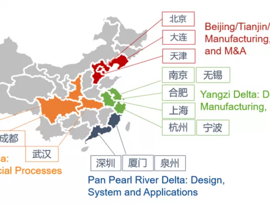
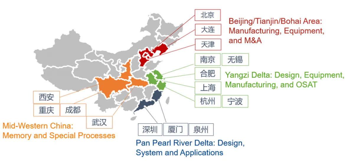
What’s next for smarter, more connected electronics manufacturing - Part 1The fast-maturing infrastructure now enabling applications for big data and artificial intelligence means disruptive change not just at individual companies but also in data connections among companies across the microelectronics manufacturing value chain. SEMI expands its smart manufacturing program with a Smart Manufacturing Pavilion with displays and three full days of talks to address these industry-wide developments at SEMICON West, July 10-12 in San Francisco.Autonomous autos’ demand for zero-defect systems and 100 percent traceability back to the manufacturing data for each die is driving a push to traceability across the chip sector. “Far more chips are being used by the automotive sector, and its very different requirements are driving demand for traceability,” says Tom Ho, president of BISTel America. “Our chipmaker customers are looking for traceability solutions and the trend is the same in backend packaging and assembly – automotive applications are driving the sector to traceability.”Traceability is also driven by the growth of systems in a package as fabless chipmakers look to connect back to the packaging companies’ fault analysis labs and die interconnect history to diagnose and fix the cases where known-good die are failing in the system, adds Mike Plisinski, CEO of Rudolph Technologies. Plisinski adds that makers of consumer products like phones that can also see harsh conditions are demanding higher quality and traceability as well. The electronic manufacturing services (EMS) sector also must establish an architecture for traceability to collect critical manufacturing-related data and to interface with OSATs and semiconductor fabs. The reason is that EMS companies are adding traditional OSAT processes such as assembly of products with bare die and complex optics modules requiring clean rooms. “A unified sand-to-smart-phone smart manufacturing roadmap should be established,” says Dan Gamota, vice president of Engineering and Technology Services at Jabil. “We need to identify protocols for manufacturing data communications that can be adopted across the supply chain.”To enable smart manufacturing, vendors need to collaborate on getting their production equipment to interoperate and support factory analytics and data management systems. Source: SEMI One big challenge, of course, is how to format this diverse data so it can be linked and used by various supply chain stakeholders. “Smart data needs to be contextual and it needs data standards across the supply chain so it’s easy to link from the front end to the back end, follow common lot IDs front and back end, and have a way to map streaming data from sensors to a discrete lot ID,” notes Ho. New approaches to metrology, analysis and test that increasingly exploit machine learning on simulations will also be needed to help predict which die and connections that test well now may fail in the future as conditions change.Another issue is how to securely share the needed data across companies without jeopardizing IP. “On the equipment side we collect data across customers on how the tool is running to improve the equipment,” notes Neal Callan, ASML VP Silicon Valley. “Next we need to integrate performance and reliability data that today is not as well shared.”The other big hurdle is how to pay for data sharing. “The challenge is that the final manufacturers reap the benefit of traceability, but since they expect their suppliers to deliver good die, they don’t want to pay more for it,” notes Plisinski. He suggests that over the next two to three years, traceability and predictive fault prevention will become the norm as the automotive sector is compelled to invest in it to assure safety. Meanwhile, fabless companies will face so much complexity in integrating different die from different suppliers in SiP that they will no longer be able to afford to simply use the cheapest supplier, potentially driving a fundamental shift in relations and division of labor among fabless chipmakers, OSATs and fabs. Standards extend across supply chainSEMI member committees are collaborating to build the infrastructure to enable these developments. Standards committees are updating standards for higher bandwidth data exchange and extending semiconductor-like vertical and two-way horizontal equipment communication standards to flow shops to enable assembly players to optimize and trace back results across players. The SMT/PCBA community is integrating its smart manufacturing work into SEMI standards, and the SEMI A1 standard was a key reference document in the development of the Japan Robotics Association’s Equipment Link Protocol.Speakers addressing these issues at SEMICON West include Active Layer Parametrics, Applied Materials, Applied Research Photonics, ASML, Bosch Rexroth, Cimetrix, Coventor, ECI Technologies, Edwards Vacuum, Final Phase Systems, GE Digital, Infineon, Jabil, Lam Research, Osaro, Otosense, PEER Group, Qualcomm, Rockwell Automation, Rudolph Technologies, Schneider Electric, Seagate, Siemens, Stanford University, TEL, TIBCO Software. See semiconwest.org.What’s next for smarter, more connected electronics manufacturing - Part 2What’s next for smarter, more connected electronics manufacturing - Part 3Paula Doe, SEMI
Read More
Can it be that no more new semiconductor fabs are being built in the U.S.?The last new volume fab known is Micron’s Building 60 in Utah, according to the SEMI World Fab Forecast report published in February 2018. The catch is Building 60 is not a new or greenfield facility but rather an existing structure being retooled for 3D NAND. Fab equipment spending for this fab is expected to be high in 2018.Then there is Fab 42 from Intel. Construction started in 2011 before it was shelved. It is expected to begin equipping by end of this year, with equipment spending expected to be high next year.Other fabs built many years ago are still ramping such as Globalfoundries Fab 8 phase 3 (TDC) and D1X (module 1 and module 2). D1X is a research and development pilot, not a high-volume fab. And Globalfoundries’ plans for a second fab in Malta have been pushed out.Samsung in Austin has space for more modules, but there is no indication they will ever be added.The SEMI World Fab Forecast shows five smaller facilities either planned or under construction, but these have little impact in this U.S. fab construction trend.And that’s basically it! No more volume fabs!If we divide fab equipment spending into two categories – investment in new capacity versus upgrades – we see a declining trend for fabs adding capacity. See chart below. (Compare 2005-2011 with 2017-2019). If we look at 2017, 2018 and 2019, Globalfoundries, Intel, and Micron are the big investors in new capacity.This year 60 percent of all fabs are expected to invest in equipment to add capacity, but just one or two volume fabs (Micron and Globalfoundries) account for the bulk of this growth. Same story for 2019, with two volume fabs (Intel and Globalfoundries) representing the lion’s share of the growth. Strike the Intel and Globalfoundries fabs from the equation, and investments in additional capacity would fall below upgrade spending levels.Once these fabs have reached full capacity, additional equipment investments will significantly lag spending increases for upgrades, signaling the end of new fabs in the U.S.
Read More
Large semiconductor fabs can devour electricity at clip of 100 megawatts per hour -- enough to power 50,000 homes1 and, according to a McKinsey study, more than automobile plants and oil refineries consume. So ravenous is their electricity consumption that some fabs have resorted to building their own captive power plants. Oversize fabs, depending on their location and local rates, can run up utility bills as high as $25 million each year, with electricity accounting for up to 30 percent of operating costs.Fabs use electricity to power HVAC, run cooling water, and for basic infrastructure. But the vast majority of electricity is gobbled up by semiconductor manufacturing process tools and their sub-fab support equipment such as vacuum pumps and abatement systems. In a typical fab, as much as 44 percent of the electricity is consumed by the processing equipment2. It’s not so hard to imagine. Etch and deposition tools need power to strike and sustain plasma, with multiple 1,000+ Watt RF power supply feeds per chamber and four, six or more chambers per tool, and vacuum pumps spinning and abatement running. The power load adds up quickly. Watts and WattsThe good news is that process tools aren’t processing wafers all the time. The bad news is that, in the past, there was no good way for the fab to know when process tools and support equipment weren’t running processes. Turning equipment off, or reducing power when not processing, wasn’t coordinated and standby states weren’t defined for readiness for a seamless power-up and return to processing. So what to do? Take action. That just what industry volunteers did when they met within SEMI’s Standards program and defined an equipment “idle mode” (SEMI E167 and SEMI S233). More recently, a SEMI Standard (SEMI E1754) was developed to define energy saving modes – how process tools communicate with sub-fab equipment, to reduce utility consumption when wafers are not being processed by the tool. Importantly, it also provides guidance on the standby state to return to full performance when the tool is needed to process wafers.5Good to be IdleThe semiconductor industry is now increasingly adopting a “smart idle” approach using these SEMI Standards. Fabs implementing these standards to take advantage of process tool idle periods can save more than 4.3 million € annually, according to AIS Automation modeling.6 This study also points to a savings of more than 16,000 tons of CO2 per year, the equivalent of taking more than 10,000 cars off the road.Who knew that recognizing when to be idle could bring such big rewards? If only I could apply that to my own life, but, for now, I will have to leave it to the fabs. SEMI International Standards volunteers make a huge difference to our industry every day. If you want to join the over 5,000 SEMI Standards volunteers (or join SEMI’s Sustainable Manufacturing eForum), with representation from over 2,000 companies, it’s free! Don’t be idle for this one, click here to join! http://www.semi.org/en/standards/P041367 1Bringing Energy Efficiency to the Fab, McKinsey 20132http://semiengineering.com/saving-energy-in-the-fab/3SEMI E167-1213 - Specification for Equipment Energy Saving Mode Communications (EESM)http://ams.semi.org/ebusiness/standards/SEMIStandardDetail.aspx?ProductID=211 DownloadID=32573SEMI S23-0813 - Guide for Conservation of Energy, Utilities and Materials Used by Semiconductor Manufacturing Equipmenthttp://ams.semi.org/ebusiness/standards/SEMIStandardDetail.aspx?ProductID=211 DownloadID=31094SEMI E175-1116 - Specification for Subsystem Energy Saving Mode Communication (SESMC)http://ams.semi.org/ebusiness/standards/SEMIStandardDetail.aspx?ProductID=211 DownloadID=38765http://electroiq.com/blog/2017/06/how-semi-standard-e175-is-saving-energ...6SEMI Standards a Potential Help for Saving Energy, Bert Mueller, AIS Automation 2016
Read More