downloadGroupGroupnoun_press release_995423_000000 copyGroupnoun_Feed_96767_000000Group 19noun_pictures_1817522_000000Member company iconResource item iconStore item iconGroup 19Group 19noun_Photo_2085192_000000 Copynoun_presentation_2096081_000000Group 19Group Copy 7noun_webinar_692730_000000Path
Skip to main content
Default Banner Image

Semiconductor Fabs

In my role as lead for the Smart Mobility initiative at SEMI, I recently spoke with Automotive Logistics Magazine about the growing importance of the semiconductor supply chain’s connection with the automotive industry and the semiconductor shortage hampering global automotive production. Following are excerpts from the interview. Automotive Logistics: Why is there a bottleneck in the global supply of semiconductors at the moment and how long is it likely to last? Weiss: The current automotive chip shortage resulted from the sharp, Covid-19-induced decrease in demand for automotive semiconductors in the second quarter of last year when vehicle production came to a near standstill. The automotive market picked up significantly in the fourth quarter and this caused the supply chain constraints we are seeing today. At the same time as the automotive standstill, the pandemic spurred an increase in demand for home computing and networking equipment, and semiconductor manufacturing plants (fabs) had to pivot to these other markets in order to maximize fab utilization and successfully navigate economic headwinds. Every minute a semiconductor fab is idle or has lines down adds up quickly to missed revenue, so their capacity is booked weeks and even months in advance. With this background, I don’t believe this is a structural shortage and expect a gradual recovery over the next two quarters, barring any major shifts in geopolitics or macroeconomics. Automotive Logistics: What needs to be done to remedy the current shortfall for the automotive industry? Weiss: The automotive industry needs to continue to strengthen its connections to the semiconductor manufacturing supply chain. In past years, auto manufacturers used to rely mainly on their tier one suppliers to interface with the semiconductor supply chain. This has changed significantly. Not only are more chips being used in vehicles (roughly 10% of all devices produced globally end up in cars), but the strategic importance of the chips as enablers for ADAS [advanced driver-assistance systems], electrification, safety, connectivity and other consumer-driven features has increased considerably. With this dynamic in play, carmakers have recognized the value of interacting and collaborating more closely with the semiconductor supply chain. This provides vehicle OEMs with access to innovation, the ability to influence technology direction and pace, along with greater visibility into global supply chain developments. The SEMI Smart Mobility initiative is evidence of this transition, with the likes of Audi, BMW, Ford, Uber, Volkswagen and other vehicle OEMs, along with tier one suppliers such as Continental and Bosch, now actively involved in our automotive electronics and mobility activities to do exactly that – influence, partner, accelerate and guide the global electronics design and manufacturing supply chain that SEMI represents. Automotive Logistics: What percentage of semiconductors manufactured for use by US-based companies are for automotive applications and how has this grown in recent years? Weiss: A little over 10% of semiconductors produced worldwide are sold into the automotive segment, but this number is expected to grow at an accelerated pace in the next few years as electrification, connectivity and autonomous driving become more prevalent. Automotive Logistics: How is SEMI working to help the automotive industry get a clearer view of sub-component supply and better manage supply chain risk? Weiss: The SEMI Smart Mobility initiative is designed to engage automotive OEMs, tier ones, semiconductor device makers, design houses, and equipment and materials companies to drive alignment across the supply chain and address shared challenges collectively. To facilitate this engagement, we created the Global Automotive Advisory Council (GAAC), which has active chapters in Europe, US, China, Japan and Taiwan. The GAAC provides an open platform for creating solutions, fostering collaboration and partnering with other industry bodies to accelerate and harmonize industry efforts that benefit the entire ecosystem. Volkswagen and Audi are already SEMI members – both are founding members of the GAAC Europe chapter – and have become vocal champions and critical contributors to our efforts. When all stakeholders work together, I have no doubt that the future of automotive and mobility will continue to be bright. Interested in learning more about this topic? Read the full interview in Automotive Logistics Magazine, A Fab Future for the Automotive Sector. Please contact me at [email protected] for more information about SEMI’s Smart Mobility Initiative, the Global Automotive Advisory Council, and how SEMI can help your organization navigate electronics in the automotive industry to drive innovation in the mobility space. Bettina Weiss is Chief of Staff and Global Smart Mobility Lead at SEMI.
Read More
As the fight against COVID-19 presses ahead, many healthcare workers, especially those on the front lines, are being pushed to their limits and beyond to ensure our health and safety. To help doctors and nurses combat the virus, SEMI Taiwan mobilized six leading Taiwan semiconductor companies last month to donate personal protective equipment (PPE) designed for industrial operation to medical staff. The gear included powered air purifying respirators (PAPR), half facepiece respirators, head tops, protective coveralls, and air filter canisters.On behalf of the semiconductor industry, SEMI Taiwan worked closely with industry leaders and the government to deploy the direly needed resources to support the domestic medical community. The Taiwan Association of Medical Technologists accepted the donations in the ceremony attended by Taiwan CDC Deputy Director-General Chuang Jen-hsiang. The largesse is the result of public-private partnership to provide medical supplies to 35 hospitals and medical laboratories across Taiwan. Terry Tsao, Global Chief Marketing Officer and President of SEMI Taiwan, and six Taiwan semiconductor companies stepped up to help combat the coronavirus pandemic. TSMC Charity Foundation responded with PPE giveaways in March in a first wave of protective equipment donations to medical personnel. Before long, Vanguard International Semiconductor Corporation (VIS), ​​​​​​​​​​​Macronix, Micron, United Microelectronics Corporation (UMC), and 3M Taiwan also answered the call for more medical equipment for COVID-19 frontliners. Extending the Taiwan semiconductor industry’s rich tradition of making charitable contributions in the region, including financial assistance for emergency relief efforts, the companies donated more than 1,000 pieces of PPE after balancing the giveaway with inventory needs in their fabs. Fab workers responsible for machinery, raw materials, and other goods and gear used in semiconductor manufacturing wear the protective devices. One piece of equipment, powered air purifying respirators (PAPR), features a battery-powered that sends filtered air flowing into a hood or head top covering the wearer’s head or face to protect against respiratory hazards. In healthcare, PAPRs protect medical staff as they test blood and tissue samples for traces of COVID-19. Dr. N.S. Tsai, CEO of TSMC Charity Foundation, notes that respiratory protection equipment can offer integrated protection against multiple hazards and is comfortable for medical technologists working long shifts to wear. Medical facilities across Taiwan quickly depleted PPE supplies after the rapid response to the January outbreak by healthcare providers across the region led to quick containment. The PPE donations were critical in minimizing exposure risks to medical staff. The chip industry’s protective clothing and equipment offered another benefit: Medical technologists found the gear – designed to be worn over long periods in semiconductor manufacturing facilities – comfortable as they worked marathon shifts early in the COVID-19 outbreak. “Coronavirus testing requires a much higher level of protection than is needed in many healthcare settings,” said Chuang Jen-hsiang, the Deputy Director for the Taiwanese Centre for Disease Control (CDC) and the spokesperson of Taiwan Central Epidemic Command Center. “Medical technologists must work in a poorly ventilated labs for more than eight hours a day, causing sweating and damp heat. The high-performance PPEs provided by the industry help healthcare workers breathe more naturally without wearing a mask while greatly reducing infection risk in hot, humid environments.”For their COVID-19 response, Taiwan’s government and well-trained medical workers drew lessons from the SARS outbreak in 2003 to quickly activate emergency management structures to fend off the emerging threat – one that put the Taiwan semiconductor industry and its round-the-clock operations at risk.“Taiwan’s swift response to the COVID-19 was vital in preserving the business continuity that is the lifeblood of the semiconductor manufacturing,” said Terry Tsao, Global Chief Marketing Officer and President of SEMI Taiwan. “We are honored to do our part to support the heroes of this fight – the medical technologists on the front lines – as an expression of our great respect and gratitude for their extraordinary work.”SEMI Taiwan has long partnered with TSMC Charity Foundation to care for people in need, drive positive environmental and social changes, and support emergency aid in Taiwan. The goal our joint corporate social responsibility efforts is to warm the hearts of our people and build a better society.Irene Huang is a public relations and marketing specialist at SEMI Taiwan.
Read More
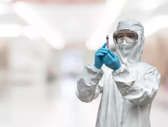
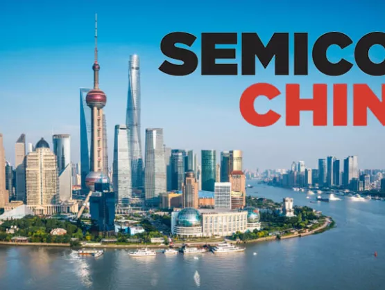
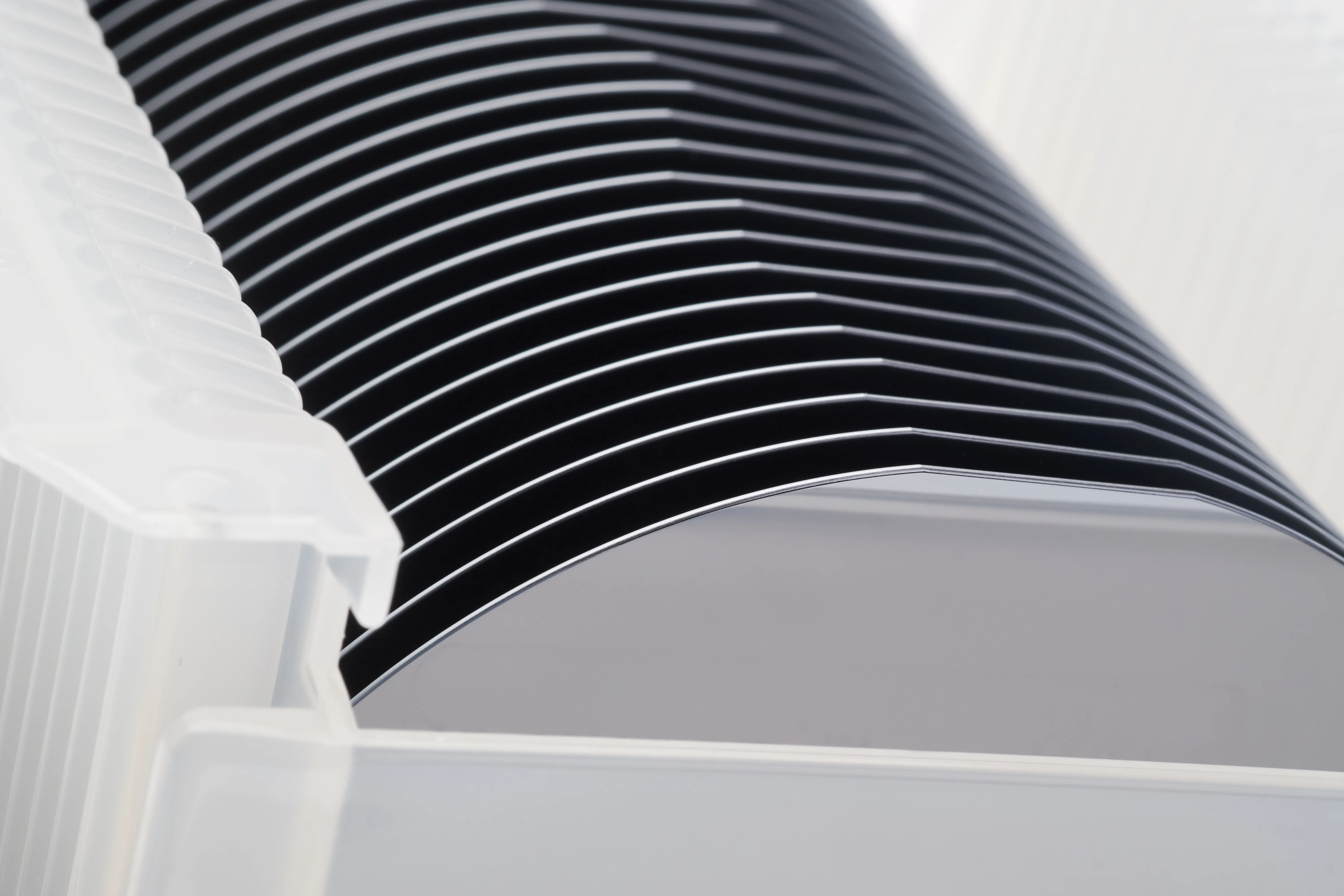
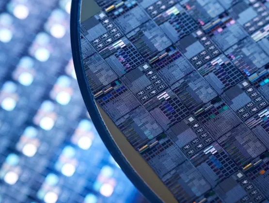
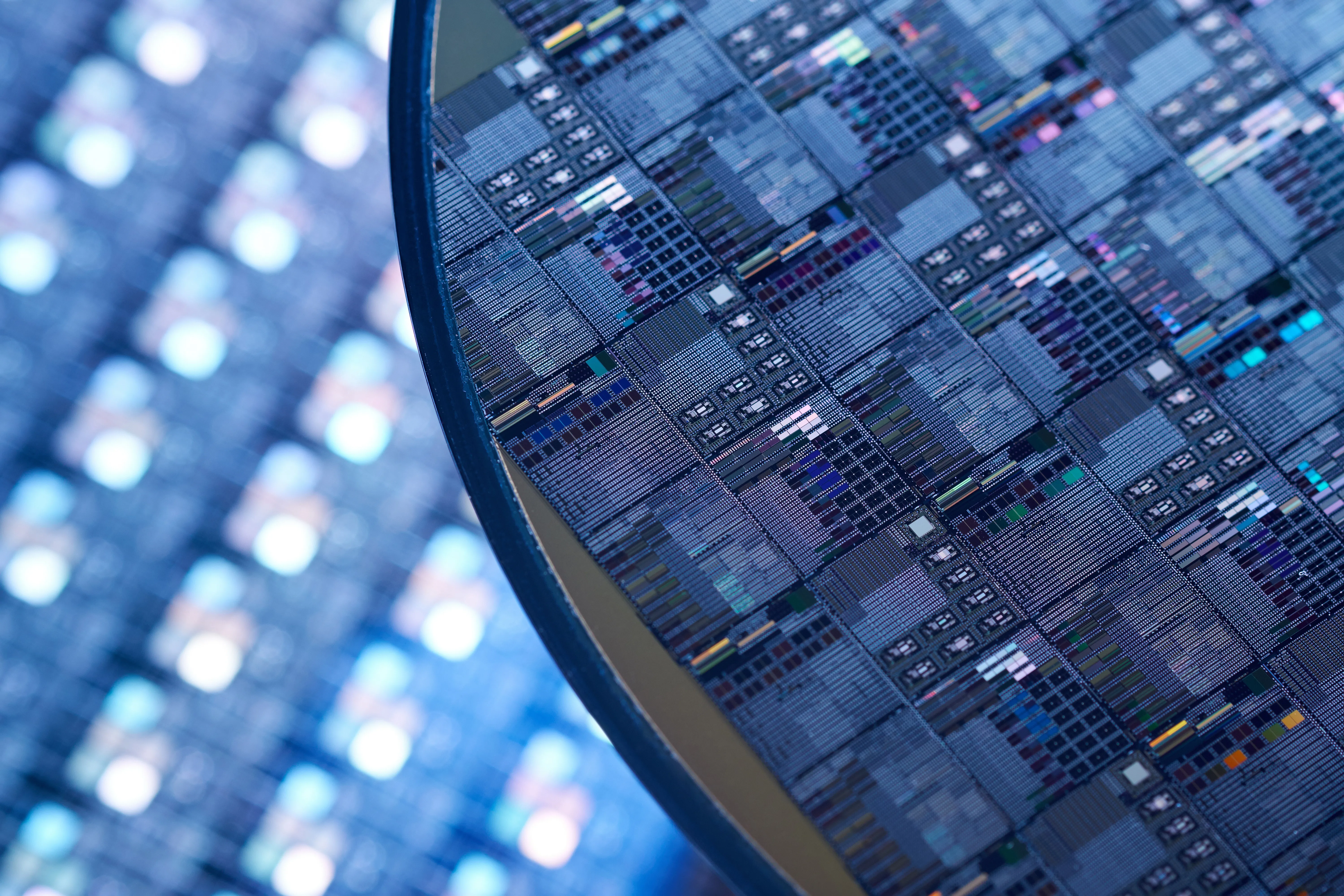
In the two months since the COVID-19 outbreak in January, the Chinese economy has shifted from shock to ongoing recovery under the guidance of the Chinese government. China has worked tirelessly to restore production at its chip manufacturing facilities, a core strategic industry in the region, and the effort is paying off. Operations at several fabs and OSATs – the domestic semiconductor industry’s chief growth engines – have begun to stabilize.As of mid-March, SMIC had restored its manufacturing lines to over 90% of production capacity and expects to be operating at full bore in the next few weeks, while the company’s R D line has returned to full operation. Huahong Grace reestablished normal supplies of various equipment parts and production raw materials. At Huahong Fab2, 12 new pieces of equipment went online to help increase production capacity, and production at Huahong Fab1 and Huahong Fab3 is now stable. JCET said the company's overall return rate has exceeded 90%. Meanwhile, IDM maker Silan Microelectronics' 6-inch and 8-inch lines maintained 90% production.Production lines at Huahong Group, SMIC, CanSemi, GTA Semiconductor, Samsung (Xi'an) and other mainland China chip manufacturers have been generally operating at normal capacity since the Spring Festival. Lines at YMTC, Tianma, CSOT, and BOE, all in the Coronavirus epicenter of Wuhan, have also returned to normal operations. China’s chip industry is finding its footing, and an impressive host of semiconductor companies are gearing up to participate at SEMICON China 2020, rescheduled to June 27-29. The list includes the major domestic wafer foundries such as Huahong, the major packaging and testing companies such as JCET, TFME, Huatian, and large domestic and foreign equipment companies, among them TEL, ASMPT, DISCO, ULVAC, VAT, ASML, KLA, NAURA, AMEC, Anji, CETC, Sinyang, SMEE, CAS, CANON and SPIROX.DigiTimes, a daily newspaper covering the semiconductor, electronics, computer and communications industries in Asia, interviewed SEMI China President Lung Chu in mid-March about what’s ahead for China’s semiconductor industry. Following is an English translation of the interview. DigiTimes InterviewAs China continues to ramp back up to normal activity, SEMI China is making every effort to hold SEMICON China 2020, a leading international semiconductor industry platform for promoting growth and innovation in China's semiconductor industry supply chain. SEMI China president Chu emphasized that the strong support of SEMICON China 2020 exhibitors and the Chinese government made rescheduling the event to June possible.Chu, a semiconductor industry veteran who has experienced numerous economic and industry upheavals over his career including the SARS shock in 2003, said current global economic uncertainty stems from two black swans – the global COVID-19 pandemic and how long it will take to contain it, and the sharp drop in oil prices triggered by the recent geopolitical dispute between Russia and Saudi Arabia. In China, the government responded with strict containment actions and promoted public awareness of self-isolation, resulting in effective domestic containment as of mid-March. As a major oil consumer, China sees the lower prices as relatively favorable to its economy. Those dynamics should allow China to recover sooner than many other regions, and it could emerge even stronger once the pandemic is contained, despite the current slump in global semiconductor demand, Chu said. Once the epidemic has passed, China is in a position of "turning crisis into opportunity," and the semiconductor industry will recover from the trough, he said. Companies in semiconductor supply-chain sectors face various challenges in restoring normal operations. IC design companies experienced relatively low impact since employees can work from home and most companies are located in major cities in China, where epidemic prevention control is strict. For most chip manufacturers, production has not stopped but is hampered by manpower shortages from restrictions on employees returning to work. IC packaging and testing companies are suffering bigger impacts because of the more labor-intensive nature of their operations. However, all companies in the supply chain will be affected by the decline in demand for electronic products and ICs in 2020. As the COVID-19 threat recedes in China, the region remains unwavering in its commitment to semiconductors as a strategic industry with its continuing efforts to evolve sustainable and reliable localized supply chains, Chu said. Investments in “new Infrastructure” for 5G, the Internet of Things (IoT), data centers, as well as public health services should help drive semiconductor demand for smart applications and devices associated with the new infrastructures as are all powered by ICs, benefiting companies in the global supply chain. The COVID-19 outbreak triggered a slowdown in new factory construction after the Chinese government implemented restrictions on the flow of people resulting in a worker shortage. SEMI has revised downward its forecast of wafer equipment spending in China to just a 3% increase this year.Market analysts revised downward forecasts for 2020 annual global semiconductor revenue growth from 7-10% to 0-5%, while some expect negative growth. The recent COVID-19 outbreaks in Europe, the United States and other regions have created more uncertainty. Declining end-user demand for electronics will drive down spending on upstream equipment for both memory and logic IC device makers. For Chu and his SEMI China staff, the postponement of SEMICON China 2020 has been a “major challenge,” he said. “It is a huge project to communicate and coordinate with the government and to reconfirm with exhibitors and industry leaders.”As a leading industry platform, SEMICON China attracts a large number of global customers and suppliers each year. The major China domestic suppliers, leading foundries and OSATs have confirmed their attendance in SEMICON China 2020. Most key foreign suppliers are planning to staff the event with local teams in case some executives are unable to enter China by June due to travel restrictions if the COVID-19 virus has not been brought under control in the United States, Europe and other regions. To assure the success of the concurrent Forums, SEMI has prepared multiple contingency plans, including live broadcast, video and slide presentations. SEMI will also hold the grand opening session at a larger venue than last year’s event to accommodate more attendees with more sitting distance apart. SEMI will follow government guidelines to implement appropriate public health and safety measures during SEMICON China. "Ensuring the welfare of all exhibitors and guests and providing a safe exhibition environment is SEMI’s top priority," Chu said.Cherry Sun is a marketing manager at SEMI China.
Read More
Famous for its warmth and hospitality, Japan always welcomes visitors from around the world with a gracious embrace. But when is the best season to visit? It depends on the interest of each visitor of course. For Instagrammers, the April cherry blossoms or November autumn leaves – a masterpiece of art with their rainbow gold, red and yellow hues – are ideal for snapping memorable pictures. For foodies, winter delights with tuna, toro sushi and other seafood at their tastiest. Wagyu peaks in richness, too, when the cold weather sets in. For anime and manga enthusiasts, August is definitely the time to visit. That’s when COMIKET, the world’s largest comic market – drawing more than a half million people – takes place in Tokyo. But for people in the electronics value chain, the perfect time to pack their bags and hop a flight to Tokyo is December, when SEMICON Japan – December 11-13 at Tokyo Big Sight – opens its doors with its own form of hospitality.Why should you attend? Here are the five top reasons.Reason 1: Japan is home to leading electronics industry suppliersAccording to VLSI Technology, seven of the top 15 semiconductor equipment suppliers in 2018 are headquartered in Japan, and many Japanese companies also lead backend equipment segments. For decades, Japanese companies have supplied about one third of the equipment for the global semiconductor equipment industry, according to SEMI and the Semiconductor Equipment Association of Japan (SEAJ). Most of these companies typically set up a booth on the SEMICON Japan show floor to welcome your visit.True, many Japanese suppliers also exhibit at SEMICON shows outside of Japan to meet with customers. But you will find many more engineers, managers and executives of equipment suppliers on their home ground at SEMICON Japan, where suppliers typically debut new equipment. Their booths are also ideal locations for visitors to meet with suppliers to ask questions, exchange opinions and negotiate new business deals.Japanese materials suppliers enjoy an even larger market share, providing about half the materials for the global semiconductor industry. These suppliers dominate in silicon wafers, photomasks, photoresists, sputtering targets, packaging substrates, bonding wires, leadframes, mold compounds and wafer level packaging dielectrics. Unlike equipment suppliers, not all materials companies exhibit. Instead, many participate as speakers and attend to connect with customers.Reason 2: Get ready for the next semiconductor industry upturnA year ago, in late 2018, we expected chip inventory to stabilize by mid-2019, yet the industry still struggles with high inventory overall and low average selling price for memory. The SEMI 2019 equipment billing forecast was lowered accordingly from -4.0 percent growth (2018 year-end forecast) to -18.4 percent (2019 mid-year forecast). However, the two forecasts still predict positive growth in 2020. As SEMICON Japan 2019 is underway, we should be at the beginning of the next upturn.The chart below shows that more wafer process fabs will start construction in 2020 than this year. (Please see article: Nearly $50 Billion in Fabs to Start Construction in 2020.) Custer Consulting Group also pointed to “a resumption in semiconductor chip and capital equipment growth in late 2019 or early 2020.” (Please see article: Semiconductor Industry Upturn by Early 2020?.)With better times ahead, SEMICON Japan 2019 will be an opportune time to exchange opinions with key players across the supply chain and start negotiations for the coming robust recovery of the equipment, components and materials markets.Reason 3: Glimpse the future at SuperTHEATERSEMICON Japan SuperTHEATER will feature industry and technology insights from global visionaries. Asako Eda, Japan’s chief representative officer of the World Economic Forum and the former president of Intel Japan, will open the SuperTHEATER with her keynote on how we live in an era where the fourth industrial revolution, climate change, disparity and geopolitical risks are affecting our lives and with the speed we have never experienced. She will explore the growing role of innovation and social responsibility and how the World Economic Forum is addressing associated challenges. The opening keynote session will also feature Nandan Nayampally, vice president and general manager of the Immersive Experience group at Arm.In all, the SuperTHEATER will host seven keynote forums over three days at SEMICON Japan including: Semiconductor Executive Forum – Terushi Shimizu, representative director and president of Sony Semiconductor Solutions, and Atsuyoshi Koike, president of Western Digital Japan, will discuss their business strategies and prospects. Manufacturing Innovation Summit – Executives from Applied Materials, KLA, Nikon and Tokyo Electron will discuss business and technology issues as well as innovations that will drive growth to 2030. All seven SuperTHEATER programs will be simultaneously translated to English for international audiences.Reason 4: Connect to application communitiesCollaboration across the value chain has never been more important to industry innovation and growth – the very reason SEMI has expanded its reach beyond the semiconductor manufacturing supply chain (equipment and materials) to include design, systems and products.The SEMICON Japan show and conferences will connect you to key application segments of the value chain. The SuperTHEATER will host two SMART transportation forums highlighting the latest developments in autonomous driving and sky transportation (flying cars). In the SMART Applications Zone on the show floor, you’ll find electronics products and technologies showcased for automotive and manufacturing automation as the autonomous driving pavilion highlights emerging technologies that are driving semiconductor innovation opportunities. Reason 5: Learn from disaster and recovery experiencesJapan has taken important disaster recovery lessons from devastating earthquakes over the past three decades, most notably the Kumamoto quake in 2016, the Tohoku temblor in 2011 and the Kobe rattler in 1995. So has the Japan electronics supply chain, including SEMI members. In the Business Continuity Plan (BCP) area at SEMICON Japan 2019, exhibitors including DISCO, Murata Machinery and THK will highlight technologies that can strengthen your preparedness for a disaster and aid in the recovery.On December 12 at the BCP seminar at Japan 2019, Sony Semiconductor Manufacturing, DISCO and Team Engineering Consulting will share their experiences and expertise in mitigating the disaster impacts. (Sony and Disco will present in Japanese.)To get the feel for the magnitude of a major earthquake and how seismic isolation protects against structural damage, be sure to take advantage of THK’s earthquake experience car. Seismic isolation installs isolators – rubber bearings, friction bearings, ball bearings, spring systems or other devices – beneath a building to buffer earthquake vibrations transmitted to structures.More reasons to attend SEMICON JapanAnd of course your visit to Tokyo for SEMICON Japan 2019 wouldn’t be complete without exploring Tokyo and other regions to experience Japan’s exotic culture, cityscapes and cuisine! Here are some resources to give you even more reasons to book a flight to Tokyo: Japan National Tourism Organization Go Tokyo Kyoto Tourism I look forward to seeing you at SEMICON Japan in December!Jim Hamajima is president of SEMI Japan.
Read More
This article is the fourth in a series highlighting the vital importance of SEMI Standards to commemorate the publication of the 1000th SEMI Standard in July 2019. Find the entire series here.Computer prices have plunged over the years even as desktop and laptop PC performance has skyrocketed thanks to the semiconductor industry, giving users much more bang for their buck. The chip industry stands in a stark contrast to healthcare and education with their exponentially rising costs.What distinguishes the semiconductor industry from healthcare and education in the capacity to deliver so much for so much less over time? After all, even in other parts of the technology sector that are heavily regulated, such as cable television, we have not witnessed the same price decreases as in microelectronics.Some pundits claim that the difference among sectors is tied to their degree of regulation. Does greater regulation somehow degrade product value? The reality is far more nuanced. But one thing is clear: Smart self-regulation (i.e. standards) in the semiconductor industry has contributed mightily to its success.The recipe for success has been simple. Standards have been rocket fuel for competition, which in turn has sparked innovation, driving down device prices while boosting performance. Computer prices fell dramatically between 1997-2015 while the cost of cable TV and internet services rose. Myth of unregulated competitionA semiconductor fab might actually be the most regulated place on earth. Fabs hew to a much higher standard of air quality and cleanliness than even uber-sterile hospital operating rooms. Manufacturing processes are voluntarily regulated not to millimeters, but to nanometers. While some standards are proprietary with limited reach, others span the supply chain. Regulation has worked so well in this sector that the semiconductor industry isn’t moving toward less standardization. It’s moving toward more. Secret is smart standards The gap between regulation and self-regulation is more like a chasm. We typically view regulation as a series of top-down directives that more often focus on the interests of the producer than the consumer. Healthcare regulation, for example, may improve quality of care, but it’s often insurers, big pharma and hospitals that benefit most from regulation, rather than consumers.The semiconductor industry, on the other hand, uses self-regulation to improve business operations and make better products for consumers. Falling prices and rising performance are natural byproducts.Semiconductor industry self-regulation is an ecosystem-wide effort, where input isn’t just top-down, but also bottom-up or even side-to-side. The first SEMI Standard, which specified wafer sizes, exemplifies this approach.The SEMI Standards Committee formed in 1973 to address silicon wafer dimensional specifications. At the time, wafer specifications proliferated. Numbering more than 2,000, the various specifications led to major inefficiencies just when the industry was just getting underway. Wafer suppliers banded together under SEMI to solve this problem and rapidly developed consensus specifications for 2- and 3-inch wafers. By the mid-1970s, over 80% of wafers conformed to these new standards.Standardized wafer sizes freed equipment companies to focus on innovations that reduced cost and increased performance. It also allowed manufacturers to focus on product differentiation without having to worry about device fabrication process and cost. Since that first SEMI Standard made possible the modern semiconductor equipment industry, original equipment manufacturers (OEMs) have competed to deliver amazing innovations. For example, lithography systems routinely use light to design chips with feature sizes smaller than the wavelength of light.SEMI’s 1000th standard on energetic materials demonstrates how smart standards are also pragmatic. This standard is not about banning materials or assigning blame when things go awry. It is about creating practical guidelines that companies will follow, enabling them to realize greater innovation. Guidelines that reduce accidents and risks will spur more, not less, energetic materials’ exploration. Industry suppliers will be the big winners.The 1st to the 1000th SEMI standard all represent examples of cooperation making more sense than competition.Standards for the real worldCreating a business-friendly standard that still gets the job done is a process. As SEMI Standards Task Force and Committee members, materials, equipment and manufacturing companies take part in defining best practice guidelines that support safe and practical use of materials and equipment. Task force and committee members assign particular responsibilities and associated costs to the most logical segments of the supply chain. They also develop information-sharing practices around competitive process recipes and purity standards.Andy McIntyre, CIH, a member of the energetic materials task force and an executive vice president and managing principal at BSI EHS Services and Solutions, summarized what makes SEMI standards smart.“SEMI standards are pragmatic,” said McIntyre. “They take into account the need for implementation in a real-world business environment. They embrace an engineering approach to problem-solving to create practical solutions, and they define specifications and performance goals in ways that allow engineers — in collaboration with EHS professionals — to identify practical solutions for reducing risk in R D, pilot line and manufacturing operations.“SEMI standards employ a holistic process that considers all the important points of view throughout the supply chain, from materials selection, installation, use, recycling and/or disposal,” said McIntyre. “The breadth of SEMI EHS Guidelines, for example, is also very comprehensive as the SEMI EHS Committee and task forces work to ensure that standards keep pace with dynamic technology developments. Energetic materials is a prime example where the industry recognized the need for a new safety guideline to document safe usage of pyrophoric, water-reactive and unstable reactive materials, which have become increasingly important in semiconductor and advanced materials R D and manufacturing.”This is the real secret to the success of the semiconductor industry. Smart self-regulation allows industry players to cooperate in the development and implementation of standards that are pragmatic, comprehensive and dynamic. Participants in SEMI Standards have a voice in the semiconductor industry because they are the voice of the semiconductor industry.While innovation in semiconductors may not always keep pace with Moore’s Law, we can depend on one truth: As long as collaboration and cooperation are the rule and not the exception, we will continue to advance technology in amazing and unprecedented ways. You, me and all other consumers will continue to reap the rewards of innovation. Use your voice to affect standardization in and around the semiconductor industry. Learn about SEMI Standards – and become part of the solution.Heidi Hoffman is senior director of technology communities marketing at SEMI. Hoffman and her team shine a spotlight on the work of the more than 20 technology communities under the SEMI electronics manufacturing supply chain collaboration platform. Actively engaging community members in marketing programs that showcase their unique value, Hoffman’s team helps companies to grow and prosper through the power of connection, collaboration and innovation.
Read More
Semiconductor fabs have been getting smarter and smarter over the past 30 years. It’s a natural evolution – the direct outcome of numerous continuous-improvement efforts. The really important difference on the road to smarter fabs, the one change that’s enabling the Industry 4.0 revolution, is the concept of a cyber-physical system or digital twin. If you don’t have a thorough, detailed, high-fidelity digital twin of your entire fab operation, then you cannot have “Smart Manufacturing.” That’s really the definition of a smart site. A digital twin is simply a requirement for all smart factories of the future. One caveat: No matter what you build today from a smart perspective, your digital twin’s fidelity will improve over the next 20 years. A factory’s digital twin has two facets: the operational aspect and the yield aspect. Each of these two facets places different requirements on a database including the types of data, the frequency of data generated, the retention of data, and even the AI/ML techniques used to analyze the data. A combination of these data requirements are needed to create a digital twin – the virtual representation of your entire factory operation, whether it’s on the wafer-fab front end or the assembly and test back end. What’s most important here is that facility-wide data sets and databases must be able to communicate with each other using refined summary statistics to create a practical digital twin. For example, a lot of information is collected on the yield side to feed the deep-learning models needed to manage processes. However, the factory scheduler, driven largely by the smart operational database, needs only summary statistics from the yield database to be able to act in the next moment or over the next 24 hours. Figure 1 illustrates the needs of and the interaction between a smart operational and a yield database. Figure 1: The Operational and Yield databases in a Smart Factory need to exchange summary statistics. Today, we find that although these databases generally speak to each other in smart factories, they’re still not sufficiently connected to permit the use and analysis of data needed to realize the full potential of a smart factory. That level of interconnectedness is still in the future. Some solution providers have created what is essentially a “smart learning warehouse” (“database” has become too limited a term here). This warehouse collects, analyzes and learns from the extensive amount of information that a fab generates. Game-changing, more holistic applications become possible when this information can be combined in new and informative ways. As it turns out, a data source is just a data source, but users in different factory areas need to extract different information from these common data sources. They need different applications and portals – in other words “views” – that are adapted and adjusted for each area’s needs. Aren’t we smart enough? Some people think that 300mm fabs are already smart. That’s true. They are. But, they could be a lot smarter. No 300mm fab in use today has attained the full, utopian vision of what a smart factory can deliver over the next 10 years. When you finally integrate all of the disparate databases in a fab – when you’re able to use all of those different data sources as one common data source – that’s when your Smart Factory will have the ability to self-optimize its future actions and react quickly to real-time events. The largest semiconductor manufacturers tend to develop these smart factory applications on their own. The remaining semiconductor fabs need to work together with other fabs and their solution providers to develop these smart factory applications. Why now? Why is everyone talking about “Smart” now? It’s because the semiconductor industry has helped to create all of the enabling technology: the compute power, the networking and networking standards, and even the industry’s maturation into a multi-tiered organization of solution providers. We’ve reached the point where we can collect data from a widespread sensor network along with tool-health data and we can then warehouse this data so that it can be applied to more intelligent decision-making. While there may be one or two sensors on a tool today, in the future there will be many such sensors connected over an IoT network or networks that provide mountains of data to the warehouse. All of this data will feed into the digital-twin version of the fab. One of the biggest changes on the horizon made possible by all of this accessible data is advanced scheduling. Despite all of the automation advancements made over the past 25 years, including robotic handling, it’s still hard to decide “where, what, and when?” for every single lot in the factory. Today, no factory in the world is more complex than a semiconductor fab. Optimizing a semiconductor manufacturing process is the most complex manufacturing-optimization task in the world. Do it for ROI ROI is the chief reason for having a digital twin. Once you can make a truly smart, holistic schedule of the fabs operations — not a dispatch or rule-based dispatch list — then you can create an operationally smart factory. Rule-based dispatching systems primarily focus on tools and tool-centric views. Although they incorporate knowledge from current WIP and tool conditions to make decisions better than simple dispatch systems, smart factories are not just about tools and the current WIP at them. Smart factories use the status of every tool and lot in the factory to make fab-centric optimizations instead of tool-specific optimizations. Once you have a digital twin, you’re optimizing for global functions such as line linearity and on-time delivery. These functions are not just about the moment. The transition to a smart factory thus represents a huge philosophical change. When you know exactly what’s going to happen in a factory over the next 12 hours for every single lot, every single wafer carrier, and every single entrance port of every tool in the factory, then you suddenly have control over the factory’s idle time. You know when you can optimally perform PM (preventive maintenance). You know how to best redirect material or labor resources to maximize output. You can create a smart schedule for every maintenance person in the factory that comprehends each person’s skill set and tool downtime so that there’s no negative impact on the factory’s productivity. You can only do all of this when you know the future. Figure 2 illustrates the opportunity. Imagine that a factory contains 1,500 tools. Use of these tools is scheduled for the next twelve hours. The information depicted in Figure 2 encompasses process changes from one chemistry to another, implant changes, reticle changes, and the status of every single consumable for all 1,500 tools. The white spaces that appear between processes in Figure 2 represent opportunities to intelligently schedule events such as maintenance to maximize factory productivity. Figure 2: Smart scheduling permits factory-wide optimization to maximize productivity. Once you have a schedule, you need to translate that schedule into actions or movement. It’s not easy to do this and most material-control systems today make overly simplistic decisions based on modeled assumptions and typical cases rather than the actual time each lot needs to be at a precise location, which can only come from a schedule. Once the data from all of the tools is connected, a smart scheduling system can use the digital twin to make far better process decisions. The larger the factory (or more complex the factory), the more important it is to make smarter decisions. Note: SEMI has a Smart Manufacturing Technology Community. For more information or to get involved, click here. If you would like to discuss Smart Manufacturing more with John directly, he can be contacted at [email protected]. John Behnke is general manager of the Final Phase Systems product line at INFICON.
Read More
IC design has emerged as the largest semiconductor sector in China, with 2017 revenues of $31.9 billion generated by about 1,380 companies. At the same time, China’s fabless segment has risen to third in global rankings with about one-tenth of worldwide sales.Most of China’s fabless segment produces the logic chips that are key to defense, telecommunications, finance and other industries important to the region’s national security interests and its independence from U.S. and other international suppliers. Investment in fabless logic continues to be the top priority in China’s Phase 2 investment. In mobile, China made meaningful progress through HiSilicon and Spreadtrum, both fabless design houses.In 2017, HiSilicon and UNISOC (formerly Spreadtrum), China’s two largest domestic IC design companies, were ranked in the global top 10 of fabless companies, though most Chinese IC design companies are small, with revenues under $1 million. Working with domestic smartphone makers, both companies have carved out a strong presence in logic and, in particular, the communications and application processors that power data centers and Internet of Things (IoT).Despite their rapid rise, China’s AI accelerators and cryptocurrency ASIC suppliers have yet to appear in China’s top 10. However, we expect their aggressive roadmaps and early adoption of leading-edge process technologies to propel them into the top 10 in the near future. As illustrated in the figure below, an examination of the competitiveness of China’s semiconductor segments reveals that the close proximity of China’s fabless companies to the region’s electronic systems makers plays to their advantage, though access to IP and leading-edge process technologies is a barrier to their growth in the near term. A key barrier to China’s foundries is their limited ability to develop leading-edge process technologies and strategic relationships with top international fabless companies. Most leading international fabless companies rely on customer-owned tooling (COT) and design tools for design. As the approach takes time to develop, it will not support China’s aggressive goal and timeline to independently meet domestic IC demand. Instead, China has been disciplined in executing its strategy to acquire valuable IP and leading-edge technologies by aggressively partnering with international fabless design leaders and pursuing deals with market leaders and laggards. The initial entry point for Chinese fabless companies was the low-margin consumer applications dominated by Chinese suppliers, giving them considerable control over demand. In addition, Chinese companies have aggressively hired top talent from abroad and grown the skills of its engineering workforce to sustain innovation. China will likely free itself from its reliance on non-Chinese developed manufacturing process technology and EDA design tools.China’s semiconductor design growth, concentrated in the Pearl River Delta (see figure below), is fueled by national and local investment programs. SEMI August 2018 The Pearl River Delta, which includes Xiamen, Quanzhou and Shenzhen, is establishing itself as China’s IC design, system and application hub. Domestic and international companies are eligible for investment provided they are established or investing in one of the four regionshat are home to various sectors of the electronics and semiconductor supply chain. Access to large investment funds, coupled with China’s infrastructure build-out, is a strong supporting force to drive the growth of top-tier domestic fabless companies. For its part, the Phase 2 of China’s National Investment Fund targets investments of RMB 150 - 200 billion ($23 billion - $30 billion) in IC design. The growing domestic consumer base and infrastructure investment will drive opportunities for China’s fabless companies over the next decade.To learn more about the latest development on China IC Industry, and get a sample of the China IC Ecosystem Report, visit http://www.semi.org/en/china-ic-ecosystem-report.China IC Ecosystem Report covers the rise of China’s IC industry, national and local government policies, public and private funding, and their implications for China's IC supply chain. The report also compares key domestic companies and their international peers segment by segment.Eugenia Liu is a senior product marketing manager at SEMI. Shanshan Du is chief analyst and program director at SEMI China.
Read More
SEMI spoke with Udo Gómez, senior vice president at Robert Bosch GmbH, about MEMS technology requirements relative to standard IC design and manufacturing. Gómez highlighted solutions to challenges of MEMS technology development and manufacturing ahead of his presentation at the 22nd Fab Management Forum at SEMICON Europa 2018, 13-16, November 2018, in Munich, Germany. To register for the event, click here.SEMI: Regarding standard processes for MEMS, the situation used to be known as the MEMS law: "one product, one process." Today, the variety of MEMS sensors and their application requirements have drastically increased. What is the status of process standardization today?Gómez: Today, standardization in MEMS is certainly not as advanced as it is for conventional semiconductor processes and model environments. However, MEMS technology has developed very much in recent years. The understanding of the numerous interactions between mechanical, chemical and electrical parameters has grown enormously. Improved process tolerances and optimized simulation tools already allow the design of standard components and their manufacture using largely standardized processes and systems.This also enables standardized MEMS process platforms in foundries for fabless suppliers, since adapting process parameters to standard designs no longer means maximum effort. But the situation changes significantly if you want to implement more powerful MEMS components for demanding applications. In this case, much effort is still required in technology development to bring new and innovative designs to mass production readiness.SEMI: How does this situation interfere with the need for a fast, market-driven product development and production ramp-up?Gómez: The constant advancement of (MEMS) technology to new limits requires enormous efforts and time. Thus, fast product cycles in consumer electronics (CE) pose particular challenges. Close interaction between product and technology development is a key success factor here, as well as a deep understanding of the cause-effect relationships. This is the only way to identify and minimize process risks at an early stage.However, the steep product ramp-ups usually required in CE also offer advantages, since learning curves are run through at much shorter time-intervals than, for example, the comparatively slow ramp-ups in the automotive industry. In this way, automotive products benefit directly from the results of CE components. Conversely, CE products benefit from the higher requirements in the automotive sector, whose technologies can be developed and tested on longer time scales.SEMI: What are the critical and different design and manufacturing requirements for MEMS products versus standard IC products, which typically run in highly standardized processes?Gómez: A very special feature of MEMS devices is their multi-physics character – mechanical, electrical, magnetic, fluidic, and even chemical and/or optical effects may play a role. This is very different from standard semiconductors. Depending on the type of sensor or actuator, dedicated and often quite sophisticated models need to be developed to ensure proper function of the device – and not least to ensure full functionality after misuse. For example, shocks or drop events are usually not relevant for standard ICs but they may be extremely relevant for MEMS devices with their fragile mechanical structures.Similarly, the influence of packaging effects like bending or thermomechanical stress may be much more significant in MEMS devices than for standard semiconductors. And last but not least, a physical/magnetic/chemical/optical … stimulus usually needs to be applied when testing MEMS devices. All of this adds complexity to the manufacturing flow and requires dedicated know-how both during the engineering stage and in mass production.SEMI: BOSCH is working to extend the process platform to include complex 3D structures. What are the advantages and benefits of using 3D structures compared to standard 2D structures? Are there 3D structured products already in mass production?Gómez: We have recently extended our well-established surface micromachining process for MEMS inertial sensors (which basically uses one functional silicon layer for the movable MEMS device) to an advanced process using a second functional micromechanical layer. This opens up a large variety of design options and allows the realization of entirely new sensor topologies. For example, our most recent z-axis accelerometers for automotive and CE applications have 3D-like structures for the movable mass.This has several advantages: Firstly, the sensors can be further miniaturized as they now have fixed electrodes for capacitive readout above and below the movable mass, i.e. a larger capacitance per area. Secondly, due to their improved symmetry, these sensors have greatly improved immunity against several parasitic effects, e.g. mechanical stress from soldering or bending on a PCB. Overall, this technology enables us to offer better performance at still very competitive product size and cost. Both automotive and CE sensors are in high volume production for different applications and customers. SEMI: What do you expect from SEMICON Europa 2018 and why do you recommend attending the Fab Management Forum?Gómez: After our very positive impressions of SEMICON Europa 2017, we are convinced that SEMICON 2018 will again meet with widespread interest within the semiconductor industry. SEMICON is an excellent opportunity for us to meet our customers and partners. The Fab Management Forum, which ideally takes place parallel to SEMICON, is a highly valuable addition for us to exchange ideas with leading industry partners and to gain new insights into current trends and technical progress. Within that context, the Forum will make a valuable contribution toward strengthening the European position in semiconductor and MEMS manufacturing. As senior vice president of Robert Bosch GmbH, Dr. Gómez heads Sensor Engineering at Bosch Automotive Electronics (AE/NE-SE) in Reutlingen, Germany, the world’s largest MEMS supplier serving the Automotive, Consumer Electronics and IoT industry. Dr. Gómez started his career at Robert Bosch GmbH in 1999 at Corporate Sector Research and Advanced Engineering (MEMS technology) after completing his doctorate in physics. Before joining Bosch Automotive Electronics in April 2018, he worked in various management positions at Bosch and also held the position of Chief Expert for MEMS sensor technology. From 2013 to March 2018, he was Chief Technical Officer of Bosch Sensortec GmbH - a fully-owned subsidiary of Robert Bosch GmbH, responsible for research and development of micro-electro-mechanical sensors (MEMS) for consumer electronics, smartphones, security systems, industrial technology and logistics.Dr. Gómez has served as Deputy Chairman of the Board of VDE/VDI-Society Microelectronics, Microsystems and Precision Engineering (GMM) since 2014 has been a member of the GSA (Global Semiconductor Alliance) EMEA Leadership Council since 2015.Serena Brischetto is a marketing and communications manager at SEMI Europe.
Read More
SEMI met with Heinz Martin Esser, managing director at Fabmatics GmbH, to discuss how existing 200mm semiconductor fabs can master the challenges of a 24x7 production under highest cost and quality pressure by implementing intralogistics automation solutions. The two spoke ahead to his presentation at the Fab Management Forum at SEMICON Europa 2018, 13-16, November 2018, in Munich, Germany. To register for the event, click here. SEMI: Looking at the latest production capacity data for 2018 – it is a 200mm fab boom. Growing demand for analog, MEMS and RF chips continues to cause acute shortages for both 200mm fab capacity and equipment. Do you think this trend will continue the next years or is it only a short term run on 200mm fabs?Esser: We at Fabmatics believe in a long-term trend. The emergence of the Internet of Things and growing digitalization in all areas of life will continue to increase demand for integrated circuits (ASICs), analog ICs, high-performance components and micro-mechanical sensors (MEMS) in the coming years. Many of these semiconductor elements should be produced in 200 mm fabs.SEMI: How does Fab automation contribute to increase capacity of existing, mature 200mm fabs?Esser: We are convinced that fab automation is one of the greatest potentials for older 200mm factories to effectively master increased demand, increasing efficiency, quality assurance and flexibility at the same time. In particular, material flow automation, which is often the missing link between existing equipment in different production areas, can help increase productivity in an elementary way.If you analyze how long valuable tools typically wait for loading and unloading, you can see a direct effect of the intralogistics automation system, which leads to a significantly higher utilization of process equipment by making the material flow independent from human performance. Additional side effects such as reduced cycle time, stable fab flow factor or flattened WIP shafts further increase the contribution of material flow automation to get the most out of existing mature factories. Older does not mean obsolete.SEMI: What are the biggest challenges for a successful implementation?Esser: There is no single challenge when you automate an existing mature fab. Instead, you face a whole variety of challenges you have to tackle, ranging from historically grown non-aligned fab layouts over non-linear material flows and older non-standardized equipment to “automation unfriendly” fab environment. Also you should not underestimate the efforts to overcome the practice manual fab operation people in the cleanroom are so familiar with for many years. Before doing automation you have to think automation, i.e. you have to question all processes to make them ready for automation.SEMI: What are the key drivers to automate a mature fab today: costs, process stability, quality or a combination of them?Esser: This question should be better asked to our customers, but we believe it is a mix of many impacts. Most likely everybody sees the cost reduction at first, but we get more aware of process and performance stability as well as quality requirements – and here our customers’ play the most important role – become more and more focused.SEMI: What do you expect from SEMICON Europa 2018 and why do you recommend attending the Fab Management Forum?Esser: This year SEMICON Europa will co-locate with electronica. So it`s going to be the greatest trade fair for electronics manufacturing in Europe. We will meet innovators and decision-makers across the whole electronics supply chain. The Fab Management Forum addresses a highly topical question that concerns all semiconductor manufacturers not only in Europe - how to handle complexity and enable the necessary flexibility to cope with customers' needs. High-ranking speakers will give an insight into the latest technologies and best practices. I am looking forward to the lively exchange with the participants and taking away new impulses for our business. Heinz Martin Esser is managing director at Fabmatics GmbH, responsible for sales and marketing, customer service and administration. He studied supply engineering at the University of Applied Sciences in Cologne and later earned a university degree in business administration. Serena Brischetto is a marketing and communications manager at SEMI Europe.
Read More
On June 1st, 2018, Toshiba sold Toshiba Memory, Toshiba’s memory business, to an investment group led by Bain Capital. Toshiba Memory was then owned by a consortium of American, Japanese and Korean companies.After the long and tough negotiations, Toshiba Memory moved forward at full throttle, holding a groundbreaking ceremony for its new 3D NAND fab (100,000 WPM) in Kitakami in July and, in September, celebrating the opening of Fab 6 Phase 1 (50,000 WPM). To be sure, NAND memory is a key feature of Japan’s semiconductor industry. But the sector’s reach extends well beyond memory with its rich and versatile product portfolio nourished by active investment.Born in the early 1950s, Japan’s semiconductor industry today boasts more than 30 companies with fabs. Many feature 200mm and smaller wafer lines with legacy technologies, form factors that account for the bulk of the world’s semiconductors and are the oxygen of Japan’s chip industry. Clearly, the world is not built only with the state-of-art 7nm processed chips on the latest generation 300mm lines. Japanese chipmakers are flourishing.Automotive SemiconductorsRenesas Electronics remains a giant in microcontrollers (MCU) and system on chip (SoC) devices for automotive applications. According to IHS Markit, Renesas automotive semiconductor revenue in 2017 reached $3.6 billion while Inineon Technologies and NXP Semiconductors revenues were $3.4 billion and $3.7 billion, respectively. The three companies dominate the global automotive MCU global market. The company recently acquired Integrated Device Technology (IDT), a U.S. fabless company specializing in analog/mixed signal chips, to strengthen its automotive semiconductor portfolio. Renesas operates four volume production fabs, according to the latest World Fab Forecast from SEMI. Renesas’s microcontrollers for automotive applications (Source: Renesas Electronics) Power SemiconductorsWith power semiconductors the chips of choice for boosting the efficiency and performance of motors and batteries used in equipment, demand for the devices is rapidly growing, especially for automotive applications. Power semiconductor companies in Japan are legion and include Denso, Fuji Electric, Fujitsu Semiconductor, Hitachi, Kyocera, Mitsubishi Electric, New Japan Radio, Origin Electric, Phenitec Semiconductor, Renesas, Rohm, Sanken Electric, Sansha Electric Manufacturing, Seiko NPC, Shindengen Electric Manufacturing, Sumitomo Electric Device Innovations, Toshiba and Toyota Industries. The companies account for 26% of global power semiconductor capacity and will spend $317 million for construction and equipping in 2018.CMOS SensorsSony dominates the CMOS image sensors market with 42% share in 2016, according to Yole Développment. To meet growing demand for high-end CMOS image sensors, Sony has acquired several legacy 300mm wafer fabs and retooled them for CMOS sensor manufacturing. What’s more, Sony’s May announcement of its mid-term corporate strategy includes a 1 trillion Japanese yen investment in CMOS image sensors targeted to automotive applications by March 2021.Sony’s 7.42 effective megapixel stacked CMOS image sensor for automotive cameras (Source: Sony Corporation) MEMSMEMS is perhaps the most wide-ranging device market: Every application requires different capabilities and functions. The latest World Fab Forecast report lists 17 MEMS companies in Japan, though three makers of fast-growing RF MEMS, typically known as surface acoustic wave (SAW) or bulk acoustic wave (BAW) filters, are coming to the attention of semiconductor manufacturers. All are familiar passive electronic components suppliers – Murata Manufacturing, Taiyo Yuden and TDK – and all acquired legacy semiconductor fabs to manufacture RF MEMS.Their high-performance radio wave filters make mobile phones usable around the world. Research companies like Yole expect the introduction of 5G cellular mobile communication systems to fuel another wave of growth of the RF MEMS market. Murata Manufacturing’s SAW filters for smart phones (source Murata Manufacturing) Japanese Supply Chain Meets All Different NeedsJapan’s semiconductor supply chain provides one third of the world’s semiconductor manufacturing equipment and more than half of the industry’s materials. But Japanese suppliers also work with small and midsize makers of highly versatile chips critical to enabling the explosion of smart applications.Meet these versatile Japanese suppliers at SEMICON Japan to find solutions to your unique needs and help the world get smarter. Themed “Dreams Start Here,” SEMICON Japan 2018 reflects the promise of AI (artificial intelligence), Internet of Things (IoT) and Smart technologies. Featuring more than 750 exhibitors from around the world, the event is the gathering place to connect the people, technologies and business across the electronics manufacturing supply chain, from semiconductor manufacturing to autonomous cars, robotics and other smart applications. For more information about SEMICON Japan, visit www.semiconjapan.org.Yoichiro Ando is a marketing director at SEMI Japan.
Read More