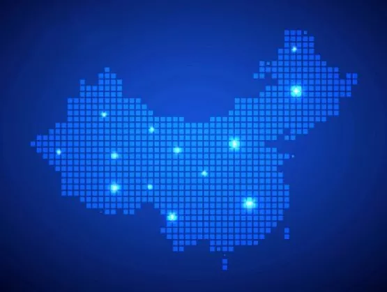
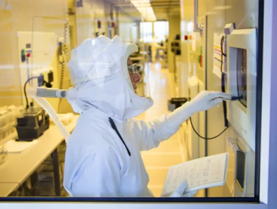
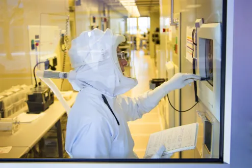
As the world confronts the health crisis of a generation in the form of the fast-spreading coronavirus, the microelectronics industry remains firmly in the spotlight. Aware of the central role they play in the fight against the COVID-19 pandemic, a growing number of companies are joining efforts to combat the virus by developing technologies for coronavirus detection, contact tracing and predicting its spread.SkyWater Technology, a U.S.-based foundry and prestigious member of SEMI-Fab Owners Alliance, is on the front lines in supplying an essential microfluidic MEMS component used in COVID-19 testing and research to identify mutations of the virus. This component is instrumental for the sequencing kit in the DNBSEQ-T7 system, an ultra-high-throughput sequencing system manufactured by MGI, a subsidiary of global genomics leader BGI Group.SEMI had the pleasure to catch up with Thomas Sonderman, president of SkyWater Technology, to talk about the company’s valuable contribution to the detection of COVID-19. He also gave us a peek into its business continuity plan and the safety measures it is taking to resiliently run a 24/7 chip-making operation amid these unprecedented times.SEMI: Tell us about SkyWater's contribution to the detection of COVID-19 and your partnership with MGI?Sonderman: SkyWater has been working with genomics sequencing leader MGI for several years to supply a critical component used in MGI's DNBSEQ-T7, an ultra-high-throughput sequencing system. The component we supply to MGI is a microfluidic MEMS device that uses microscopic channels to help perform very small-scale chemical reactions in the genetic sequencing platform. MGI's DNBSEQ-T7 identifies and monitors possible mutations of viruses, which is important for epidemiologists when tracking how viral illnesses such as COVID-19 spread through human populations.MGI’s sequencing system is used in parallel with its sister company BGI Genomics’ RT-PCR test kit, which is typically used more broadly as an initial screening agent due to its ability to return virus detection results within a matter of hours. Sequencing with the DNBSEQ-T7 can be used to confirm results of the RT-PCR tests that have indicated positive for the presence of the virus and then to perform a full DNA sequence of these positive specimens, which can help track mutations in the virus.DNBSEQ-T7 is important in the fight against COVID-19 as it tracks how the virus changes and enables scientists to look at its genetic sequence like a fingerprint at a crime scene. Their focus is on finding sudden changes in the sequence over time — a mutation. When they analyze available genomes from infected patients in several countries, they can see if inevitable virus mutations are causing associated illnesses that may have different incubation periods, contagiousness or deadliness – all critical dynamics that must be tracked by public health officials during an outbreak such as this.SEMI: What was the path that brought your company to the forefront of this testing?Sonderman: MGI’s DNBSEQ-T7 sequencing system and BGI’s RT-PCR rapid testing kit were among the first officially approved products by the National Medical Products Administration (NMPA – essentially China’s version of the FDA) – to fight the outbreak. MGI’s manufacturing plant, based in Wuhan, was able to fast-track its response, producing and delivering test kits very quickly to many hospitals and disease control centers in Wuhan and other cities in China.As concerns continue to rise about COVID-19 and we strive to flatten the curve, the pressure is on to enable even faster, more accessible testing. On March 27th, BGI’s RT-PCR virus detection test received FDA Emergency Use Authorization (EUA) for use in the U.S. The test works in just three hours. MGI’s DNBSEQ™ T7 sequencers are being used in China and other countries now and will be available in the U.S. starting in Q3. Products from BGI/MGI and affiliates are currently being distributed to more than 70 countries and regions worldwide to assist the global efforts in fighting the pandemic.SkyWater is certified to the ISO 13485 Quality Standard for Medical Devices to support the design, development and fabrication of DNA sequencing and other biochip applications in a wide range of emerging biomedical market segments. This allows us to provide this type of cutting-edge technology solution that is making an important contribution to coronavirus detection.SEMI: Given the challenges COVID-19 has placed on workforce and supply chain, what steps are being taken by your company to mitigate disruptions? Sonderman: SkyWater has been identified as Essential Critical Infrastructure per the U.S. Dept. of Homeland Security in several categories including Healthcare/Public Health Sector, Defense Industrial Base Sector, Information Technology Sector, and Critical Manufacturing Sector. To maintain continuity of operations, we contacted our close market partners as we need their support to continue supply of their starting and manufacturing support materials necessary for us to maintain operations. We asked these organizations to make every reasonable effort to fulfill our order requirements while also following recommended protective measures and are actively monitoring these relationships for possible developments that could be disruptive. By means of their partnership with us, these suppliers, too, are a part of the Essential Critical Infrastructure. Currently, there has been no change in wafer operations or fab utilization during this time of COVID-19.In addition to our sustained operations, our fab expansion is well underway as construction continues. The over 60,000-square-foot facility expansion adds clean room area and infrastructure to support the Department of Defense’s investment in SkyWater to broaden our production capabilities for Strategic Rad-Hard electronics and other complementary technologies. A fab technician in SkyWater’s SkyTech Center, an expansion of its operations to enhance advanced processing capabilities at its U.S.-based and U.S.-owned manufacturing facility. SEMI: What advice would you give to other companies seeking to keep their operations running amid COVID-19?Sonderman: First and foremost, creating a Pandemic Response Team (PRT) was critical for us in planning how to operate and communicate during this crisis. Our PRT updates our leadership team multiple times per week to enact procedures and ensure alignment throughout the organization. We follow CDC alerts and other local, state, and federal government guidelines on how to deal with home and work environments while communicating with all company stakeholders. This is important in providing reassurance of the company’s continued business and details on any potential change in operations.Increasing the frequency of communication with the organization’s supply chain to anticipate any disruptions in service is vital. Also, keeping in contact with customers is imperative to take the pulse of their continued operations during COVID-19. We recommend being flexible and pursuing new paradigms in getting business accomplished, such as telecommuting. In addition, if a company is deemed an essential business, we suggest drafting a letter in advance for employees should they need to prove why they are in transit (to and from work) if transportation becomes severely limited and monitored.Communicating with employees on how operations are changing is crucial. Ensure there is an intranet site that employees can access remotely via laptops or mobile devices that allows for ongoing updates and a way to communicate to all employees as things continue to evolve.We also put several safety measures in place, including: A screening process was set up to take the temperature of everyone entering the building. Site access is restricted for vendors, contractors, customers and other visitors as a default policy. Employee travel is restricted. All employees who can do their jobs from home can stay home. For essential on-site workers, we allow flexible schedules so people can move shifts if needed. Shifts have been staggered so people are not congested at lockers, gowning areas and other places. Physical distancing is required everywhere inside and outside the building. Video conferencing is being used even for participants inside the building. The number of people allowed in conference rooms is limited to comply with physical distancing; some chairs were removed and maximum occupancy signs were posted. Hand-sanitizing stations have been set up. We are providing employees access to masks, gloves and cleaning wipes. Safety measures are posted around the building and cleaning frequency of hard surfaces has been ramped significantly. These safety measures are among several other modifications we’ve made to daily operating procedures. SEMI: Please share some examples of how the SEMI Fab Owners Alliance (FOA) has helped support your business?Sonderman: Our Pandemic Response Team has leveraged the FOA recently by participating in its webinars on COVID-19 to ensure we are using industry best practices. We also use FOA surveys to provide and request information pertaining to COVID-19 practices.We have implemented building entrance protocols (i.e. temperature scanning, restricting access for non-employees) and expanded building cleaning procedures, including increasing the cleaning frequency of specific high-touch items. We have adjusted shift start times to minimize the number of personnel in the change room at the same time and we store each fab worker’s hood in the sleeve of the suit. These last two items resulted from a conversation with another FOA member.Outside of the pandemic, we have leveraged the FOA by participating in its industry-wide maintenance best practices and learning group that meets monthly on maintenance needs, issues and concerns within the industry. This allows us to learn from each other within the semiconductor industry. We have also leveraged this group in sourcing parts and/or parts sharing on tools no longer supported by OEMs.We greatly value the type of cross-organizational sharing and learning the FOA facilitates. It has been beneficial in a number of ways over the years. At this time, the FOA is especially useful when best practices are crucial to enable us and our peers to minimize disruptions, operate with the utmost safety, and quickly adapt to this new environment.SkyWater is a member of the SEMI Fab Owners Alliance, an international group of semiconductor and MEMS fab managers and industry suppliers that meets regularly to solve common non-competitive manufacturing issues and improve their business results. Nishita Rao is a product marketing manager at SEMI.