downloadGroupGroupnoun_press release_995423_000000 copyGroupnoun_Feed_96767_000000Group 19noun_pictures_1817522_000000Member company iconResource item iconStore item iconGroup 19Group 19noun_Photo_2085192_000000 Copynoun_presentation_2096081_000000Group 19Group Copy 7noun_webinar_692730_000000Path
Skip to main content
Default Banner Image

sustainability

Artificial intelligence (AI) is scaling at a pace that is reshaping semiconductor roadmaps, data center design, and long-term infrastructure strategy. AI promises many economic and social benefits; but the growth comes with an escalating demand for power, and energy has emerged as a major challenge.SEMI, as the global semiconductor and electronics association connecting over 4,000 companies, continues to unite the entire ecosystem to “bend the curve” – to maximize AI performance while minimizing power consumption. In a series of successful, sold-out workshops that the SEMI Smart Data-AI Initiative held on this topic, a resonant theme has emerged: sustaining AI progress requires energy-efficient computing with holistic co-design and co-optimization across materials, devices, systems, data transmission, data centers, emerging architectures and software. While this dialog is an important starting point, the ultimate goal is to drive concrete action through collaborative innovation.The AI Energy ChallengeAI training compute for frontier models is growing at an estimated 4–5x per year, driving unprecedented demand for hardware capability and infrastructure capacity. That trajectory has resulted in a global “data center gold rush” and is testing energy availability limits. As model sizes scale exponentially, so too does the energy required to train and deploy them; and power consumption has become a significant limiter to performance gains. Further, this increases heat dissipation, and requires innovations like direct liquid cooling.Modern AI and high-performance computing systems now operate at levels comparable to small cities, with tens of megawatts per installation and a trajectory toward gigawatt-scale data center campuses. Grid capacity—both in the U.S. and globally—may be challenged to keep pace with projected demand. Thus, AI infrastructure is no longer just a technical challenge, but it is an energy, systems, and policy challenge.System-Technology Co-OptimizationContinuous advances in chip and inference efficiency have delivered orders-of-magnitude improvements over many decades. These gains must now be expanded by holistic co-optimization of the entire compute system from silicon technologies to data center to the grid.For example, processors can be made more efficient by customizing them for specific workloads. However, only part of total data center power is consumed by the processor itself. A significant portion is used by data movement, power conversion and cooling. The energy required to move data increases dramatically with distance. Moving bits across packages, boards, and networks can consume far more energy than the compute operations themselves. This makes locality a critical design principle. The opportunity—and necessity—therefore lies in cross-layer optimization: efficient compute, efficient communication, and intelligent power management across the entire system. Not surprisingly, advanced packaging and integration are becoming central to performance. These technologies can enable architectures that tightly couple compute, memory, and I/O—using 2.5D and 3D integration techniques—reducing energy per bit and increasing bandwidth. Photonic interconnects and low-power materials can further lower the cost of processing and moving data.The bottom line is that incremental chip-level gains alone will not be sufficient and energy optimization cannot be siloed—system-technology co-optimization is needed.Hardware-Software Co-optimizationKeeping data as localized as possible depends as much on software algorithms as it does on hardware architectures. The challenge is that the development cycles are mismatched: new software models can be developed in months, while designing and fabricating new hardware can take years. While this cycle mismatch is fundamental, closer coordination between hardware and software developers can significantly improve efficiency. For example, offloading selected functions in the algorithm, including distributed DPUs, and reducing the level of data precision can reduce energy use. Partitioning workloads logically across the hardware/software stack between cloud services and compute-on-edge can also reduce energy appreciably. Further, risk mitigation techniques—for example, building in strategic redundancy—can make future designs more resilient to shifts in software algorithms and models.Diverse Computing ModalitiesWhile AI dominates current infrastructure investment, the future of computing will likely include multiple, diverse computational modalities such as quantum, neuromorphic, photonic and analog computing.Different computational paradigms will be applied where they are most effective. For example, quantum computing is likely to complement—not replace—classical systems; especially for specific classes of problems where it offers exponential advantages. However, progress in quantum computing is tightly coupled to advances in semiconductor infrastructure. Error correction, orchestration, and hybrid algorithms all depend on high-performance classical systems operating with low latency alongside quantum processors. While there is no single silver bullet, system-level design can ensure that multiple computing modalities work together within unified workflows spanning edge, cloud, and exascale environments.Why It Matters What to WatchEnergy will now be a key constraint for AI performance and infrastructure expansion.The evolution of gigawatt-scale AI campuses and their interaction with public energy grids will accelerate – or slow down – AI growth.Data movement, memory bandwidth, interconnect efficiency, advanced packaging and heterogeneous integration will be strategic levers. Enhanced system-technology co-optimization and integration of advanced technologies like 3D ICs and photonics will be critical.Co-optimization across hardware, software, and systems will be required.Future architectures will blend classical and emerging compute modalities like quantum, photonic and neuromorphic.In conclusion, AI has become a defining global force with much promise, but its trajectory will be shaped by technology, energy and infrastructure economics working together. This is a formidable challenge because it requires many diverse players with divergent priorities to collaborate effectively.We invite you to join the SEMI Smart Data-AI initiative to collaboratively address this challenge and help realize AI’s full potential sustainably. Our next workshop in this series will be on September 9 in Silicon Valley – please join us for this exciting event.SourcesSEMI Smart Data-AI Initiative – Future of ComputingEnergy-Efficient Computing for AI and Beyond, SEMICON West, October 2025Sustainable AI Systems, SEMI HQ, March 2026About the AuthorsDr. Pushkar P. Apte is the Strategic Technology Advisor for SEMI Global Lead for the Smart Data-AI Initiative Dr. Melissa Grupen-Shemansky is Senior VP and CTO of SEMI
Read More
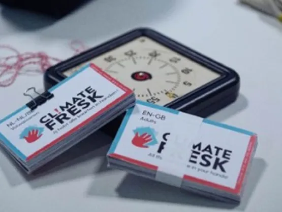
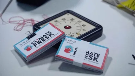
How imec turned a climate literacy workshop into a blueprint for sustainability engagement across the semiconductor industry. The StoryWouter de Groot had spent 9 years at imec in Business Development, a role that kept him airborne across Europe and beyond. Wouter was good at his job, and the travel was part of it. But on a flight somewhere over the Atlantic, his calculus changed.Wouter couldn’t ignore the carbon footprint of his own professional life. He realized, “I couldn’t reduce my travel significantly […] but I could raise awareness.” A seed was planted.In France, Wouter discovered the “Climate Fresk” (La Fresque du Climat), a collaborative, card-based workshop built on science from the Intergovernmental Panel on Climate Change (IPCC). He got trained as a facilitator and returned to imec’s Leuven headquarters with a quiet mission. The first session, held with a small group of HR colleagues in late 2023, was intended as a test. Yet even for that test, what happened surprised everyone in the room:"I was blown away by the depth of the discussions. It wasn't just about facts. It was about how people felt, and what they wanted to do next." —Wim Fyen, Director of Sustainability, imec .custom-quote-block { border-left: 4px solid #d9d9d9; padding-left: 26px; margin: 24px 0; } .custom-quote-block blockquote { margin: 0; padding: 0; border: none; } .custom-quote-block p { margin: 0; font-size: 18px; line-height: 1.6; font-style: italic; color: #000; } 
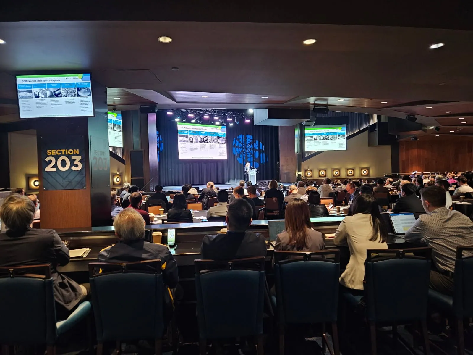
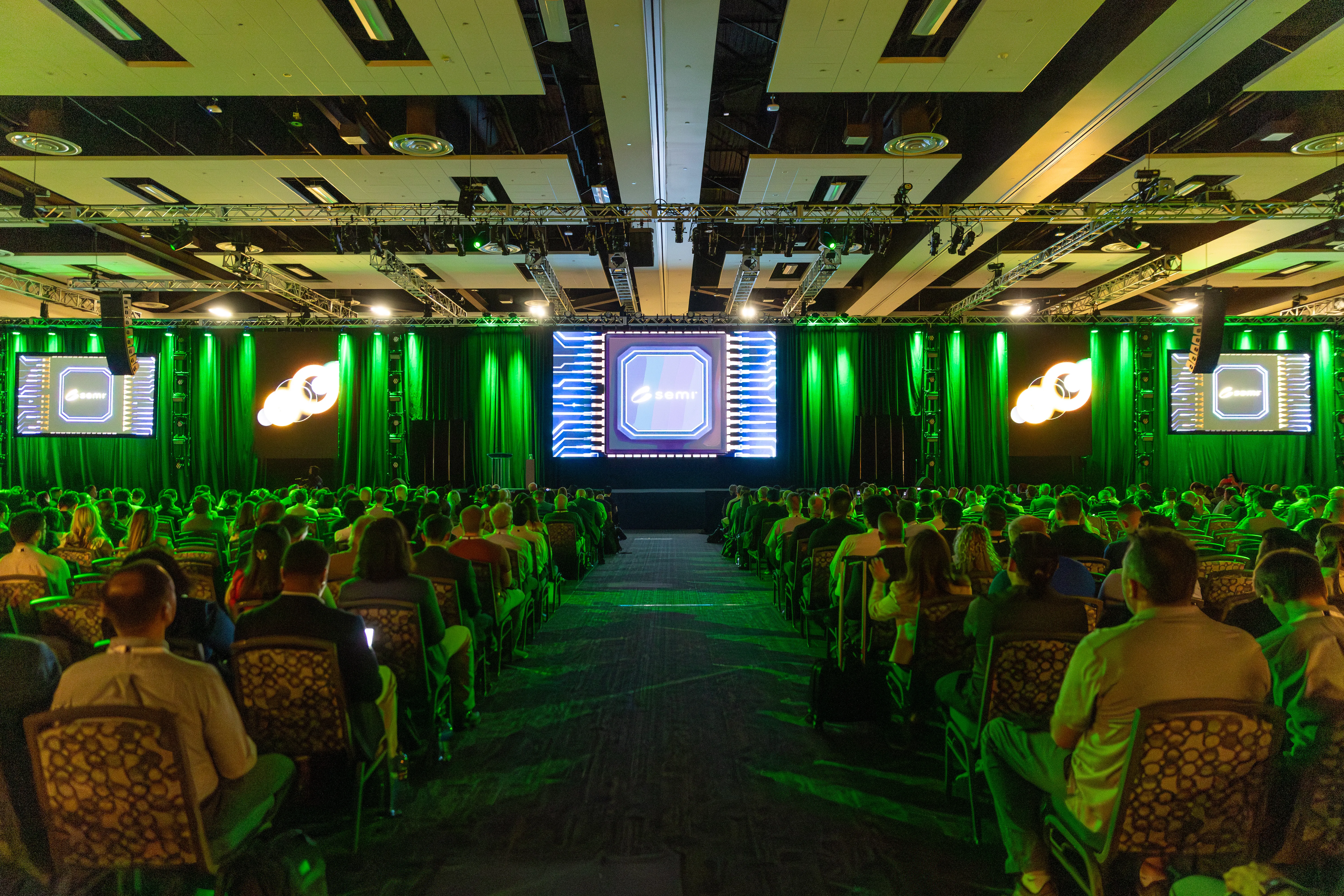
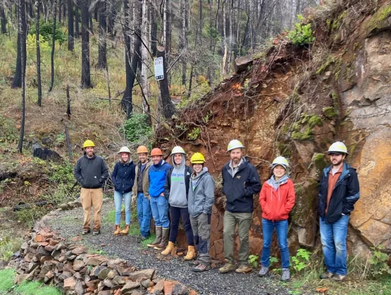
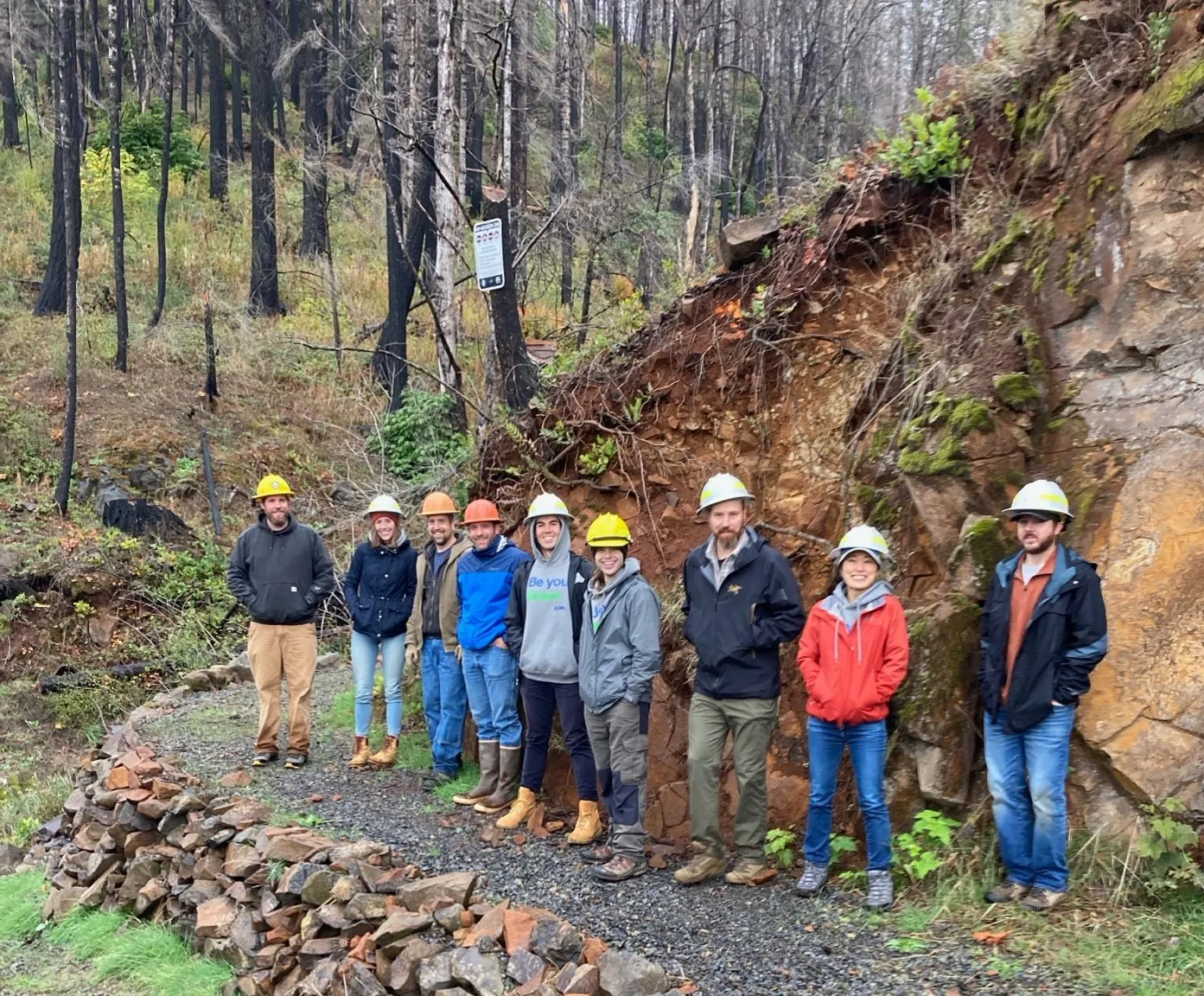
This is the story of those people, the initial hesitations they faced, and the tipping points that firmly established imec’s Climate Fresk movement. The People: 6 Unique Entry PointsBy the time imec presented at the SEMI Climate Equity and Social Impact (CESI) workgroup in June 2025, more than 400 employees had participated. What made it work wasn’t a mandate or a budget line. It was 6 people who found their way to the Climate Fresk from completely different starting points. Without any coordinated plan, they built something unlike anything imec had ever seen. From the 6:Wouter de Groot acted before there was infrastructure in place. Certified with sponsorship from imec, he ran the first session himself and passed it on to anyone willing.Ann-Sophie Vanwinsen, a Procurement Specialist, got certified as a Climate Fresk facilitator outside imec, well before the program was ever offered internally. Vanwinsen has facilitated more sessions than anyone else at the company. She confessed, “I’ve shamelessly taken over using my job for sustainability purposes.”Matthias Nauwelaers from imec.academy felt very emotional during his first session. A graph showing the climate burden falling on future generations hit him somewhere data alone never had. He too signed up as a facilitator and now weaves the Fresk into employee onboarding and e-learning sessions on sustainability.Wouter Machiels, Head of Procurement, came in skeptical. Sustainability, in his experience, had mostly been a compliance checkbox. While Wouter wanted to do more, he felt he lacked the specific tools to act on instincts he already had. The Fresk gave Wouter a framework he hadn’t found elsewhere: “it explained a number of mechanisms I had in the back of my head but couldn’t vocalize.” He left a facilitator himself and has since built a team mapping imec’s entire Scope 3 emissions.Lizzie Boakes, one of imec’s Life Cycle Assessment researchers and a ‘SEMI Europe 20 Under 30’ honoree, described what shifted for her: “I’m usually trying to hit numerical targets that don’t seem very real or human. The Fresk takes the scientific aspects out and highlights the social components. It puts people in a position where they have to be expressive with individuals they’re not necessarily close with.” Boakes became a facilitator, too.Filip Merckx, CFO, felt anger, then urgency, then a sense of responsibility he couldn’t shake. He introduced the Fresk to his entire management team on an offsite and became co-chair of a newly established sustainability board.“Easy in hindsight to say everything was planned, but it wasn’t,” said Wim Fyen, imec’s Director of Sustainability, who served as the connective tissue throughout. “We just went with the flow.”The Hesitation: Bridging Bottom Up and Top Down Senior management valued sustainability, but a 4-hour workshop was a significant ask in a calendar already full. The early response was practical rather than resistant: how do we justify the time? It’s a familiar dynamic. Research on bottom-up sustainability initiatives notes that organizations relying primarily on top-down approaches can miss innovative insights that emerge from employees at all organizational levels (Erzurumlu et al., 2025). Imec found a way around it.Fyen looked for the most efficient way to get it rolled out in imec. He first got the Climate Fresk listed in imec’s learning management system (LMS), a small move that gave it organizational legitimacy without requiring anyone to mandate it. Once the training appeared in the company’s catalog, Fyen leveraged that legitimacy to persuade managers to participate. The budget problem landed differently. Getting the first cohort of facilitators trained required money nobody had earmarked. Machiels solved it by encouraging like-minded suppliers to make sustainable initiative contributions. As a result, the first group got financed without a single line item in the sustainability budget.Both moves mattered. The same research argues that meaningful change requires not only employee initiative but also adequate executive support and corporate financial resources to sustain it (Erzurumlu et al., 2025). The LMS listing supplied the institutional legitimacy. The supplier co-investment supplied the resources. Together they pulled the Fresk from ‘one person’s project’ into something the organization could carry."You train 1 person as facilitator for less than 1,000 euros, and then they can run unlimited sessions inside the company at just a few euros per participant for license fees. Compared to external coaches, it's 30 times more cost-efficient." —Wim FyenThat economics produced a virtuous cycle. Low cost per session lowered the bar for departments to host one. Each session generated interest, which recruited more facilitators, which enabled more sessions. Similar grassroots-to-organizational arcs have played out elsewhere in the industry, where employee-led sustainability initiatives at ASML gained traction once they were paired with executive sponsorship (https://www.semi.org/en/blogs/one-tree-per-employee-how-a-grassroots-initiative-in-asml-san-diego-is-assembling-restorative-future-with-real-results). At imec, the initial constraint of having no dedicated training budget became a feature: it forced a model lean enough to scale. Participants in imec Climate Fresk Workshop for ManagersThe Tipping Points: When Organic Became StructuralWhat came next for imec was a mass Fresk; 50 managers, 14 internal facilitators, 1 afternoon. During the workshop, each participant wrote a personal commitment on seed paper, and those seeds were planted on the imec campus. "The flowers represented their ideas blooming," Fyen said. For a scientific culture, having something tangible to point to mattered. Not long after this, in late 2024, the team of Climate Fresk facilitators received the Sustainable.minds award at imec's annual corporate personnel event, recognized for sparking vital conversations about sustainability and inspiring action for the planet. For a community of facilitators that had grown almost entirely through word of mouth, this formal recognition validated what they had already built and gave their work significant internal visibility.In 2025, entire departments were booking on-demand sessions. About 25% of all participants expressed interest in becoming facilitators themselves. But why? According to a group of French environmental psychologists, emotional engagement is one of the primary pathways through which collaborative climate workshops produce real attitudinal change and pro-environmental intent (Hognon et al., 2026). And the good feeling that follows, which some researchers call the "warm glow," creates a self-reinforcing cycle toward deeper engagement (Schneider et al., 2021)."Convinced that without the information of the Climate Fresk, and without my team having lived through it themselves, we would not be where we are today in value chain mapping and the visibility we have on our Scope 3." —Wouter Machiels, Head of Procurement, imecScaling beyond the borders to impact the entire value chain Fueled by the recognition given by the Sustainable.minds awards, the team began offering Climate Fresk sessions to imec’s partners at the biannual Partner Technical Week (PTW) international conference and the workshop started crossing imec’s borders for the first time. This brought it to the attention of SEMI members. At a CESI workgroup meeting in 2025, participants from Tokyo Electron, Axcelis, Advantest, Applied Materials and Veeco among others listened to imec’s story and asked how to bring it to all of SEMI’s membership. Wojtek Osowiecki at Lam Research, founder of the Lam Employee Sustainability Community, was one of the first outside participants at an imec Fresk. He put it simply: “It’s not just about awareness. It’s about empowerment. The Fresk gives people a voice and a framework for action.” By the Fall of 2025, the first Fresk had been held at SEMICON West, and conversations with SEMI member companies were underway. What had been an internal experiment was now something other organizations wanted to learn from.A Movement of Belonging with Concrete Outcomes Founded in 1984 as the 'chip lab of the world,' imec has always been committed to sustainable development for generations to come by teaming up with the entire microchip value chainIts biggest leverage takes place through its Sustainable Semiconductor Technologies and Systems (SSTS) program in which imec works closely with partners from across the industry to assess and reduce the environmental impact of chip manufacturing, including foundries, integrated device manufacturers, equipment suppliers, and materials companies.This program runs along two connected tracks: assessment, whereby the environmental footprint of current and next-generation integrated circuit technologies are quantified and improvement where the insights of the first track are used to develop and validate practical solutions (e.g. to reduce process-related emissions, including work on low-impact gases, per- and polyfluoroalkyl substances (PFAS) alternatives, and novel manufacturing processes).The success with the Climate Fresk workshop has also begun to feed the broader SSTS program. Tools like the Environmental Score, originally developed for chip manufacturing assessment, are now being integrated into other design processes across the organization. The Fresk is now one of the vehicles imec uses to train and inspire the people who will carry that integration into their day-to-day work; the workshop builds the awareness, and SSTS gives that awareness somewhere to go.And there are several noteworthy concrete outcomes across imec:An ESG board now exists at the executive level, where leaders set corporate sustainability goals and assign the resources to pursue them. That board did not exist prior to the Climate Fresk. It was an indirect consequence of the awareness created within the finance team after Merckx introduced the workshop to his management. Decisions about sustainability that had previously lived in scattered conversations now have an institutional home.Onboarding has changed too. Nauwelaers, from imec.academy, has woven the Fresk into how new employees encounter imec. Sustainability is no longer a topic that gets introduced after someone is hired and oriented; it is part of the introduction itself. New colleagues meet the company’s climate posture in their first weeks rather than their first year.And in procurement, Machiels has built a sustainable procurement team of 3 FTEs and a PhD student, supported by a supplier co-investment model. The team operates against a multi-year sustainability plan and has produced the most detailed picture of imec’s Scope 3 emissions the company has ever had. The procurement function, often the last to be touched by sustainability work, became one of the first at imec to be reshaped by it.Fyen is honest about the distance still to travel. At 600+ participants in a company of 6,500 (roughly half non-payroll), imec has reached roughly 20% of its own workforce. That means in principle there are still thousands to reach. But Climate Fresk facilitators are now embedded in every corner of the organization, people who came to a workshop for their own reasons and left with a mission they didn’t expect. And more importantly, social science learns us that once a critical ‘tipping point’ is reached, adoption can grow very rapidly (Centola et. al., 2018). Machiels observed that the Fresk quietly became one of the few things that gave colleagues from completely different parts of imec a genuine sense of belonging to something. Climate Fresk has allowed them to understand the science, hear the human stories, and start connecting the dots. In a world of hybrid schedules and activity-based offices, for the people inside imec who went through the workshop together, that shared experience has become something else too.From a quiet decision on a plane, imec built a movement that now extends well beyond its own walls. Those seeds are available to any company where even one person is willing to start.This case study was written by Nat Mengist and Marley Hauser. It was produced by SEMI in partnership with imec as part of the SEMI Climate Equity and Social Impact (CESI) workgroup, led by staff member Justin Harris ([email protected]). For more information, visit semi.org/sustainability or connect through the SEMI CESI workgroup. SEMI SUSTAINABILITY CASE STUDY ADDENDUMA Blueprint for Building Your Own Climate Fresk MovementWhat imec built was not a program. It was a set of conditions. The following 5 steps are drawn from their experience; a starting backbone that your organization can adapt, with imec and the CESI workgroup as a resource to build it out further.1. Find the person who won't wait for permission.Every successful rollout in imec's story starts with someone who acts independently of pre-existing infrastructure. That person is probably already in your organization. Find them, fund their facilitator training, and let them shine. Research conducted on Wojtek Osowiecki’s Lam Employee Sustainability Community shows that this kind of bottom-up entrepreneurial ownership produces the most durable organizational commitment (Erzurumlu et al., 2025).2. Give it a home in the official infrastructure.Getting the Climate Fresk listed in imec's learning management system moved it from "one person's project" to "an official training." That's a small change with a large impact. Connect your internal champion with key departments like HR or Learning Development. Sustainability initiatives that live only inside the sustainability team have a ceiling. The ones that spread into other departments like HR, Procurement, and Operations don't.3. Protect the emotional architecture of the workshop.The instinct is to shorten the workshop to fit busy schedules. Imec did the opposite, extending to 4 hours and adding a plenary on personal and corporate carbon footprints. The "Embrace Your Emotions" phase isn't optional. It's the mechanism through which information becomes motivation. This is the worrying and urgency feeling Filip Merckx described. Some research found this “negative affect” to be the single strongest predictor of willingness to engage in climate action (Brosch, 2021). Cut that phase and you save an hour, but you’ll also miss the point.4. Build for the skeptical majority, not the converted few.The Climate Fresk also works well with technical audiences because it's built on IPCC science and run by a neutral peer rather than an external consultant. When a colleague walks you through the system map, the psychological distance that usually makes climate change feel abstract suddenly collapses. By developing teams of internal facilitators across departments, levels, and geographies, you will begin to witness the “gradual accumulation” of passionate sustainability culture (Russi et al., 2024).5. Extend your horizon beyond 12 months.The procurement team Wouter Machiels built — 4 FTEs, a PhD student, a supplier co-investment model — didn't exist when the Fresk was first introduced. "Facts are the foundation, but stories are the vehicle," Wouter claimed. "You can broadcast facts all you want. If you're not having an impact on the people listening to you, then you're casting salt." Don't expect ROI within one budget cycle. The outcomes that matter most take years to show up. But they do show up. Research FoundationThe behavioral science behind the Climate Fresk is not incidental to its design: it is the design. The following sources informed both the blueprint above and the case study narrative.Brosch, T. (2021). Affect and emotions as drivers of climate change perception and action: A review. Current Opinion in Behavioral Sciences, Human Response to Climate Change: From Neurons to Collective Action, 42, 15–21. https://doi.org/10.1016/j.cobeha.2021.02.001Centola, D., Becker, J., Brackbill, D., Baronchelli, A., (2018). Experimental evidence for tipping points in social convention. Science 360,1116-1119.https://www.science.org/doi/abs/10.1126/science.aas8827 Erzurumlu, S. S., Osowiecki, W. T., Seidel, V. P. (2025). How an Environmental Sustainability Community Fostered Employee-Driven Innovation at Lam Research. Research-Technology Management, 68(4), 21–29. https://doi.org/10.1080/08956308.2025.2497220Hognon, L., Caille, P., Bernard, P., Chevance, G., Teran-Escobar, C. (2025). Assessing the impact of The Climate Fresk workshop on climate-related attitudes and behavioral intentions in the workplace: Study protocol for a randomized controlled trial (2qvgd_v1). PsyArXiv. https://doi.org/10.31234/osf.io/2qvgd_v1Hognon, L., Teran-Escobar, C., Bernard, P., Chevance, G., Caille, P. (2026). A call for robust evaluations of the impacts of serious games for climate change mitigation: The Climate Fresk as a global case study. Journal of Environmental Psychology, 110, 102942. https://doi.org/10.1016/j.jenvp.2026.102942Mosquera, J., Jylhä, K. M. (2022). How to Feel About Climate Change? An Analysis of the Normativity of Climate Emotions. International Journal of Philosophical Studies, 30(3), 357–380. https://doi.org/10.1080/09672559.2022.2125150Russi, L., Renouard, C., Wallenhorst, N. (2024). Beyond Rupture, Interstice and Reform: Searching for Nuance in the Portrayal of Engagement for Social and Ecological Transition. Journal of Business Ethics, 193(3), 471–479. https://doi.org/10.1007/s10551-023-05568-wSchneider, C. R., Zaval, L., Markowitz, E. M. (2021). Positive emotions and climate change. Current Opinion in Behavioral Sciences, Human Response to Climate Change: From Neurons to Collective Action, 42, 114–120. https://doi.org/10.1016/j.cobeha.2021.04.009
Read More
A Future Shaped by SemiconductorsLast year at SEMICON Japan, volunteers from the SEMI Japan Sustainability Committee surveyed 101 conference attendees to gather their thoughts on the future powered by semiconductors based on its 2040 Future Visions, Shaped by Semiconductors graphic. The graphic imagines a world where AI and robots aid in everyday life. (click image to enlarge) The participants were distributed across several industry sectors: Suppliers (Materials and Components)Materials ManufacturingSemiconductor Manufacturing (IDM and Foundry)Equipment ManufacturingElectronics Product ManufacturingResearch and AcademiaTheir roles were as follows: Sales and PlanningR DManufacturing and ProductionEnvironment and SustainabilityStudents Participants Felt Positively About the Future of SemiconductorsMany respondents highlighted the potential for semiconductors to improve everyday life. When asked about how they felt about the future after viewing the graphic, they reported feeling very positive (73%) or somewhat positive (27%).However, some participants highlighted potential concerns. Some believed the vision outlined in the Future Visions graphic was scaled down compared to futuristic predictions they heard as childrenOthers noted a growing gap between those who benefit from technological innovation and those who don’tSome participants shared concern over the risks of excessive automation, referencing the movie WALL-E as an example Participants also offered open-ended responses, noting that: The future appeared optimistic and clear Many anticipated improvements in daily life and comfort Semiconductors were viewed as fundamental for future prosperity Some imagined a society with similar gadgets to Doraemon, a popular Japanese anime, and believed it could become a realityThe Relationship Between Semiconductors and Society The link between semiconductors and society in 2040 was evident. Over 90% of respondents reported they could “clearly” or “somewhat” picture how semiconductors will improve life by 2040, as depicted in the Future Visions graphic. Most respondents also agreed that semiconductor technology will continue to play a foundational role in society.Awareness of Environmental Impact and Industry InitiativesThe Committee also asked semiconductor industry professionals about the environment. It found that 94% of respondents were either “very aware” or “aware” of the effects that semiconductor manufacturing can have on the planet. While participants acknowledged potential environmental risks, most believed their company’s products and services contributed to problem solving. 78% reported that balancing semiconductor performance and environmental impact is already a common and standard practice across the industry value chain. In addition, they noted rising customer expectations for more environmentally-friendly processes. Summary of Survey Findings Overall, respondents maintained a positive view of semiconductor technology because of its value to society. At the same time, they demonstrated a realistic awareness of environmental impacts and societal challenges. For industry professionals, balancing innovation with environmental concerns is already routine. Learn more about SEMI’s sustainability efforts: Visit the SEMI Japan Sustainability Project website Discover the SEMI Sustainability Initiative: JP page / EN pageView the 2026 SEMI Japan Sustainability Committee member listFor questions, please reach out to [email protected]  Reiko Eda is Sustainability Manager at SEMI Japan.
Read More
Ever wondered if the industry could reduce the environmental impact of its manufacturing? And maybe even provide a positive return-on-investment (ROI) without modifications to environmental permits? Or realize the alchemist’s dream of turning waste into revenue in the semiconductor supply chain?SEMI has launched a new report “The Evolving Paths for Waste in Semiconductor Manufacturing” focused on the concept of re-use and resale versus onsite treatment or offsite disposal of manufacturing wastes within the semiconductor manufacturing value chain. This compendium of best-known methods (BKMs) should be used as a roadmap for companies to reduce costs and make a positive impact on global sustainability efforts.Historically, semiconductor manufacturing has followed a linear “take–make–dispose” model. More recently, semiconductor manufacturing and advanced packaging facilities (fabs) are trying harder to improve their waste management strategies to minimize costly (and undesirable) waste treatment services such as landfill or hazardous waste incinerators. Many barriers prevent fabs from further transitioning from a linear to a circular mindset.The semiconductor industry generates on average ~1.88 tons of waste per million dollars of revenue or 6.8 million metric tons of total waste per year, based on data gathered from over 140 companies in the semiconductor value chain and aggregated in the SEMI Dashboard. Identifying Addressing the BarriersTo identify and address the barriers, SEMI has developed the first of its kind guide to support the adoption of circular design principles and resource recovery practices across the semiconductor manufacturing value chain. The primary recommendation is to accelerate adoption of proven circular solutions by improving visibility of peer practices, aligning regulatory strategies, and strengthening ROI assessments to support informed decision-making.The report consolidates publicly available BKMs for recovering and recycling spent chemicals, wastewater treatment by-products, tool packaging, and other manufacturing wastes generated by integrated device manufacturers (IDMs), foundries, outsourced semiconductor assembly and test (OSAT) facilities, equipment manufacturers, and material suppliers. The report’s recommendations are completely accessible with advice on how to respond when management raises objections on common topics – helping to change the mindset from ‘waste’ and seeing it as a product.ConcernsResponsesThere are regulatory barriers.There are options to addressing those barriers.No one else is doing it.There are companies taking action and making a difference.It is a waste of time and money.There is an opportunity to turn the funds spent on disposal into revenue sources.There is no room in the facilities areas for a new tank.Switching from tanks to totes is a viable strategy. The review draws on corporate sustainability reports, waste treatment technology publications, and industry data compiled by SEMI, complemented by professional experience in chemical waste management in the EU and USA. The report identifies existing technological, regulatory, and economic enablers for material recovery, as well as barriers in legacy facility design. The report provides circular design and resource recovery practices across the semiconductor value chain. It is a single, accessible information source on current best-known recovery and recycling practices. This report enables you to become the alchemist, streamline discovery, accelerate adoption, and turn waste into revenue streams. How to PurchaseThe report is an ‘alchemists dream’ and provides guidance on turning waste into revenue in the semiconductor supply chain.Get your copy today! Purchase “Evolving Paths for Waste in Semiconductor Manufacturing: A Guide to Turning Waste into Revenue” at the SEMI Store.Taimur Burki is Sustainability Consultant at SEMI.
Read More
The CxO Summit at SEMICON Europa 2025 spotlighted Europe’s ongoing efforts to build a resilient and globally competitive semiconductor industry, while calling for greater ambition, speed, and unity in execution. Following global disruptions with the automotive supply chain crisis, the European Union launched a continent-wide strategy through the EU Chips Act. While the Act has already spurred significant developments, including construction of the new ESMC fab in Dresden, Europe remains far from its goal of achieving a 20% share of global semiconductor production by 2030. The CxO Summit, part of the SEMICON Europa event in Munich, provided an opportunity for industry leaders to share ideas about how to catalyze the next phase of the European industry’s growth.Ajit Manocha, President and CEO of SEMI opened the summit by describing today’s industry landscape with one word: “unprecedented.” Manocha said, “The global growth of the industry is unprecedented, with 107 new fabs set to come online by 2028, but the uncertainties are unprecedented, from geopolitics to the talent shortage to environmental concerns. So we need unprecedented solutions.” Ajit Manocha, President and CEO, SEMILaith Altimime, President of SEMI Europe echoed the mood of uncertainty, describing Europe as caught “in a perfect storm.” Altimime said, “As we face a combination of internal challenges and intensifying external competition, collaboration is not optional — it is mission critical.” Laith Altimime, President, SEMI EuropePierre Chastenet, Head of the Unit for Microelectronics and Photonics, European Commission, highlighted the tangible progress made under the EU Chips Act. “We now have a proper toolbox to handle a future crisis in the supply chain. The Chips for Europe initiative has led to the creation of five pilot lines for advanced technologies such as FD-SOI and wide bandgap semiconductors.” Chastenet added, “Europe must now capitalize on its strengths, from materials and equipment to design tools and cutting-edge research emerging from our RTOs.”Pierre Chastanet, Head of the Unit for Microelectronics and Photonics, European CommissionEchoing the call for action, Oliver Schenk, Member of the European Parliament, urged stronger regional unity. “Europe must act together, act faster, and act with much bigger ambition,” Schenk said, reinforcing the need for cross-border commitment to strengthen the continent’s semiconductor position.Oliver Schenk, Member of the European Parliament, European ParliamentHighlighting Europe’s most critical technology gap, Luc Van den hove, President and CEO of imec, unveiled plans for a new advanced fab backed by €2.5 billion in investment from the EU, the Flemish government, and ASML. Van den hove urged Europe to commit wholeheartedly to advanced technologies: “We must be more ambitious, and focus on disruptive breakthroughs rather than incremental change if we want to ensure a prosperous future.”Luc Van den hove, President CEO, imecAt the CxO Summit, CEA-Leti and ASML signed a memorandum of understanding (MoU) to deepen their collaboration and accelerate innovation in mainstream semiconductor technologies. Building on promising results in hybrid bonding, the partnership will now target 'More-than-Moore' innovations, including heterogeneous integration and novel substrates like SiC and GaN. “We aim to combine ASML’s world-class lithography expertise with CEA-Leti’s system-level innovation,” said Sébastien Dauvé, CEO of CEA-Leti. The collaboration is set to strengthen Europe’s ecosystem by shortening the path from early research to industrial impact.Left: Anne Hidma, Senior Vice President EUR US, ASML; Right: Sébastien Dauvé, CEO, CEA-LetiTurning to Europe’s industrial base, Christian Senger, CEO of Volkswagen Autonomous Mobility, emphasized the need to shift from risk-aversion to opportunity. While the region’s automotive sector faces intense global competition, particularly from China, Senger highlighted that Europe has the potential to lead in new mobility markets. “The market for autonomous roboshuttles for people transport in large cities is forecast to be worth €400 billion in the US and Europe alone,” he said. With American firms like Waymo and Uber leading the robotaxi space, Senger stressed that Europe must “act swiftly to create an environment that supports an autonomous mobility industry here.”Christian Senger, Member of the Board for Fully Autonomous Mobility and Transport CEO of ADMT GmbH, VolkswagenEurope’s Potential to Create Advanced TechnologyOne of these RTOs, CEA-Leti, is responsible for the FAMES pilot line for FD-SOI technology. Sébastien Dauvé, CEO of CEA-Leti, agreed with Pierre Chastenet that the pilot lines show great promise. He said, “FD-SOI is a big trend in semiconductors, because it enables very low power consumption in embedded devices. We think that adoption of the technology will grow in the coming years, and that is good, because most of the technology is produced in Europe.”Sébastien Dauvé, CEO, CEA-LetiEurope is also widely recognized to be the leading global voice on sustainability – a huge issue of concern to the semiconductor industry. Henri Berthe, President of the Semiconductor and Battery Segment at Scheider Electric, told the summit that 500 million tonnes of CO2 emissions per year are attributable to the semiconductor industry – “more than the whole of Mexico emits!” he said. “We need to make fabs more efficient, and that is why Schneider Electric has launched a new playbook with Applied Materials for sustainable energy abundance for the industry.”Henri Berthe, President of the Semiconductor Segment, Schneider ElectricAnother aspect of Europe’s playbook is support for new fabs. The flagship is ESMC, the joint venture between TSMC, NXP Semiconductors, Bosch, and Infineon. Christian Koitzsch, president and managing director of ESMC, reported to the summit that the project to build in Dresden a 12nm FinFET foundry and a 28nm CMOS line, requiring a total investment of €10bn, is on schedule. “We are now developing local supply chains, hosting a series of ESMC Supplier Days which are open not only to German but generally to European suppliers,” said Koitzsch.Christian Koitzsch, President and Managing Director, European Semiconductor Manufacturing Company (ESMC)As Manfred Horstmann, General Manager and Senior Vice President of Global Foundries, pointed out, the building of the ESMC fab means that Dresden is established as the center of a cluster of semiconductor industry companies. “Global Foundries has its Fab 1 and a mask center in Dresden. In fact, one-third of the chips produced throughout the whole of Europe now comes from Dresden.”Manfred Horstmann, General Manager and Senior Vice President, GlobalFoundriesAn example of ambition was given by Terence Gan, Executive Director of the Institute of Microelectronics of Singapore. Gan told the summit how Singapore has used pilot lines to stimulate research and development in new technologies. He said: “We started research into advanced packaging as long ago as 2011. Most people thought we were mad! But today, there is strong demand for our advanced packaging capabilities because of the rise of AI and its need for high-performance computing.”Terence Gan, Executive Director, Institute of MicroelectronicsBreaking Barriers to ProgressDespite momentum, bureaucratic inefficiencies continue to hamper progress. Narjiss Haddaoui, Managing Director of European Economics called for faster decision-making: “In global competition, speed is a decisive factor. To act fast enough, the EU must change its ‘software’ - the processes by which it considers and makes decisions.” Narjiss Haddaoui, Managing Director, European economicsThe stifling character of European bureaucracy is reflected in the region’s approach to building fabs. Herbert Blaschitz, Executive Vice President of Advanced Technology Facilities at Exyte, compared fab construction timelines: 20 months in Taiwan, 34 in Europe, and 38 in the U.S., attributing delays in Europe to paperwork bottlenecks.Herbert Blaschitz, Executive VP of Advanced Technology Facilities, ExyteFabio Gualandris, President for Quality, Manufacturing and Technology at STMicroelectronics raised another concern — 100% of raw materials used in European fabs come from outside the region. Christophe Frey, Vice-President for EU Engagements at Arm France, added that geopolitical tensions are clouding the path forward: “We are a bit lost in the smoke from the big fire in the world’s semiconductor industry.” Fabio Gualandris, President Quality, Manufacturing Technology, STMicroelectronics Christophe Frey, Vice-President of EU Engagements, Arm FrancePlaybooks For Future SuccessSo amid the uncertainty and global tension, what lessons can the industry learn from successful regional examples? Tuomas Korpela, Business Development Senior Manager at Nokia, credited Finland’s strategic procurement and policy tools with enabling a vibrant semiconductor ecosystem: “Finland creates demand for advanced chips using industrial policy tools, alongside strategic procurement in sectors such as defense and aerospace, and connectivity.” Tuomas Korpela, Business Development Senior Manager - Corporate Development Organization, NokiaAt a regional level, Joerg Schulze, Director of the Bavarian Chips Alliance, said that his organization was supported by the Bavarian State Ministry of Economic Affairs, as well as by companies and universities. “We help semiconductor companies to establish themselves and grow here through help with site searches, networking and contacts, funding and support, and talent acquisition,” said Schulze.Joerg Schulze, Spokesperson for the Bavarian Chips Alliance, Director of the Fraunhofer IISB, Bayern Innovativ GmbHCompanies in the European semiconductor supply chain also provided the summit with their insights into the roots of global success. André Grede, Chief Technology Officer of Comet, described how his company’s strategy is not to wait for customers to tell it what they need, but to be “ahead of the curve.” Grede said: “Is staying in sync with the customer enough? Not for us - we are deeply embedded with our customers, and constantly looking to broaden our relevance to them.”André Grede, CTO, CometChristophe Maleville, Chief Technology Officer of Soitec, provided a real-world example of how this is done. He said: “Our engineered substrates using RF-SOI technology reduce the drain on a mobile phone’s battery power, and cut our customers’ board footprint thanks to RF front end integration. As a result, our products are now in 100% of 5G smartphones.”Christophe Maleville, CTO, SoitecAnne Hidma, Senior Vice-President for Europe and the US at ASML, shared the company’s success formula: “The reasons for ASML’s success include customer focus – decide which markets you are going to be in, and which you are not. We are also all-in on innovation. We nurture an ecosystem, which for us includes imec and CEA-Leti, as well as partnerships with academia. And lastly, we have a strong supply base, which is a core strength of Europe.” In a time marked by both uncertainty and opportunity, the example of ASML shows how the European semiconductor supply chain can survive and thrive.Anne Hidma, Senior Vice President EUR US, ASMLEurope’s Path ForwardThe CxO Summit made one thing clear: Europe has world-class innovation, policy momentum, and industrial commitment. What’s needed now is faster execution, deeper collaboration, and the courage to invest in the technologies of tomorrow. As the industry heads toward the $1 trillion milestone, the decisions made today will shape Europe’s place in the semiconductor world for decades to come.On behalf of SEMI, the SEMI Europe team would like to express appreciation to the industry leaders for sharing their visions and readiness to collaborate during the CxO Summit.SEMI ContactLaith Altimime, President SEMI [email protected]
Read More
This year’s SEMICON West brought together industry experts from around the world to share insights on three of today’s most pressing topics: geopolitics, sustainability, and the semiconductor supply chain. From October 7-8, leaders from each field offered updates during SEMICON West’s Executive Panel Series, with each topic explored in its own hour-long session.Strategic Silicon: Geopolitics Shaping the Future of Semiconductors SEMICON West’s Executive Panel Series began on Tuesday, October 7, with a discussion on today’s geopolitical ecosystem and its impact on the semiconductor industry. Speakers compared the U.S. semiconductor landscape with China’s, highlighted supply chain strategies to mitigate disruption, and defined what it means to “win” the AI race. Mackenzie Hawkins from Bloomberg News moderated the panel, which featured Vince Jesaitis from Arm, Frank Heemskerk from ASML, Olivier Blachier from Entegris, Sarah Kemp from Intel, and Rich Ashooh from Lam Research.First, the panelists mentioned the U.S. CHIPS Act and the legislation’s attempt to diversify the semiconductor supply chain. Jesaitis added that countries are prioritizing supply chain resiliency, to which Kemp pointed to rising customer willingness to pay premiums for stronger supply chains. But what does it take to strengthen a supply chain? According to the panelists, a prevailing approach has been to regionalize operations. More regionalized supply chains can better withstand policy changes overall, but Ashooh noted that government regulations often can’t keep pace with innovation demands. China, in particular, may have key advantages in this respect. “The U.S. remains the most innovative environment in the world,” said Ashooh. “But if the Chinese government declared something a priority, the support will be there for it.” He also mentioned this arrangement allows China to advance in spurts.Kemp also stated that even with U.S. innovation and government incentives, the country faces longer construction times and greater policy complexity. Meanwhile, China is doubling down on its industry with resources and clear intent. Ashooh also added that China has more leverage in 2025 than it did during the first Trump administration. To address this, the panel recommended policy refinement to make U.S. trade relations more seamless. Furthermore, Heemskerk stated that the best government policies are often boring, advising governments to be predictable and reliable.The discussion concluded with mention of the AI race. Amidst discussion about what it means to “win,” Ashooh offered a simple explanation. Winning, he said, is seeing only customers in front of you instead of competitors. Sustainability Panel: Path to Success—The Semiconductor Industry Leads the WayAfter the Geopolitics panel, the stage swiftly transitioned to a new discussion centered on sustainability. Speakers included Elena Kocherovsky from Applied Materials, Beth Elroy from Micron, Joshua Kang from Qualcomm, and Sanchali Bhattacharjee from Google. SEMI’s Mousumi Bhat moderated this session.It may come as no surprise to learn that sustainability is reaching a critical juncture. According to the Climate Clock, the world has just under four years to address climate change before it becomes irreversible. Bhat pointed to this figure, emphasizing the mounting importance of industry-wide collaboration to make a tangible difference. With such a tight window for change, the panelists explained what’s being done to address these issues. Using AI to strengthen climate data, for example, came up several times. For instance, Sanchali mentioned that AI can bring in new data parameters to solve issues much faster. “We’re sitting at an inflection point where we have to harness the power of data,” she said.Elroy also shared opportunities to replace aging infrastructure with more sustainable equipment, as well as creating products that consume less energy from the start. However, distraction from climate goals is still a significant risk. Kocherovsky highlighted the industry’s limited resources, underscoring the importance of allocating them to efforts that move the needle. She cited clean energy adoption, noting that 80% of the industry’s emissions come from electricity. Fortunately, mitigation efforts are underway. Kang pointed to Qualcomm’s sponsorship of AI-powered air quality monitoring devices in Thailand, while Kocherovsky also touched on Applied Materials’ new sustainability projects. These efforts, while substantial, are nowhere near exhaustive. Tangible work is being done across the entire semiconductor ecosystem to make its solutions more sustainable, but it’s only the beginning. Charting the Course: Futureproofing Your Supply ChainsAs supply chain security has risen in priority, Wednesday’s panel detailed the industry’s efforts to strengthen it. Although COVID-19 exposed the urgent need for more resilient semiconductor supply chains, core issues have existed long before then. To explore this topic, I engaged speakers from across the value chain, including EMD’s Steven Johnston, AltaScient’s Rekha Menon-Varma, GlobalFoundries’ Roger Kao, Polar Semiconductor’s Surya Iyer, and Cisco’s Aman Aflaki. Today’s supply chain risks are enormous. From geopolitical tensions to natural disasters and cybersecurity threats, the semiconductor supply chain must withstand several intense and ongoing conditions. Because of this, the panel stressed the importance of early warning awareness and building buffers to counter setbacks. Creating buffers, Aflaki said, leads to necessary redundancies like using digital twins when feasible or engaging with second-and third-tier suppliers. Today’s customers, he said, also tend to be more focused on resilience and risk management rather than cost. Another emerging risk management solution is to use AI to build scenario models before incidents happen. As AI technology advances, companies that adopt it sooner rather than later could gain a competitive advantage. Johnston also added that AI could lead to more efficient R D and material sourcing. In addition, the panel pointed to the growing worldwide shift to regionalize supply chains. Menon-Varma highlighted that each country is approaching this in its own way, with many new global partnerships arising due to U.S. tariffs and export controls. Kao also reinforced today’s “local-for-local” supply chain trend.Finally, the panel ended with a discussion on collaboration. Although most leaders cite collaboration as crucial for the industry’s future, Johnston noted that working together is often halted by IP concerns. To address this, Iyer pointed to organizations like SEMI that unite key players to solve industry-wide problems.SEMI would like to thank all speakers, sponsors, and attendees for the success of this year’s Executive Panel Series. Bettina Weiss is Chief of Staff Corporate Strategy at SEMI.
Read More
Gregory Woods, leader of the San Diego-based Green ASML employee group, stands with the tree-planting team at the Santiam State Forest site in Oregon, October 2023.Photo Credit: Dave Laegen, veritreeA tree-planter is geared up for a day of restoration, a result of the public-private partnership with American Forests and the Oregon Department of Forestry.https://veritree.mediavalet.com/portals/OregonOverviewForests hold the natural world together…. They are the ecosystem engineers that create the conditions for other forms of life to exist, on every level.— Jim Robbins, “The Man Who Planted Trees”Climate-driven events like fire and smoke events are becoming increasingly common along the Pacific coast, from British Columbia to California. In the wake of the 2020 “Labor Day” wildfires that devastated large parts of Oregon, a US employee network group at ASML, a leading player in the semiconductor industry, sought an innovative way to contribute to restoring the environment and sequester carbon. This commitment led to a partnership with veritree, a technology-driven reforestation organization, resulting in a groundbreaking initiative — starting with 40,000 trees.The ChallengeDuring an interview for this story, Markus Matthes, former Site Lead at ASML San Diego, current Head of ASML Germany and Chairman of the Berlin Management Team and sponsor of the local employee-led network, noted that in light of the semiconductor industry’s energy consumption and chemical inputs, “I was pleased to support this proactive approach from the local employee network group. At ASML, we feel it is important to play our part in addressing key environmental and social concerns that we share with our stakeholders.” Over the last 3-5 years, companies in the semiconductor value chain have strived to collaboratively identify critical steps on the path to net zero emissions through industry alliances like the SEMI Climate Consortium.Green ASML San Diego, an employee network group (ENG) led by Gregory Woods, Senior Systems Industrialisation Engineer and Chair of Green ASML San Diego, decided a proactive approach to giving back could be to help restore the forests that Oregon lost 4 years ago. But they wanted to make a meaningful environmental impact, ensuring transparency and accountability while also advancing carbon sequestration efforts. With reforestation as the focus, the challenge was identifying a partner capable of delivering measurable, long-term results while providing visibility into the process. This was a sticking point for Matthes, who affirmed that “we do not want to do window dressing in terms of planting trees … we also want to have evidence that it’s really working, that trees are really growing, that they are storing CO2, etc.”The SolutionThe idea to plant ‘one tree per employee’ began with Woods and Green ASML San Diego before quickly gaining executive sponsorship. Matthes expressed pride in the San Diego Green Team and attributed the success of the program to their persistence. Where he and Martin Reinecke, Head of Cymer Business Planning and Operations, Cymer Light Sources San Diego, came into play as the executive sponsors in guiding how to get the project funded: “typically we know the folks in the headquarters. We know how to approach them. And then we can also perhaps help in making a catchy story.”More than just a catchy story, partnering with veritree made for a sound pitch. They stood out among other reforestation providers due to their innovative assemblage of GIS, blockchain, and sensor technologies. This approach ensures every tree planted is verified, monitored, and accounted for over time. With support from ASML’s leadership, Green ASML San Diego partnered with veritree to restore 40,000 trees — one per each of ASML’s 40,000 employees — to an area near ASML Hillsboro, that was heavily impacted by Oregon’s Labor Day fires.By leveraging this technology, veritree provides real-time updates on the health of the ASML forest and its long-term project outcomes. ASML has benefitted from access to real-time project data, which have reinforced trust and engagement among stakeholders while setting a high standard for nature-based carbon removal projects. As Matthes put it, “here Mother Nature is doing most of the work. We are just observing and checking ... we really have evidence that it’s really doing something good.”ResultsThis partnership is not only bringing back life to the fire-damaged landscape but also demonstrates how technology can enhance transparency in environmental initiatives. For SEMI companies with similar aspirations, Matthes highlighted one benefit of supporting ENGs is that their success “radiates back into the organization itself.” He said initiatives like this act as an “intrinsic motivator.” Woods added that it creates a positive sentiment within the company that “ENGs with the right ideas, with the right enthusiasm ... can actually make a difference.”Through their collaboration with veritree, Green ASML San Diego turned a spark of inspiration into a powerful movement, offering a replicable model for other corporations. To achieve these results, Matthes recommended that fellow SEMI companies should “trust your ENG” and “try to place it … as a combination of a grassroots initiative with some strong executive support.” Starting with a simple ‘one tree per employee’ concept, ASML was able to scale the idea into a significant environmental initiative. With Woods’ vision of growing the ASML forest from 40,000 to 3 million trees over the next few years, the movement continues.Key Project MetricsAll data related to the trees is accessible via ASML’s Impact Hub2 public partners: Oregon Department of Forestry and American Forests40,000 trees planted: Douglas-fir, Noble Fir, Western Red CedarCarbon sequestration: 23.1k tons of CO2 over lifetime of treesEcological impact: 26.68 hectares restoredEconomic impact: 160 work days provided“The How”: Recommended action steps for achieving broad buy-inCarbon removal highlighted as a focus area for Green ASML San Diego throughout 2022Green ASML (Employee Network/Resource Group) met with potential partner veritree to learn about planting methodology, sites and how to start partnershipGreen ASML San Diego chapter presents the project to local executive sponsors and global Green ASML sponsor (ASML Executive Committee member). Received unwavering support to move forward and “ASML pledges to plant 40,000 trees for holiday season ’22, planting one tree for every employee and celebrating its drive to pioneer sustainable semiconductor manufacturing.”Post-fire restoration project in Oregon, USA chosen as planting site for local community engagement (ASML Hillsboro and Intel Corporation)Memorandum of Understanding (MOU) signed by ASML Procurement team and veritree in Oct-Nov 2022In April 2023, the 40,000 trees were allocated to ASML from a 200,000 initial planting roundRestoration initiative recommended to be communicated as US-driven project, instead of a global ESG initiative, since it did not meet certain carbon offsetting criteriaImpact data, GPS coordinates and field reports (Survivability Assessment) provided for verification from veritreeGreen ASML San Diego board visited Oregon planting site with veritree team, American Forests (NGO) and Oregon Department of Forestry in Oct. 2023Impact Hub showcases ~716.10 tons of CO2 sequestered from year 1 (Dec. 31, 2023)Green ASML continued prioritization towards restoration/reforestation projects throughout 2024 and how to expand with veritreeIn 2024, an additional 7,452 trees were funded to be planted in Oregon, USA plus 5,000 mangrove trees were funded in KenyaAbout the Author:Nat Mengist is a PhD student in Learning Sciences at the University of Washington. He recently earned a master’s degree in Human Centered Design and Engineering and he serves on the executive board of the Society for Literature, Science, and the Arts. As a storyteller, Nat has created multimedia science fiction about the future of climate justice. This article was a team effort, written on behalf of veritree and the SEMI Sustainability Initiative.
Read More
Gone are the days when companies were said to go “beyond compliance” if they had sustainability ambitions and operated in a largely voluntary space.Corporate sustainability now sits in a tangle of business priorities, stakeholder expectations, and regulatory obligations. New landmark legislation and policies have changed the game in many markets where semiconductor value chain companies do business. Today, accuracy of information, threshold-setting, evaluation criteria, and due diligence are subject to scrutiny, fines, and litigation.A myriad of compliance risks are now linked to business actions that were historically voluntary in a sustainability context. Fueling the shift are regulations such as the EU’s Corporate Sustainability Due Diligence Directive (CSDDD) and Corporate Sustainability Reporting Directive (CSRD).Across the semiconductor value chain, it is crucial for companies to have a solid regulatory strategy for their sustainability activities. They must take into account, for example, mandatory rules that drive up risks from selectively taking action on some sustainability issues while demoting others.Semiconductor manufacturing and design firms, together with their business partners, face heightened pressure to navigate business and sustainability priorities around the climate transition, human capital management, supply chain management, and a host of other environmental, social, and governance issues that are high on regulatory agendas.The SEMI Sustainability Initiative hosts several working groups that bring to light common concerns and provide a forum for sharing response strategies. To sharpen the guidance that SEMI offers, the Sustainability Initiative is launching the webinar series, Global State of Play: Sustainability Regulations, Reporting, Incentives. This series offers semiconductor industry professionals the chance to learn from top-tier experts on the most pressing challenges in compliance, disclosure, and strategy for sustainable business.The first webinar, Developing a Regulatory Strategy for Sustainability: How to Navigate Key Sustainability Decisions, will feature Ashley Walter, Partner and Chief Sustainability Officer at Orrick Herrington Sutcliffe LLP.As the global business association for the electronics design and manufacturing value chain, SEMI is pleased to convene experts to address improving sustainability strategies for our industry. The SEMI Sustainability Initiative invites industry stakeholders to see the importance of building a regulatory strategy that coordinates across functions, from engineering to the boardroom.Learn more and register.Jordan Famularo, PhD, is Programs Manager, Sustainability at SEMI.
Read More
The semiconductor industry, once a hidden force in technology, is now recognized as a pivotal driver of the modern economy. As the engine behind everything from smartphones to smart cities, semiconductors fuel innovation and shape how students learn, play, and engage with the world, making chips a crucial factor in shaping our collective future as the climate changes.In line with SEMI Sustainability Initiative participation at Climate Week NYC, we are preparing a groundbreaking pilot program at the intersection of youth empowerment, workforce development, and climate action. To help the semiconductor industry develop a climate-literate workforce, the SEMI Climate Equity Social Impact Working Group and the SEMI Foundation have partnered to develop a global K-12 program open to all SEMI members for participation and sponsorship. The program will share best practices and resources such as those that follow in this article.SEMI will announce the program at the 29th United Nations Climate Change Conference, more commonly known as COP29, which will be held in Baku, Azerbaijan from November 11-22, 2024. SEMI members are encouraged to become partners and help shape the program ahead of COP29. Contact us to learn more and participate in the announcement.The Opportunity for Semiconductor Industry Climate Leadership It’s not enough for students to simply be aware of climate change and the United Nations Sustainable Development Goals. Awareness alone won’t protect communities or help solve the problems we may all face in the future. We must prepare the next generation to be climate-literate — providing them with the knowledge, tools, and skills to understand complex issues, work collaboratively across the globe, and develop practical, real-world solutions. With this foundation in place, young people become proactive global citizens with the skills to solve problems.The semiconductor industry doesn’t need to reinvent the wheel or build new networks to drive partnership at the intersection of sustainability and workforce development. Companies in our value chain are already well positioned to scale equitable opportunities, promote STEM and AI skills, and empower students to tackle real-world climate challenges as we help prepare them for future careers. Global networks of sustainable schools focused on climate action are well-established in key semiconductor regions. In Taiwan alone, over 330,000 students will participate this year.Sustainable schools networks engage teachers and students with programs that are fun, motivating, and spark curiosity by providing ownership over solving real-world challenges. These mostly free programs can also help drive gender and racial equity into the tech, science and engineering fields for communities and schools that might otherwise be left behind.Examples of programs with youth-designed climate actions are all around us. Students in one New Taipei City, Taiwan school conducted their own energy audits to reduce energy consumption in their medium-income community. Students in a North Pennsylvania, U.S. school of limited resources created a community garden that sparked interest in biodiversity and STEM.Our industry has a unique opportunity to tap into existing sustainable schools networks and help them grow, while amplifying youth-led climate action. These efforts will empower the next generation to drive meaningful change in their communities and inspire young people of every demographic to see the semiconductor industry as a place where they can build impactful careers.Leading the Way: Why the Semiconductor Industry is PivotalGiven the essential role of semiconductor companies in the global electronics design and manufacturing value chain, industry leaders have a unique opportunity to lead the way in cultivating a climate-literate generation of students for the future workforce. Early education on sustainability and technology integration is crucial, positioning leading companies and their partners to shape the emerging global workforce. The long-term semiconductor workforce development effort must cultivate global citizens who understand how to apply their skills in solving challenges. Opportunities for All Schools: Making Climate Education InclusiveWhile some high-resource schools may be able to integrate advanced environmental science and technology projects, it’s important to ensure that all students have access to meaningful climate learning opportunities. For example, students at schools with fewer resources can engage in projects like programming inexpensive micro:bit sensors to measure local water quality or sample moisture levels in their community gardens. Projects such as these are affordable, scalable, and can be implemented in any school, providing students with hands-on experience in environmental science and technology.More importantly, they build critical thinking and problem-solving skills that empower students to take ownership of climate issues affecting their communities.Additional powerful examples already in existence that provide a basis for scalable teaching, learning and partnership for schools globally include:1. Global Climate Pathways (GCP) is a program where various middle schools around the world work together to solve climate problems. Schools that participate receive learning opportunities and tangible STEM learning tools, including STEM kits. These innovative tools provide learning opportunities in coding and circuits.2. EcoSchools U.S. is a global sustainability education program run by the National Wildlife Federation (NWF). This transformative program is student-led, integrating green STEM through project-based learning. It provides opportunities for students to take ownership of their learning by addressing real-world challenges, drives student and teacher engagement, and creates tangible sustainability impacts across school communities. EcoSchools US fosters the development of transferable skills highly valued by employers, such as problem-solving, critical thinking, and interpersonal skills.3. Global Classroom Project is an initiative by Fairfax County Public Schools in Virginia, USA, designed to enhance students' global awareness and cultural understanding. It typically involves integrating international perspectives and global issues into the curriculum, promoting cross-cultural exchanges, and connecting students with peers from around the world.New Jersey Institute of Technology President Teik C. Lim hosts an exchange of Taiwan educators during their visit to advance global collaboration for students.A Common Ground for All Stakeholders: Education with a PurposeA challenge in K-12 engagement is the differing perspectives on its purpose among stakeholders. Companies in the semiconductor value chain may view this student outreach as a way to develop technical talent, while green nonprofits often emphasize climate education and sustainability.Bridging these perspectives requires building a platform that any classroom or school can access if they choose. Adopting a public-private partnership approach brings together corporate, government, and nonprofit stakeholders around a shared set of values. This collaborative effort aims to create opportunities and solutions for communities globally.By investing in early education, the semiconductor industry will not only prepare young people to tackle environmental and technical challenges but also ensure they are ready for future job opportunities and educational pathways. These efforts will help attract students to become part of an industry that values their contributions and future, shaping a workforce equipped to lead and innovate in a rapidly evolving world.This is the moment for companies in the semiconductor value chain to lead by example, demonstrating their investment not just in technology but in the sustainability and health of our planet. By supporting K-12 education with a focus on climate literacy, international partnership, sustainability, and STEM, companies in our value chain can build a brighter, more sustainable future for us all—while ensuring that today’s students are prepared to address the challenges of tomorrow. Justin Harris is Senior Advisor for Climate Equity Social Impact at SEMI, Bia Hamed, Ph.D. is Program Manager, Global Education Initiatives at the SEMI Foundation, and Marley Hauser is senior coordinator for the Climate Equity Collaborative. Acknowledgements Partners We thank our first round of partners for the SEMI global K-12 climate engagement program for their contributions of time and thought leadership to this effort: SEMI members, Climate Equity Collaborative, National Wildlife Federation, ARCedTech, Fairfax County Public Schools, Kaohsiung City Education Bureau, U.S. Environmental Protection Agency, Taiwan Ministry of Environment, Sustainable Jersey for Schools, New Jersey Department of Education, Dr. Prabhakar Shrestha of New Jersey Institute of Technology (NJIT), Dr. Tim Hsu of Global Environmental Enhancement (GEE) in Taiwan, New Jersey Audubon, and the students of NJIT and Readington Middle School in Whitehouse, New Jersey. Special thanks to Shari Liss, Vice President for Workforce Development at SEMI Foundation, and Dr. Mousumi Bhat, SEMI Vice President for Sustainability.
Read More
Use of machine learning and artificial intelligence (ML/AI) is on an exponential rise across fields1 including all aspects of the semiconductor industry. In the last decade, the use of ML/AI exploded in the areas of speech recognition, facial recognition, smart phone features, search engines and now large language models like ChatGPT, Bard AI, and CoPilot. The ML/AI growth has been enabled by massive data storage capacity and increased compute performance, leading to projections for the semiconductor industry to reach over $1 trillion in annual revenue by 2030, with about 50% of the industry’s growth related to GenAI2. Figure 1: McKinsey Company on GenAI driving semiconductor industry growthAs semiconductor manufacturing drives toward Industry 4.0, SEMI member companies have a vision of Industry 5.0, truly adaptive manufacturing, integrating human creativity with robotic precision enabled by AI. Along that path, automation and data exchange in every step of manufacturing is essential, with data acquisition, data integrity and relevance, and operational Digital Twins3 as defined steppingstones to the factory of the future.Based on growing member interest in ML/AI, in 2019, SEMI assembled technology communities that quickly engaged in AI discussions and proofs of concept, discovering gaps in the path to Industry 4.0. Successful demonstrations of the value of AI in chip manufacturing process development and factory efficiency, not to mention GenAI uses in society, hastened the pace to produce faster, more powerful chips to accommodate the computation and communication requirements. Recognizing the industry opportunity and the mounting role AI plays in the semiconductor supply chain, SEMI initiated several thought leadership efforts, namely the Smart Manufacturing Initiative, Smart Data-AI Initiative, and the Future of Computing think tank.Smart Manufacturing According to the SEMI World Fab Forecast, over 100 new and expanded wafer fabs will begin volume production by 2027. This massive capacity expansion will need to achieve the highest possible operational efficiency and performance. To this end, the Smart Manufacturing Initiative is a technology community with over 120 member companies collaborating pre-competitively to transform manufacturing. The SEMI Smart Manufacturing Global Executive Committee (GEC), outlined a roadmap vision for the cognitive factory of the future based-on technology, sustainability and future talent. The GEC has been working with members to realize that vision. Figure 2 describes this vision in terms of the technology progression needed and the approximate timeline for implementation by most manufacturers. The proliferation of this vision through Smart Manufacturing Forums at SEMICON events around the globe, newsletters and blogs has garnered enormous interest and participation in the initiative and is central to the mission of connecting and raising awareness within the ecosystem. Figure 2: AI-Driven Smart Factory (Point Systems to Autonomous Solutions) To move the needle on this vision, industry experts in the initiative successfully created and launched the Industry 4.0 Readiness Assessment Model (IRAM) to help assess technology deployment progress. IRAM adoption is steadily growing. Modern front-end and back-end lines produce an extraordinary amount of multi-modal data from a variety of sources, and this is key to success in unlocking the potential of AI in manufacturing environments. The initiative’s global working groups on Data Architectures and Smart Control Room among others are working towards a holistic Cognitive Factory framework uniting the vertical and horizontal flow of information. Integral to the Cognitive Factory are smart manufacturing standards, that will accelerate the vision outlined above, and without which local solutions are unlikely to scale.In 2023, the Smart Manufacturing Initiative brought together industry leaders in a unique Digital Twin workshop to align on the state of semiconductor development and usage. The key takeaways from this workshop are captured in a white paper that highlighted the need to accelerate efforts in multiple areas including standards. Along with SEMI International Standards, Smart Manufacturing supports other standards development organizations (SDOs) and NIST standards development, for example, to identify and drive critical standards for Cognitive Factory implementation. The initiative is planning future workshops on Cognitive Factory Framework requirements, Digital Twins, and Smart Data AI in the coming months. that highlighted the need to accelerate efforts in multiple areas including standards. Along with SEMI International Standards, Smart Manufacturing supports other standards development organizations (SDOs) and NIST standards development, for example, to identify and drive critical standards for Cognitive Factory implementation. The initiative is planning future workshops on Cognitive Factory Framework requirements, Digital Twins, and Smart Data AI in the coming months.The GEC has identified critical interrelationships in addition to the technology focus. At the intersection with sustainability, the initiative has formed a collaborative task force with the SEMI Semiconductor Climate Consortium (SCC) to develop a bottom-up technology roadmap that can be used as a blueprint for device makers to meet their proclaimed sustainability goals faster. The task force organized a technical session at SEMICON West 2024 and will be releasing a white paper in the near future. Similarly, the initiative is working with the SEMI Foundation to identify necessary future skills and to make training available through SEMI University. Smart Data AI – Applying AI to Semiconductor OperationsSEMI’s Smart Data-AI Initiative started by assembling a group of interested companies to explore the pivotal role AI could play in the industry and to address the criticality of data. All stakeholders agreed that a formidable challenge was (and still is) the integrity of that data and the security of sharing that data, which is considered IP to most. The optimal implementation of ML/AI techniques can only be gained by access to the comprehensive data set which is owned by numerous supply chain partners. Consequently, semiconductor R D, process and design have not yet realized the full benefit of Data-AI advances. In response, the initiative developed a framework to create value for members and support industry progress. Four pillars underpinning the strategy are:Educating stakeholdersBuilding communitiesExecuting proof-of-concept projectsDeveloping industry standardsTo explore the data challenges the subject matter experts highlighted, a collaborative proof-of-concept (POC) project was proposed in 2019 and accepted by the initiative's partners at Army Research Laboratories4 along with academic and industry partners. The project has completed two phases and is starting on its third phase under the expert guidance of an Industry Advisory Council (IAC) comprised of leaders in the Smart Data-AI community.The POC project, being conducted by principal investigators at Cornell University, demonstrated significant accomplishments from the first two phases, including:An AI model to predict device geometry by optimizing photolithography and plasma etching processesInitial demonstration of secure data-sharing techniques with software-hardware co-optimizationInnovative metrology ideas to train AI algorithms rapidlyStudents trained in cross-disciplinary skills to address the industry’s critical talent shortageFurthermore, the visionary objectives laid out at the initial stages of the POC proved to be synergistic with the strategic goals of the CHIPS Act5, which articulates the need for “collecting, aggregating, and sharing data sets that enable benchmarking and operational improvements, tools development, the creation of digital twins, and training AI models,” and that “the NSTC could develop a methodology for the voluntary sharing of data that protects the proprietary component and national security while enabling access to appropriate performance data.” Phase 3, to be completed by August 2025, will advance the state-of-the-art toward the following specific objectives:A framework to create and integrate Digital Twins of semiconductor R D and manufacturing process toolsAbility to explore processes and generate virtual devices swiftlyDefined interfaces to combine models for each process module or toolAccurate AI-based models for executing virtual process flows to build virtual devicesAdvanced solutions for secure data-sharing across the ecosystem – for example, federated learning where raw data is protected for each entity by building models locally, and only the outputs of the local models are used to build flow-level AI modelsFoundation for future industry standards for secure data-sharing and for interfaces in the virtual innovation environmentSEMI continues to build the collaborative community for Data-AI and strives to synergize with broader efforts such as the Digital Twin Manufacturing Institute, NSTC, and NAPMP in the U.S., and international standards development. Smart Data AI – System-level Innovation for AI – Future of ComputingThe cross-collaborative and synergistic objectives of Smart Manufacturing, the Smart Data-AI proof-of-concept work, and SEMI Standards merge to advance the state-of-the-art. The objective is to help members realize the full value of technology and innovation. In addition to improving semiconductor operations using AI, the efforts also strive to enable SEMI members to participate in, and ultimately profit from, market growth opportunities. Continued progress in AI is crucial both for the industry’s march towards $1 trillion in annual revenue, and for continuing to realize AI’s benefits to society.There are some hurdles to overcome in such a dynamic market. AI models, and the data they process, are outpacing hardware advances, posing a major roadblock for continued progress. As GenAI becomes more pervasive, the performance and power challenges continue to multiply, and require significant innovation in both hardware and software. While individual companies will develop competitive products in this domain, the entire ecosystem needs to evolve in a synergistic manner. As a global industry association, SEMI can play an important role in ensuring this. SEMI started a series of workshops and technology sessions to develop the community and identify opportunities and challenges. The first in this series was a joint workshop with McKinsey Co., held in October 2023, with a focus on innovations in “Domain-Specific Architectures.” Strategically, it brought together thought leaders from three diverse communities - start-ups, investors, and SEMI member companies across the supply chain. This was followed by an overcapacity audience at the Future of Computing session at SEMICON West 2024, where we explored AI-specific hardware with leaders in academia and industry. The Initiative’s next planned event in October 2024 is a focused workshop that is designed to be highly interactive and bring together visionaries and thought leaders from across the value chain – materials, devices, architectures, algorithms, and critical enabling technologies such as photonics, chiplets, advanced packaging, and 3D and heterogeneous integration. The overarching goal is to identify pre-competitive collaborative actions that would help the entire industry. The “Future of Computing” is the broad path to the industry’s future success. While AI systems are the current major wave on this path, future waves may be about heterogeneous integration of photonics and other components, and ultimately, quantum technologies joining the mainstream. SEMI continues to monitor these future trends, strengthen the ecosystem and enable innovation through pre-competitive collaboration, and accelerate implementation through standards.SEMI is fostering today’s collaborations while helping the industry navigate the future of electronics.Melissa Grupen-Shemansky is CTO at SEMI, Pushkar Apte is a Strategic Technology Advisor and Leader of the SEMI Smart Data-AI Initiative, and Mark da Silva is Senior Director of the SEMI Smart Manufacturing Initiative.Definitions and References:1https://arxiv.org/abs/2405.15828 Eamon Duede, William Dolan, Andre Bauer, Ian Foster, Karim Lakhani2McKinsey Company3Digital Twins for semiconductor manufacturing operations are dynamic, predictive, data-driven virtual models of a physical asset, process, or an entire factory, constantly synchronized with its real-world counterpart through real-time data streams and analytics4Research was sponsored by the Army Research Laboratory and was accomplished under Cooperative Agreement Number W911NF-19-2-0345. The views and conclusions contained in this document are those of the authors and should not be interpreted as representing the official policies, either expressed or implied, of the Army Research Laboratory or the U.S. Government. The U.S. Government is authorized to reproduce and distribute reprints for Government purposes notwithstanding any copyright notation herein.5“A Vision and Strategy for The National Semiconductor Technology Center (NSTC)” published by the CHIPS R D Office.
Read More