downloadGroupGroupnoun_press release_995423_000000 copyGroupnoun_Feed_96767_000000Group 19noun_pictures_1817522_000000Member company iconResource item iconStore item iconGroup 19Group 19noun_Photo_2085192_000000 Copynoun_presentation_2096081_000000Group 19Group Copy 7noun_webinar_692730_000000Path
Skip to main content
Default Banner Image

SEMI

METIS, a Sector Skills Alliance project co-funded by the European Commission’s Erasmus+ Program and coordinated by SEMI, recently launched an online questionnaire aimed at gauging the skills and expertise the industry needs to drive continued growth over the next five years. The survey, which will stay online until 15 October 2020, is a part of the METIS project’s efforts to involve a broad range of stakeholders in the microelectronics industry to assess workforce, future technology and economic trends influencing talent development and the skills needed most today and in the next five years. The survey aims to highlight the skill mismatches in specific job profiles that are of increasing importance to the microelectronics industry. It elaborates on the upskilling and reskilling needs for design engineers. Given that semiconductor design is becoming increasingly crucial for Europe’s competitiveness and technological sovereignty, the new skills required from design engineers are a priority area for the METIS project. Other examples are the manufacturing and maintenance technicians, two job profiles that are currently experiencing significant shifts in their skillsets, as COVID-19 has thoroughly transformed their way of work.While the microelectronics industry has been very aware of the importance of the high level of investment in R D, it is equally crucial to ensure that the workforce of the industry is equipped with knowledge and skills for the rapid technological developments. Maintaining high levels of investment in workforce including attracting talent, updating their knowledge and skills with the latest technological development, and supporting them to lead innovations, is essential for this industry. There is a growing demand for specific requirements for this sector to support innovation in many other sectors such as automotive, energy, healthcare, and government, to foster benefits from emerging digital technologies such as Cloud Services, Internet of Things (IoT), Artificial Intelligence (AI), Digital Reality, and Blockchain.In addition to the online questionnaire, the METIS project consortium is interviewing top experts from leading microelectronics companies, education representatives from universities and training academies, and experts from government agencies and industry associations. The interview outcomes provide inputs on what kind of employee profiles are the most difficult to find, what skills this sector is looking for in a candidate, and what kind of training and policy frameworks are needed to improve employers’ skills. Those inputs are essential to develop the skill strategy and form recommendations on training modules.Furthermore, the METIS project consortium is organizing 10 focus groups. Each of the focus groups is dedicated to a key topic, such as SC design, SC materials, semiconductor manufacturing equipment, etc. For example, one of the METIS focus groups is dedicated to Edge AI, a top priority for the microelectronics industry. Strengthening the AI talent pipeline is essential to harness the potential of Edge AI in Europe and to facilitate the shift from the Cloud to the Edge when possible in order to meet specific demands (e.g. for autonomous driving), reduce energy consumption for data communications, and to increase efficiency. The EU’s White Paper “Artificial Intelligence - A European approach to excellence and trust”[1] , published this February, also emphasizes the importance of upskilling and reskilling to position Europe among the global leaders in AI. Hence, the focus group will work towards pinpointing the skills necessary for the semiconductor workforce to capture the potential of the trend.The results of the survey, interviews and focus groups will be used to form the Microelectronics Skills Strategy. Based on this strategy, the METIS project will design 43 training modules for 1,100 hours learning in four key areas of the microelectronics sector:Component designSystem designBasic of manufacturingKey competencies and innovative thinkingThe METIS project is planning to recruit 2,000 learners in companies and education and training institutes to participate in the trainings and validate the impact. The METIS project will also work with companies, education and training providers to ensure continuity of the initiative and foster cooperation.During the METIS project course (2019 – 2023), the Skills Strategy will be updated yearly to reflect the latest technology and market trends. To enable the Skills Strategy to continue serving the industry, METIS is working on forming a permanent instrument, named Observatory and Skills Council, to continue developing the skills strategy, update the training and facilitate cooperation between industry and education and training providers.Laith Altimime, president of SEMI Europe, and 50 members of the Microelectronics Training, Industry and Skills (METIS) consortium The METIS consortium invites companies and associations involved in microelectronics training and education provision, human resources and career services professionals, technology strategists and policy makers to complete the online questionnaire. Stakeholders are also welcome to subscribe to the METIS newsletter for the latest on METIS programs. For more details, please contact Yanying Li at [email protected].[1] EU’s White Paper on Artificial Intelligence available at: https://ec.europa.eu/info/sites/info/files/commission-white-paper-artificial-intelligence-feb2020_en.pdfDr. Yanying Li is senior manager of Collaborative Projects at SEMI Europe.
Read More
A lot has happened in fifty years, particularly when it comes to the microelectronics industry. Founded in 1970 by a group of semiconductor industry pioneers who believed that co-opetition — instead of traditional competition—would produce a more vibrant emerging industry, SEMI was born as an industry association.It's fitting during this week’s 50th annual SEMICON West (July 20-23, 2020) — a virtual event for the first time — that SEMI Chief of Staff Bettina Weiss offers her perspectives on the evolution of SEMI from one of the best seats in the house: the 24 years that she has spent helping the association change and grow.Vetrano: You’ve enjoyed a long rich history with SEMI, and now serve as the association’s first chief of staff. What roles have you played at SEMI up to this point?Weiss: I cut my teeth at SEMI by joining SEMI Standards, first serving as standards coordinator at SEMI Europe from ’96-’97. Over the next 11 years, I held a variety of positions at SEMI Standards, culminating with director of international standards from 2003-2008. Given that experience, I have to admit that SEMI Standards are still near and dear to my heart.I moved on to several leadership positions in our former global photovoltaics/solar business through 2014, and toward the end of that stint, I assumed additional responsibilities, becoming vice president of business development. That’s where I dove headfirst into expanding SEMI into emerging regions, including Vietnam, India and Latin America. SEMI goes where members see (or want to better understand) new opportunities, especially in places that had ambitious plans for fabs for microelectronics, including semiconductors and MEMS.In 2018, I became SEMI chief of staff, reporting directly to our president and CEO Ajit Manocha.Vetrano: Now I hardly know where to start! Since I have to decide, what does it mean to be SEMI chief of staff?Weiss: As the first chief of staff, I’ve been able to shape the position, combining the support of critical efforts driven by Ajit with additional project management responsibilities like our Smart Mobility initiative.Working with experienced leaders in our industry, such as the Board of Industry Leaders (BIL), is one of the more rewarding parts of my role at SEMI. The BIL is a group of global executives tasked with advising SEMI on strategic planning, especially when it comes to future-looking initiatives like Smart Mobility, Smart MedTech, Smart Manufacturing, and Smart Data/AI.A lot of the other things I do are meant to support the whole SEMI organization, in partnership with other senior leaders such as Michael Ciesinski, vice president of technology communities, as we create business plans and examine new revenue models that will keep SEMI sustainable and viable for the future. This includes issues as varied as workforce development and diversity and inclusion, and the new digital platforms we use to engage with our members.Vetrano: How does SEMI Smart Mobility initiative exemplify the model of engaging end customers in vertical markets that are important to members?Weiss: When you look at the rapidly increasing number of chips and sensors in and around vehicles, Smart Mobility at its core brings together both the semiconductor/sensor and automotive/mobility supply chains for a more transparent dialogue about needs and wants along the entire supply chain. We are thrilled to count automotive OEMs Volkswagen and Audi as SEMI members. We also work with Tier 1 suppliers such as Continental and many others to promote the open exchange of ideas and foster collaboration among all stakeholders.Smart Mobility is a good example of how SEMI connects two worlds that are now interdependent for the mutual benefit of all players. Automotive companies and component suppliers want to better understand new technology capabilities that enable tomorrow’s infotainment, safety, security and communication protocols. And semiconductor, sensor and component companies see huge upside in supplying the equipment, materials, devices and subsystems that enable the future of mobility. Smart Mobility is a win-win, and the founding concept of our Global Automotive Advisory Council (GAAC).Vetrano: As we look to COVID-19, the single most important event to influence the microelectronics industry — and every other industry — why is SEMI membership more important now than ever?Weiss: Our industry is facing a triple whammy of challenges: a global pandemic, ongoing global trade tensions that impact interdependent supply chains, and a global economic crisis. All these challenges will require our members’ ingenuity, innovation and collective action to overcome them. But inherent in those challenges are tremendous opportunities, and I have no doubt that our members and the entire global electronics ecosystems will find ways to help everyone prosper and advance.COVID-19 has had a huge impact on our members. From the onset of the pandemic, we’ve provided our members with resources including best business practices, insights and data from industry experts to help them respond to a virus that has already changed so many things we took for granted before March. Additionally, SEMI has also advocated with governments around the world on behalf of the industry for essential business status and essential travel to sustain operations. Visit SEMI COVID-19 Resource page for information on industry best practices and much more.Vetrano: Before we look forward, what has changed dramatically in microelectronics since you started at SEMI?Weiss: Through my work with SEMI, I’ve witnessed dynamic, dramatic and sustained change in the microelectronics supply chain. Into the late 1990s, SEMI represented primarily semiconductor equipment and materials suppliers, and we worked with chipmakers – our members’ customers. That’s where a lot of important Standards work happened, for example, and the supplier-device maker relationship was pretty much our world. Over the years, we saw significant change in how companies partner and do business with one another. The digital transformation we’ve been witnessing for the past few years was the impetus for expanding our reach to bring companies in the extended electronics manufacturing and design supply chain together, from sand to system, so to speak. That was also when we invited associations representing flexible hybrid and printed electronics (FlexTech), MEMS and sensors (MSIG), and electronic system design (ESD Alliance) companies to join SEMI and our other technology communities for maximum cross-pollination. That’s because everything needs microelectronic devices and systems. Vetrano: Looking ahead now, what is can the microelectronics industry do to benefit humanity?Weiss: Semiconductors and sensors are often the unsung heroes of progress. Microelectronics can help bring prosperity to the billions of people now struggling on our planet. It can improve access to education for people through e-learning, it can advance agricultural production and streamline the food supply chain to help feed the world’s hungry, it can monitor the quality of the water we drink and the air we breathe, and it can get you in front of a doctor even in the most remote village in India.The beauty of microelectronics is that we are not gated by innovation. As the brilliant visionary Arthur C. Clarke once said, “The only way of discovering the limits of the possible is to venture a little way past them into the impossible.”As an industry association that helps technologists to venture beyond “the limits of the possible,” I invite like-minded technology adventurers to engage with SEMI, starting with registration to this week’s SEMICON West – our first virtual show.As chief of staff, Bettina Weiss reports to SEMI President and CEO Ajit Manocha and manages a broad portfolio of responsibilities. Major focus areas include advancing specific global strategic initiatives such as thought leadership (Think Tanks) and SEMI Smart Transportation vertical application platform, improving organizational efficiency, alignment and financial sustainability, acting as senior liaison to SEMI Board of Industry Leaders, leading strategic partnerships and M A activity, and supporting Manocha in creating a highly effective, agile global association.Maria Vetrano is a PR consultant at SEMI.
Read More
Humanity has survived almost unimaginable challenges over the past 5,000 years of documented human history. From war, famine and natural disasters to the first global pandemic in the last 100 years, more often than not, people have relied on one another to survive and thrive again. As the industry association representing the global microelectronics industry, SEMI has similarly made collaboration and community integral to the fabric of its organization. From helping members to succeed through the COVID-19 pandemic to facilitating member-driven industry standards around environmental health and safety, materials, and manufacturing capabilities, this approach shows members that standing together is better than standing alone.On the eve of the 50th annual SEMICON West (July 20-23, 2020) — the first virtual edition in SEMI’s history — I spoke with SEMI’s vice president of technology communities, Michael Ciesinski, about the role of SEMI in tackling big challenges through an active member community intent on solving problems through collaboration.SEMI: How long have you worked with SEMI and in what capacity?Ciesinski: In January 2016, I started my second tour at SEMI when FlexTech, the industry consortium I’d been leading, became SEMI’s first strategic partner. Nearly two years into that role, SEMI President CEO Ajit Manocha asked me to form Technology Communities to engage members with common interests. After FlexTech, we brought on the Fab Owners Alliance, then MEMS Sensors Industry Group (MSIG), and later the Electronic System Design Alliance (ESD Alliance).SEMI now has more than 20 communities in all, including Smart MedTech, Smart Data AI, Smart Manufacturing, Electronic Materials, and Integrated Packaging, Assembly and Test.SEMI: What is your role with Technology Communities — and how do members stand to benefit?Ciesinski: The leadership of Technology Communities ensures that SEMI’s benefits and services align to our members’ interests so we can provide member benefits that matter most. This spans forming communities where people hold common interests (e.g., advanced packaging) to facilitating standards that will promote intelligence in manufacturing (e.g., data standards for AI and machine learning) as well as providing R D funding.I’m especially proud that over the past three years, SEMI has brought more than $40 million in R D funding to our members, with most grants in the $500,000-$1 million range. We’ve been especially successful in securing funding in flexible hybrid electronics (FHE) through U.S. Army Research Laboratories (ARL), a model we first developed through FlexTech.Two recent recipients of FHE funding, GE Research and ITN Energy Systems, show how the grants are spawning partnership opportunities among commercial enterprises, R D organizations and universities. In developing lightweight, non-invasive wearables, including a human-performance sweat-monitoring patch that remotely analyzes sweat to detect hydration levels and other vital signs, GE Research is using key components such as sensors and lightweight batteries in its designs.ITN Energy Systems designed a flexible all-solid-state lithium battery that’s printed on light, flexible substrates to power small and incredibly thin applications.Universities are also benefiting by plugging into the SEMI ecosystem. In fact, 40-50 percent of funded projects are seeding commercialization by universities. This is another validation that SEMI’s collaborative, community approach to microelectronics is working.SEMI: Position, Timing and Navigation (PNT) is another hot area where SEMI has secured ARL funding. What makes this funding different and why is it important?Ciesinski: The PNT grant makes ARL funding available to the MEMS Sensors Industry Group (MSIG) members through SEMI for the first time. If you’ve ever lost GPS signal while coming out of a tunnel, you know how frustrating that is. For us, that’s an inconvenience, but for a healthcare worker in a remote location who’s waiting for a delivery of medication by drone, it could be life-critical. While that’s just one example of why we need PNT to operate when GPS isn’t available, I can imagine dozens of other important dual-use cases, including autonomous driving.SEMI: How else do Technology Communities benefit under SEMI?Ciesinski: Technology Communities need access to diverse resources to spur continuous innovation. Electronic Materials Group participants, for example, need to stay informed on regulations coming out of Asia, the U.S. and Europe that may affect their businesses. Where else other than SEMI can like-minded stakeholders congregate with people up and down the supply chain to determine whether industry-wide action is needed on regulation?SEMI: What is the importance of SEMI’s global footprint?Ciesinski: I’ve worked with many associations and managed major industry consortia. The clear advantage of SEMI is our global footprint. And that’s vital because microelectronics is a global industry involving a multitude of stakeholders that play essential roles in the supply chain.Let’s say you want to discuss EU regulations on hazardous chemicals. Rather than decipher these complexities alone, you can pick up the phone to speak with someone on SEMI’s European team to learn what’s critical.What if you’d like more information on the 20-plus new fabs that are going up in China? You can explore that question with our SEMI China or SEMI Industry Research and Statistics teams.SEMI: How has SEMI evolved over the years?Ciesinski: SEMI has a long history of providing what the industry cares about. We started in trade shows and pivoted to industry standards. We began with small silicon wafers and wafer carriers, and now within the span of 50 years we’re working on data-format standards that will support the application of AI and machine learning (ML) in the semiconductor industry.While highly varied today, data-format standards will help component manufacturers refine processes to create more efficient solutions. This ARL-funded program, which pairs SEMI members with the grant recipient, Cornell University, may offer dramatic gains in the productivity of semiconductor manufacturing.SEMI: How does SEMI’s approach to COVID-19 reflect core values of collaboration and community?Ciesinski: Together with Ajit Manocha, CMO Terry Tsao and other team members at SEMI, we pulled together a task force to help SEMI members navigate the pandemic.We tapped two existing groups, Environment, Health and Safety (EHS) and Information Technology Leadership (ITL) from the start, documenting their strategic and tactical approaches to help all members through the COVID-19 resource section of our website. The EHS section provides tips on facilities and meetings, employee policies, business travel and communications, while the ITL section lists insights on computing hardware for staff, licensing, networks, security and employee policies.Our EHS leadership team, which includes Entegris, Axcelis, Versum, and Intel, immediately started sharing best practices for sanitizing facilities. As a result of team meetings, SEMI EHS shared best practices on keeping the workforce remote and guidelines for returning people to work safely. From securing PPE and safeguarding employees and visitors by performing thermal scanning to outlining communications around potential employee exposures, EHS has provided meaningful resources for the benefit of all members.SEMI also took immediate steps in the area of advocacy. Our advocacy team in Washington, D.C., together with regional SEMI presidents around the world, have ensured that semiconductor facilities were and still are considered essential businesses in the U.S., Europe and Asia. That’s because microelectronics are foundational to fighting the pandemic.Microfluidics are critical to the Reverse Transcription (RT) Polymerase Chain Reaction (PCR) tests most commonly used for COVID-19. Sensors are embedded in the pulse oximeters that allow patients and healthcare professionals to monitor a vital rubric: oxygen saturation level. If oxygen saturation level drops into the low 90 percentiles or below, it may be time to go to the hospital for treatment.Microcontroller units are essential components in a wide range of hospital equipment, including the ventilators that may make the difference between life and death in the most seriously ill patients.SEMI: How can the ingenuity realized through microelectronics continue to help us tackle other big problems? Ciesinski: We have MEMS and sensors to thank for distributed intelligence, giving us the ability to put sensors anywhere, locally based in the field or in the packaging house.Food production is a prime example. Leveraging miniaturized wirelessly connected sensors, we can trace food through the entire production lifecycle, from the seed in the ground to the food in the warehouse and, ultimately, to the product that lands on the table.From larger enterprise such as IBM Food Trust to small startups, we’re using MEMS and sensors to improve crop yields so we can feed a human population that’s growing each year.There’s a sustainability piece as well. We’re using MEMS and sensors to reduce the amount of fertilizer or other nutrients or chemicals in the soil. That’s good for the environment and for the agricultural workers who labor in the fields.MEMS and sensors can also condense the time it takes to perform a specific task, conserving human resources.SEMI: Where do you think SEMI will go in the next decade?Ciesinski: Ten years from now, I believe we will still have our global footprint in place. I expect it will expand, particularly in Asia.We may also expand into new areas such as Latin America and Central America, which would provide at least two major benefits: People working in microelectronics would, I hope, have access to better quality of life. And diversifying the supply chain would allow nations and regions to have more control over the products they need, from PPE to medications, which may help us to better manage through the next pandemic.I am also hopeful that SEMI will be on the leading edge of helping our members communicate in much different fashion from what we have today. We’re already expanding beyond the paradigm of in-person meetings for standards meetings and conferences. As we move forward, I think we’ll see a hybrid solution to doing business, combining in-person meetings with virtual conferences and digital content that’s available 24/7.Whatever changes we see in SEMI, I’m confident that we will continue to see a global footprint in an industry association that prioritizes connections among members.Engage in the SEMI experience at upcoming SEMICON WestRegister today to hear from keynote speakers such as environmental advocate and former U.S. Vice President Al Gore, futurist and author Steve Brown, and IBM Research senior vice president and director Dr. John E. Kelly III, and Lea Gabrielle, special envoy of the Global Engagement Center for the U.S. State Department, at SEMICON West , July 20-23, 2020. Content will be live streamed and available on-demand. Michael Ciesinski is vice president of Technology Communities for SEMI, the global microelectronics industry association, appointed in August 2018. At SEMI, he directs activity for more than 20 industry groups, oversees the association’s R D funding program, and develops new technology initiatives to serve SEMI’s 2,400 members. Prior to re-joining SEMI, Ciesinski was president/CEO of FlexTech Alliance, an industry consortium focused on new methods of creating electronics. From 1995-2008, Ciesinski served in a similar role at the U.S. Display Consortium (USDC), a private/public partnership chartered with building the infrastructure for electronic display and flexible electronics manufacturing. Both FlexTech and USDC annually sponsor multimillion dollar technology development programs and provide industry technical, financial and market services. Ciesinski is a graduate of the University of Albany, NY, and a former member of the Dean’s Advisory Committee at California Polytechnic State University.Maria Vetrano is a PR consultant at SEMI.
Read More
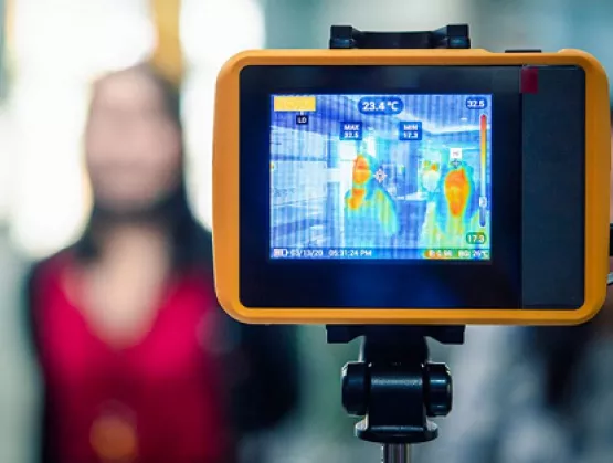
As government and business leaders start to talk about “returning to normal,” and looking to thermal cameras to help, questions remain about how and whether the latest technology can help prevent the spread of COVID-19.Across industries, everyone is looking for the right tools to help detect, slow and eventually stop SARS-CoV-2, the virus that causes COVID-19. By now we’ve all come to recognize that resuming operations in any way will require demonstrating measures to protect the health and wellbeing of people in a variety of situations, including travel and work.One proposed solution is thermal scanners. Unlike most medical imaging approaches, infrared (IR) thermography doesn’t require irradiation or expensive equipment, and presents no health hazard. Infrared radiation emitted from our skin can be detected and used along with information about the ambient environment to estimate core body temperature — which may indicate someone is running a fever, a common early symptom of COVID-19. While thermal cameras can’t detect a virus or a specific infection, they can help by quickly narrowing down a large pool of possibly infected individuals. And today, this represents the only viable non-contact mass screening approach for fever. The accuracy of the infrared system can, however, be affected by human, environmental and equipment variables. Understanding this multitude of variables — including the ways in which the science, technology and applications themselves interact — will help both users and system makers deliver the best results.Consideration #1: Think about the methodThermal detection has been used for fever detection for 20 years now. While older thermometers and thermal cameras, including the type used to detect a different coronavirus, severe acute respiratory syndrome (SARS), had their weaknesses, newer generations deliver significant performance improvements. More intelligent systems now offer features such as real-time calibration to ambient temperature with sub-degree °C accuracy, providing more accurate readings far more quickly than older generations.Newer camera systems are also more user-friendly and more reliable, featuring automated target recognition, improved resolution, pairing with a visible-light camera, automated alarms for febrile cases, and clearer outlining of hot spots. This higher degree of granularity improves insight, allowing for a more efficient and faster screening process, and provides on-site health professionals with necessary information to take additional steps when required. Advanced image processing features in new radiometric thermal cameras. Consideration #2: Know your baselinesBecause the environment can influence temperature measurements, some system makers have devised different ways to establish functional baselines. An early approach, recording a population baseline at each site on each day, proved too time- and resource-intensive. A newer approach, using a reference temperature source, or black body, offers evolutionary improvement. Designed to maintain itself at a specific temperature, the black body device allows the thermal camera system to automatically calibrate. Even better is a radiometric camera, which can intepret the intensity of an infrared signal reaching the camera. This requires more rigorous design and testing by the manufacturer, but it delivers much more precise measurements.Diagram of a fever detection system with black body emitter Consideration #3: Looking in the right place While thermal cameras can only detect surface temperatures, different parts of the human body more closely correlate with body temperature. Based on recent scientific research, the most reliable spot in the human face is the canthus, the small corners over the tear duct of your eye where the upper and lower eyelids meet. This kind of precise targeting requires accurate pixel calibration capabilities. The best surface target for estimating core body temperature: the canthus at the inner eye Consideration #4: Checking your performance Operating an IR fever screening system in the lab is one thing, but out in the field, the situation becomes more complex. Users need a camera system that is reliable and stable when it comes to critical performance factors like resolution, sensitivity and frame rate. Understanding the performance considerations when imaging a subject at a distance, for example, and realizing the minimum number of pixels required to get an accurate measurement are both essential in staging a fully optimal fever-detection platform.Consideration #5: Finding your way in the “wild west” of thermal imaging in early 2020People from the many industries that have been devastated by this pandemic – including travel, sports, manufacturing, food and hospitality, and entertainment — are looking for ways to reopen businesses safely while reducing the probability of a second wave of COVID-19. Deploying technology such as IR fever screening systems as part of a range of preventative measures will hopefully support that effort.As is the case with any promising emergent technology, there is a fair degree of chaos around the nuanced considerations of system design and performance. What standards apply to IR fever-screening devices? Which are being enforced? Who makes them? Will they work? IR camera manufacturers such as Teledyne DALSA and the expert system integrators we work with can play an important role in helping manufacturers and integrators to navigate this chaos, enabling us to work together to potentially save lives.For an even more in-depth look at this topic, visit this page, download our whitepaper Thermal Imaging Technology for Fever Screening, or browse.Jean Brunelle, product manager for infrared imaging, is a technical leader in sensor integration at Teledyne DALSA. He works on developing new image correction and calibration algorithms as well as qualification and production tests for the company’s visible and LWIR lines of digital cameras. Having earned a bachelor’s degree in engineering physics and a masters in surface chemistry, he has a passion for all things sensors, from how they work to how they are fabricated and used. His focus for the past few years has been on micro-bolometer-based LWIR cameras. Most recently, he was involved in the development and testing of Teledyne’s very own WLP micro bolometer and its integration into a thermal camera.Teledyne DALSA is a member of MEMS Sensors Industry Group (MSIG), a SEMI technology community that enables the MEMS and sensor industry to address common challenges, innovate and accelerate business results.
Read More
Since 2015, FlexTech has funded three projects with ITN Energy Systems, based in Littleton, Colorado. The projects all draw on a unique concept of using thin, flexible ceramic sheets as both a substrate for functional devices and as an integral part of the hermetic packaging to support paper-thin FHE products. Each program was increasingly sophisticated, enabling a larger variety of functions to be integrated into a common package. Independent functions such as energy storage, energy harvesting, or printed microelectronic circuits are deposited on their own ceramic substrate and the layers vertically stacked and interconnected into a monolithic structure that combines several functions in the smallest possible package volume.The ITN projects provide excellent examples of the power of collaborative research and development to help de-risk investments in next-generation electronics. All the projects were conducted with technical contributions from small and large businesses as well as university partners. The programs were funded by the U.S. Army Research Laboratories (ARL), directed by industry leaders and managed by SEMI FlexTech with the focus on utilizing the advantages of flexible hybrid and printed electronics (FHE) to create lighter-weight, lower-power, more conformable electronics than available commercially today. Markets ready to take advantage of FHE developments include healthcare, aerospace, mobility, consumer electronics, industrial electronics.ITN was founded in 1995 to focus on researching and developing technologies related to aerospace, energy and the environment for defense and commercial marketplaces. Its business model employs collaborative R D projects to explore, develop and validate promising next-generation clean energy technologies with an emphasis on tackling the manufacturing challenges that enable low-cost, high-volume production of thin-film devices on flexible substrates. Those technologies that meet the technical and business requirements of the market are commercialized via focused, spin-out companies with five such spin-outs formed so far. The work on ultra-thin batteries needed by the SEMI FlexTech community readily slid into their portfolio of projects.Project 1 – New Solid-State Lithium BatteryThe first project kicked off in 2016, with ENrG, and successfully supported the development and validation of novel Solid-State Lithium Battery (SSLB) products with total packaged thickness ranging from 50-250 microns. The SSLB proved to have substantial advantages in form factor and performance when compared with both commercial-off-the-shelf batteries and emerging technologies. For example, the SSLB provided more than double the operating time in a substantially smaller package in powering an audio device supplied by SEMI FlexTech partner companies.By avoiding the use of liquid electrolytes, the ITN SSLB also eliminates flammability issues while still allowing the benefits of lithium-based battery chemistry. The SSLB boasted many attributes attractive to the FlexTech community, including: Ultra-thin form factor, i.e. 250 microns thick, mAh class packaged batteries High volumetric energy density, i.e. baseline products with ~500 Wh/l and a roadmap to 1,000Wh/l The ability to support high current pulsing, i.e. current pulses at 4-10C rates, in support of demanding FHE duty cycles High temperature compatibility with solder reflow and other FHE integration schemes Rechargeability with high capacity retention at 1,000 cycles This new SSLB has formed the foundation of subsequent projects and commercialization efforts.Project 2 – Adding Energy Harvesting Based Recharging Capability The second SEMI FlexTech-funded project proposed a novel self-recharging battery with the addition of Lucintech’s cadmium telluride (CdTe) photovoltaics (PV), which was also deposited on thin yttria stabilized zirconia (YSZ) substrates. Because the CdTe supports a superstrate configuration, the SSLB can function as the back sheet for the PV package, thereby dramatically decreasing overall package thickness. The resulting flexible integrated power pack provided up to 0.25 Wh of energy storage and ~0.2 W of PV generating capacity in a total package less than 250 microns.As part of that effort, the ITN Team identified an effective power-management circuit that was ultimately compatible with die thinning and form factors very attractive to FHE. Consequently, the PV and SSLB were interconnected into a common power bus that enabled FHE to be operated with either the PV, SSLB or some combination of the two.ITN is seeing great interest in this product and both developing a version with substantially higher capacities than the project entertained for a UAV platform while ramping to low volume with support from NextFlex, a member of the Manufacturing USA network, and formed in 2015 through a cooperative agreement between the U.S. Department of Defense (DoD) and FlexTech Alliance.Monolithic integration of function layers atop of SSLB for high performance microelectronics device Project 3 – Integration with Processing and Sensor SystemsThe third FlexTech-funded project builds further on that foundation. In this project, the ITN Team is maturing the technologies to create a battery with an integrated processing and sensor system, nicknamed BiPASS. In addition to SSLB layers, the BiPASS package integrates printed circuits on YSZ employing high-performance, silicon- based bare die micro-electronics and/or thin film sensors into the common packaging. Mock-up of the charge control circuit on SSLB The initial demonstration integrates a commercial lithium battery charge control circuit within the SSLB packaging to create a monolithically integrated power module. There have also been promising developments of the University of Rhode Island’s metal oxide (MOx)-based thin film gas sensors that have dramatically increased sensitivity when deposited on thin YSZ. The resultant sensor achieves ppb detection of trace explosives gases that can be powered by SSLB. Along the way, ITN’s partners Molex and SunRay Scientific matured several aspects of FHE circuit printing and integration on both PET and YSZ, including new materials and processes for conductive traces, and bare die attachment with fine features. The project is in its final stages and the ITN Team now has a promising roadmap to integrate power, microelectronics, and thin film sensors/sensor systems into a single paper-thin package.Commercial Scale-Up StrategySince the initial demonstrations were completed, ITN has been actively maturing a commercial scale-up strategy based on significant market-pull and interest from several companies. A new venture to commercialize this next generation SSLB is in process. As part of those discussions, ITN is in active discussions with potential strategic partners to support the transition to high-volume production to access additional markets, many of which are cost-sensitive and need a higher degree of production maturity.In the meantime, ITN’s limited volume SSLB production line is already supporting medical device customers. In addition, a baseline SSLB (~2.5 mAh capacity) has been developed and tested in several new applications, including wearables, sensors and smart labels.“Based on the acceptance of these project in the market, I believe all three projects have provided significant value to the SEMI FlexTech community,” noted Brian Berland, Chief Technology Officer at ITN. “In addition, the connections and visibility we have gained within the industry by partnering with SEMI FlexTech have been invaluable. We are excited to continue this journey with new and additional projects. In the meantime, we are hopeful that our ongoing discussions with investment partners will support our commercializing of these components.”For more information visit www.flextech.org. SEMI FlexTech is currently (from 6/10/2020 – 7/17/2020) accepting white papers for new technology development projects. Read more at www.flextech.org.About the AuthorDr. Gity Samadi is the SEMI FlexTech Program Manager. Gity is responsible for the flexible hybrid electronics R D consortium activities including project awards and management, Technical Advisory Council management, and webinar/industry event planning for the building and fostering of this dynamic innovative community.
Read More
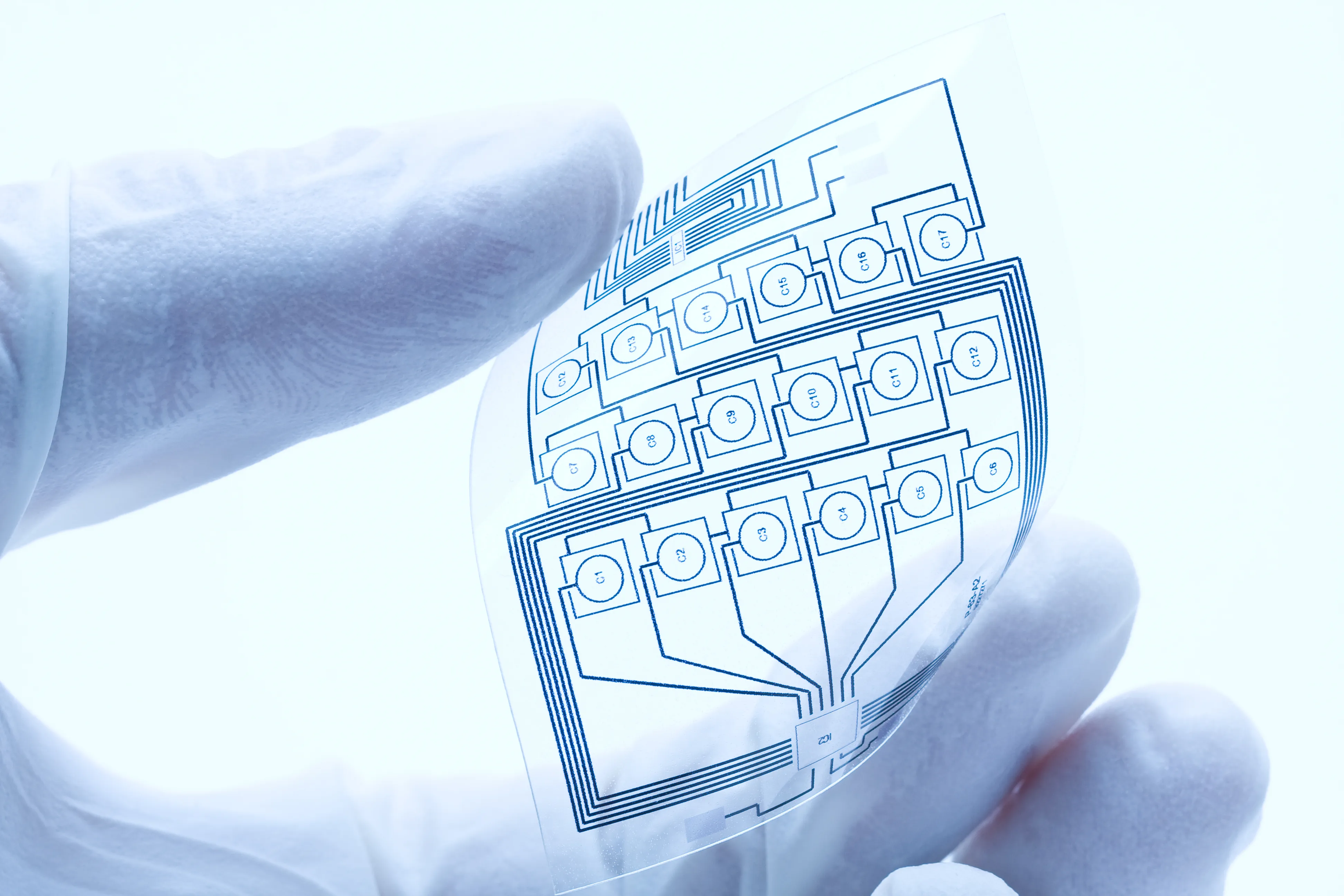
As the body’s largest organ, skin is responsible for the transduction of a vast amount of information. This conformable, stretchable, self-healable and biodegradable material simultaneously collects signals from external stimuli, which translates into information such as pressure, pain and temperature. The development of electronic materials, inspired by the complexity of this organ, offers a tremendous unrealized materials’ challenge. Fortunately, the advent of organic-based electronic materials may offer a solution to this longstanding problem.Zhenan Bao, K.K. Lee Professor of Chemical Engineering, Stanford University, is one of the world’s leading researchers working on the design of organic electronic materials that mimic skin functions. SEMI’s Maria Vetrano interviewed professor Bao to preview her February 25 keynote, Skin-Inspired Electronics, at FLEX|MEMS Sensors Technical Congress (MSTC) 2020, February 24-27, 2020, at the DoubleTree by Hilton in San Jose, California.Join us at FLEX|MSTC to meet Professor Bao and other industry influencers furthering innovation in flexible hybrid electronics (FHE) and MEMS sensors. Register now to connect with her at FLEX|MSTC or visit her on LinkedIn.SEMI: Your pioneering work on the use of electronic materials to construct second skin is a major step forward in human-machine interfaces. Could you please describe second skin?Bao: Second skin is a new electronic-device platform encompassing electronic devices that have skin-like properties such as stretchability, self‐healing ability, biocompatibility and biodegradability. In essence, the second skin is an electronic system of fully integrated multifunctional components operating on the surface of or inside the body to enable smart healthcare for disease prevention and treatment and to enhance the functional capabilities of natural skin. The second skin could also serve as a module to connect our human body to the Internet, thereby allowing human integration with the Internet of Things (IoT) for next‐generation wireless communications. In this way, we can view the second skin as an artificial body part that can be used to improve our everyday lives.SEMI: How might second skin operate in the human body?Bao: It has many potential uses. It could be a prosthesis for people who have lost their sense of touch. It could be used to repair damaged skin as well as to provide enhanced functionality that’s not possible with biological human skin. It could, for example, connect us with our external environment, with other people, even with our cars.I can also envision second skin as an implantable device for both neurostimulation and for early detection of disease. Schematic illustration of structure of second skin composed of functional devices: sensor, integrated circuit, display and power supply. Source: Stanford University SEMI: How did you get started in this research? Bao: Sixteen years ago when I started at Stanford, I learned of a colleague in mechanical engineering who was working on robotic cockroaches. That’s when I understood the need for sensor functions in robotics.I considered the large number of people with prosthetics who do not have a sense of touch. With this audience in mind, I started by designing a simple flexible electronic device that could take the shape of skin, even conforming to a robot hand, thereby approximating the natural sense of human touch.Once we developed the first sensor, and realized that its touch sensitivity could eclipse that of human touch, I asked myself: what can we learn from second skin – in addition to its sensing functionality?Skin is not just flexible; it is biodegradable and stretchable. So we started to dream. We began by developing electronic materials, either conductors or semiconductors. We added new functionality, such as self-healing properties, biodegradability and stretchability. That opened the way to new materials’ development.SEMI: What discoveries have you made in new materials?Bao: Over the past decade, we’ve developed skin-like materials with electronic properties that are on par with the best conducting and semiconducting polymers. Some of our skin-like semiconducting polymers can perform even better than amorphous silicon. That means with suitable processing methods, we can make stretchable ICs, initially with tens of transistors that can perform analog or digital functions, and in a later stage, stretchable displays driven by active matrix arrays.SEMI: What would it take to put these materials into production?Bao: We need to develop methods to pattern the skin-like electronic materials into fine features. We have been leveraging similar processes used for flexible circuit boards. Some research groups are developing roll-to-roll fabrication and printing methods.SEMI: Which technologies/applications are you commercializing?Bao: C3Nano is a Bao Research Group spin-off startup that is commercializing nanomaterials that are promising for bendable and foldable electronics.Another spin-off that is licensing our technology, PyrAmes, is developing a continuously non-invasive blood-pressure monitor. It’s not a cuff so the patient doesn’t have to remember to put it on.In the shorter term, we’re looking at putting artificial skin on prosthetic limbs and robotic hands. Further down the road, we could put skin on wounded regions of the body, forging connections to nerves that would support realistic sensation.To realize these applications, we’ll need to conduct further R D on materials and applications. The manufacturing of these devices still needs much more development.Fortunately, we’re part of a fertile development ecosystem at Stanford. I started the Stanford Wearable Electronics Initiative (eWEAR) to forge collaborations across Stanford campus as well as with industry.SEMI: What would you like FLEX|MSTC attendees to take away from your presentation?Bao: I’d like them to realize that the future of electronics is changing. I imagine a future in which the functions of a smartphone will disappear into what we wear, what we attach to our skin and what we implant inside our body. I believe that skin-like electronics will help to facilitate this future, allowing us to connect with each other and our surroundings in ways that feel natural, yet that also enhance our quality of life. Zhenan Bao is K.K. Lee Professor of Chemical Engineering with courtesy appointments in Chemistry and Material Science and Engineering at Stanford University. She founded the Stanford Wearable Electronics Initiate (eWEAR) and serves as the faculty director. Prior to joining Stanford in 2004, she was a Distinguished Member of Technical Staff at Bell Labs, Lucent Technologies from 1995 to 2004.Bao has over 500 refereed publications and over 65 U.S. patents with a Google Scholar H-Index 155. In her recent work, she has developed skin-inspired organic electronic materials, which have resulted in unprecedented performance or functions in medical devices, energy storage and environmental applications. She has pioneered several important design concepts for organic electronic materials. Her work has enabled flexible electronic circuits and displays.For more information on professor Bao’s research, visit Bao Research Group. FLEX|MSTC is organized MEMS Sensors Industry Group (MSIG) and FlexTech, SEMI technology communities focused on the growth of MEMS sensors and the flexible electronics supply chain, respectively. Maria Vetrano is a public relations consultant at SEMI.
Read More
A multidisciplinary team of researchers is developing new methods to collect and analyze sweat for clues about how the body is functioning.Imagine if you could know the status of any molecule in your body without needing to get your blood drawn. Science fiction? Almost – but researchers at the University of Arizona are working on ways to do this by measuring molecules in sweat.When physicians take blood samples from patients, they send the samples to labs to be analyzed for biomarkers. These biological clues indicate everything from cholesterol levels to disease risks, and they can be used to monitor patient health or make diagnostic decisions. The same biomarkers also are found in sweat.Using $519,000 in funding from SEMI-NBMC (Nano-Bio Materials Consortium), Erin Ratcliff, University of Arizona materials science and engineering professor and head of the UArizona Laboratory for Interface Science of Printable Electronic Materials, is leading a project to develop new ways of collecting and analyzing the clues sweat has to offer. Ultimately, this work could allow physicians to use patient sweat samples in the same way they currently use blood samples, for a less invasive and more informative approach to establishing and monitoring patient health.“What’s unique about this is that we are combining biology and engineering expertise to develop a wearable device that will detect molecules in sweat, so you don’t have to get your blood drawn to know the health status of your immune system, your nervous system, indeed, any system in the body,” said co-investigator and sweat biomarker pioneer, Esther Sternberg, MD. “The goal, eventually, is to create a device that will provide physicians and health care providers the ability to monitor your health status continuously and in real-time without needing to draw blood.” Materials science and engineering professor Dr. Erin Ratcliff in her laboratory at the BIO5 Institute at the University of Arizona “We are pleased to sponsor and eager to complete this project with University of Arizona’s impressive team bridging the disciplines of engineering and life sciences,” notes Melissa Grupen-Shemansky, PhD, Chief Technology Officer and Executive Director of SEMI-NBMC. “A concerted interdisciplinary approach at the early stages of R D is relatively new and there is much learning on both sides. The UA team brings unique strengths in both areas and we are excited to be partnering and collaborating with them.”Ratcliff’s co-investigators are J. Ray Runyon, a research assistant professor in the Department of Environmental Science, and Sternberg, research director for the Andrew Weil Center for Integrative Medicine; director of the Institute on Place, Wellbeing, and Performance; and the Andrew Weil Inaugural Chair for Research in Integrative Medicine. Ratcliff and Sternberg are both members of the BIO5 Institute.Standardized Sample CollectionIn order to study sweat, researchers need to collect samples of it, and there are a number of ways to do so.“The obvious idea would be to make a patch that gets information from many pores at once, but the problem is that this creates a space between the patch and your skin, and you have to wait for it to fill up with sweat,” Ratcliff said. “We hypothesize that while you’re waiting, these molecules – the very molecules you’re trying to detect and analyze – are changing chemically.”The team’s first task is to develop new, continuous and hands-free collection devices that deliver high-quality, standardized sweat samples. This will allow health care professionals to gain a more holistic picture of a patient's bodily systems over an extended period, rather than the “snapshot” a blood draw can provide of a particular moment.Currently, sweat labs across the world are using different methods to collect samples, which limits researchers’ ability to compare data. Standardizing the collection method could provide researchers, including medical device developers, with a new degree of confidence in sweat sample data.“High-quality data, with respect to different target molecular biomarkers in sweat, requires that a high-quality sample be collected,” Runyon said. “This will be the first hands-free method that will truly take into account the interplay of the chemistry of sweat, the target biomarker and the device material.” University of Arizona student in classroom testing medtech devices Low-Level DetectionThe team is also developing methods for researchers to detect and analyze neuropeptides in the collected samples. Used by neurons to communicate with each other, these small molecules are involved in biological functions, including metabolism, reproduction and memory. Commercial wearable devices monitor metrics like heart rate, and some use sweat sensors to monitor dehydration level. Measuring neuropeptides, however, will allow researchers to zoom in millions of times closer to investigate stress and relaxation responses at the molecular level.“The idea is that your sweat is reflecting your nervous system – all of the neurotransmitters your body uses to signal between the brain and the rest of the body,” Ratcliff said. “Monitoring this biochemical response continually, over a 24-hour cycle, can inform us about the health of the wearer and also act as a diagnostic tool.”Meet Dr. Ratcliff and the University of Arizona team at FLEX in San Jose, Calif., February 23-26, 2020. Emily Dieckman is Editor at The University of Arizona. Republished with permission from the University of Arizona.
Read More
MEMS technology has changed human interaction with electronic devices. Introduced in the 1990s, the first mass-market MEMS devices were used for inkjet printheads and automotive airbag crash sensors. Today, MEMS are ubiquitous, with billions of the tiny devices adding intelligence and interactivity to smartphones, smart speakers, wearables, automobiles, biomedical devices, remote monitoring and event detection systems, and countless other applications. Integrating MEMS with Flexible Hybrid Electronics (FHE) is an important step in the evolution of this miniaturized intelligent sensing technology, paving the way for its use in new classes of flexible, conformal devices.The integration of the two technologies promises to breed new applications in small form factors but also presents challenges inherent to FHE design and fabrication processes. SEMI’s Nishita Rao caught up with Nathan Pretorius, prototyping and automation engineer, NextFlex, to discuss MEMS-FHE device integration challenges and opportunities ahead of his February 26 presentation, Integrating MEMS Devices in FHE, at FLEX|MEMS Sensors Technical Congress (MSTC) 2020, February 24-27, 2020, at the DoubleTree by Hilton in San Jose, California.Join us at FLEX|MSTC to meet Nathan and other industry influencers advancing innovation in FHE and MEMS sensors. Register now to connect with him at FLEX|MSTC or visit him on LinkedIn.SEMI: Why is integrating MEMS devices into FHE systems important? What new use cases might it enable?Pretorius: The main value proposition of integrating MEMS devices into FHE is that it allows MEMS devices to exist in a different form factor than was possible previously, giving us high-quality MEMS sensors on the flexible and conformable platform of FHE.Ease of application, flexibility, lower cost and rapid iteration on a design are just some of the benefits of FHE devices. And because there are few robust FHE sensors that overlap with MEMS’ capabilities, when you combine the two, you get a lot of compelling uses. That’s why NextFlex is working with agencies and companies to evaluate MEMS’ integration, including using bare MEMS die with microfluidics and promoting new ways of attaching and packaging MEMS die for use with FHE. SEMI: Why is FHE an ideal platform for integrating various types of sensors?Pretorius: MEMS integrated with FHE devices are ideal for rapid design and deployment of data-gathering sensor nodes — which we can iterate for specific applications. A few examples include on-body health monitoring devices for bio-fluids analysis, medical pressure sensors for monitoring blood pressure, and peel-and-stick sensors nodes for infrastructure monitoring. In terms of design and production, FHE devices support rapid prototyping, allowing for instantaneous design-iteration cycles. This speeds design-to-production over traditional rigid PCBs and copper flex because the feedback cycle time between design, manufacturing and testing is shorter, accelerating time to market. What’s exciting about FHE technology is that a variety of sensors or components, including MEMS, can be designed into the base system to easily customize it for a specific application. In addition, our experience shows that when compared to a traditional rigid PCB, an FHE board reduces manufacturing steps and device weight by two-thirds and, perhaps most importantly, converts the device to a thin, conformal shape that makes possible products in new form factors. SEMI: What are the primary challenges to integrating MEMS with FHE? What is NextFlex doing to help device manufacturers address these challenges? Pretorius: There are a few challenges, some of which are device-specific. Most recently, I’ve been focusing on inertial and timing devices, including accelerometers, gyroscopes and resonators. There are a few technical challenges involved in the process of getting the devices from the wafer to an FHE substrate. The wafer processing is very important, especially the dicing and thinning steps. After thinning and dicing, the die is placed onto the FHE substrate. The stresses caused by bonding to the substrate have to be understood and characterized. After placing the die, you then have a calibration step, which is normally performed after the device is packaged. With a MEMS die placed onto directly onto an FHE substrate, calibration then must be done.Finally, the device encapsulation is important, since on an FHE substrate the hard-to-soft material transition is very important to mitigate stresses to rigid component interfaces. We have also been looking at how to work with devices that have damping vents. Flexible encapsulants are inherently more permeable to gases and water vapor than hard encapsulants, so studying the encapsulation of MEMS devices on FHE is another area of interest. NextFlex has been working in a supporting role to evaluate best design practices and best attach and integration methods. In addition to our ongoing collaborative programs, NextFlex is developing the FHE manufacturing ecosystem to include system and component manufacturers and designers, product developers, and materials and equipment providers.SEMI: How do we facilitate closer collaboration between the FHE manufacturing ecosystem and MEMS suppliers such as MEMS device manufacturers, product developers, and materials and equipment providers?Pretorius: It’s important to include manufacturers early in the design process so we can identify challenges up front. That’s why NextFlex spearheads technology road-mapping efforts that include representatives from across the manufacturing ecosystem. We use the roadmaps to prioritize challenges that we can address effectively through collaboration, focusing the industry on solving problems through Project Calls that reveal integration challenges and results from real devices and that tell us how the materials and equipment actually perform with a real device.NextFlex keeps the information flowing, holding quarterly project update webinars to share results. As current devices are optimized for the process in which they will be used, we learn a lot from the project performers who make FHE system demonstrators — and we share that information with the member community. SEMI: Can you point to an example of a successful MEMS-FHE device integration?Pretorius: MEMS-FHE integration is still in the early stages, but we are working on several projects including a DARPA Seedling project for which we have integrated MEMS sensors into FHE systems for testing and evaluation. We plan to continue this work by integrating MEMS and FHE devices using methods that support mass production.SEMI: What would you like FLEX|MSTC attendees to take away from your presentation?Pretorius: We would like to see the FHE community work more closely with MEMS device manufacturers. For example, NextFlex often works with manufacturers to gain access to bare die, which is still a significant hurdle in making devices.The best way to speed things along is to get involved. We encourage FLEX|MSTC attendees to join NextFlex. As a prototyping and automation engineer at NextFlex, Nathan Pretorius explores new print methods for prototyping and automation using novel materials and processes. Pretorius currently focuses on how best to apply software scripting and machine learning to streamline FHE processes. Prior to joining NextFlex, he researched the strengths of roll to roll and screen printing on printed electronics designs, including capacitive touch interfaces, FHE passive component design, and antennas. Nathan holds a Bachelor of Science degree in Graphic Communications from Clemson University. FLEX|MSTC is organized MEMS Sensors Industry Group (MSIG) and FlexTech, SEMI technology communities focused on the growth of MEMS sensors and the flexible electronics supply chain, respectively.Nishita Rao is marketing manager for technology communities at SEMI.
Read More
VTT Technical Research Centre of Finland Ltd (VTT) has its sights set high. As a leading global research and development firm , VTT is out to produce bio-interfacing and biodegradable flexible hybrid electronics (FHE) devices that help tackle some of the world’s greatest challenges including environmental degradation and food scarcity.SEMI’s Maria Vetrano interviewed Antti Vasara, president and CEO of VTT Technical Research Centre of Finland, to preview his February 25 keynote, Beyond Flexible Hybrid Electronics: Biodegradable Electronics and Interfacing Bio+Electronics, at FLEX|MEMS Sensors Technical Congress (MSTC) 2020, February 24-27 at the DoubleTree by Hilton in San Jose, California. Join us at FLEX|MSTC to meet Antti and other industry influencers driving innovation in flexible hybrid electronics (FHE) and MEMS sensors. Register now to connect with him at FLEX|MSTC or visit him on LinkedIn.SEMI: What is body-interfacing electronics and what is your vision for bio-interfacing and biodegradable electronics?Vasara: Body-interfacing electronics have existed for decades. Developed in the 1970s, the wireless heart rate monitor is a good example. While continuous heart monitoring with a compact, inexpensive wearable device is widely accessible technology, other bodily parameters, such as cholesterol levels or biomarkers, are diagnosed every time we see a doctor. Establishing a baseline using multiple measurements — before symptoms develop is actually much more effective.That’s where bio-interfacing comes in. Bio-interfacing devices will continuously measure and analyze complex biogenic substances such as sweat, breath, blood and urine. A smart patch for continuous sweat monitoring, for example, would overcome several challenges: supporting electronics functionality in liquid environments, managing the transport of harvested samples to and from the sensor, managing potential contamination, and disposing of samples after measurement.While FHE in principle delivers the right building blocks and is an ideal form factor for a wearable sweat analytics patch, flexible circuits are not ready for out-of-the box interaction with biological matrices. Hence, our mission at VTT is to anticipate and develop the upscaling process know-how required for FHE devices that either interface with biological systems — or that must themselves biodegrade.We’re also focusing on biodegradable electronics because environmentally conscious end-users and manufacturing companies want biodegradable versions of energy-autonomous, label- or sticker-like Internet of Things (IoT) sensors. Typically used for packaging, logistics, environmental monitoring and medical diagnostics applications, these sensors — which have a lifetime of a few days, weeks or months — have become very popular. Unless they are biodegradable, however, they just add to landfill.SEMI: What approaches is VTT using to develop bio-interfacing and biodegradable electronics?Vasara: In our Business Finland-funded ECOtronics project, we are working with our partners to create recyclable and compostable electronics and optics that use renewable resources. For example, devices developed using substrate materials like paper, cardboard or VTT’s in-house-developed nanocellulose films and biopolymer films for environmental monitoring or skin patches can be easily recycled or even biodegrade naturally. Where possible, we use roll-to-roll printing to generate the device circuitry, and on a component level, we have optimized our assembly process towards bare-die component bonding to reduce the overall footprint of non-biodegradable waste per device.SEMI: What use cases do you find most promising and why?Vasara: A prominent example of a single-use test that generates a large amount of waste is the digital pregnancy test. When breaking it down into components, you will find a rigid circuit board with microprocessor, a couple of coin cell batteries, a liquid crystal display, a LED light source and photodiode, and a large chunk of plastic packaging around it. The materials and battery capacity of such a device would be sufficient to run hundreds of pregnancy tests – actually technical overkill.By using printed circuits on biodegradable substrates, bare-die assembled components (ASIC, LED light sources, photo diodes, thin film batteries as power sources) and device packaging composed of biodegradable plastics, we can completely redefine the environmental footprint of single-use tests. We are currently developing a toolbox for our customers to turn their existing conventional test into an ecotronic form factor.Another exciting use case is a sweat sensor that we developed collaboratively with Ali Javey, Ph.D., professor of Electrical Engineering and Computer Sciences, UC Berkeley, and the co-director of Berkeley Sensor and Actuator Center (BSAC). Together with his team, we created a wearable electrochemical sensor for continuous sweat analysis during exercise. With the UC Berkeley group providing the chemistry to monitor N+, K+ ion and hydration levels in sweat over the duration of several hours, VTT delivered the underlying sensor platform, featuring the printed sensor electrodes and sweat harvesting microfluidic channels for fluid management and transport. It’s exciting to see what we can achieve by combining techniques from different disciplines, in this case electrochemistry, printing, packaging and microelectronics.SEMI: How can industry enable the development/manufacture of flexible FHE devices? Where does VTT fit into the ecosystem?Vasara: As many FHE devices target large-volume markets, scalability of manufacturing is key: How can I get from one device (= working prototype) to a handful of devices (= feasibility study), to thousands (= pilot manufacturing), to a million (= mass manufacturing) without compromising the quality of the system’s performance and reliability?Access to upscaling infrastructure is essential for the development of novel FHE devices and methods, but infrastructure is expensive. That’s where our establishment of a roll-to-roll pilot printing line to bridge the gap between laboratory R D and mass manufacturing has proved invaluable. We can provide a unique worldwide upscaling infrastructure for advanced FHE devices, with a strong focus on large-area roll-to-roll processes and hybrid assembly. This service removes our customers’ burden of high infrastructure investment in early development stages and it allows us to guide customers along their development path, from prototype to mass production.Watch our video: VTT pilot manufacturing for diagnostics and wearablesSEMI: Is there anything else that device manufacturers need to know in order to succeed?Vasara: In my eyes, the success of FHE devices eventually depends on several factors: It requires a high degree of automation, well-optimized processes, reliable supply chains, and perhaps most importantly, clear standards and rules for designers to guarantee flawless interoperability of all the different elements on a flexible and hybrid circuit. Let us not forget – we are trying to marry electronics with printing, biology, packaging, microfluidics, injection molding and other fields of expertise.We recently finalized the compilation of a set of design rules for publication in our state-of-the-art overview of printed and hybrid electronics manufacturing methods. You can download the overview, PrintoCent Handbook, for free.SEMI: What would you like FLEX|MSTC attendees to take away from your presentation?Vasara: The latest technologies and innovations in microelectronics, MEMS, printing, materials, and biosensors provide us a toolbox for true innovation in the FHE space. Now we need cross-disciplinary thinking and daring steps to combine different manufacturing methods and skill-sets. The ideal cross-disciplinary team might include: The printing engineer who knows how to design contact pads for a bare-die IC assembly The biologist who knows about the thermal and mechanical stress in a printing environment to design processes for bio-functionalization of surfaces The electronics engineer who knows how to optimize a circuit powered with an enzymatic biofuel cell The number of sensors deployed on (or inside) our body, in our drinking water, in our cars, on our fields, in our pets, and everyday products will surely grow. Let us make sure they leave the smallest environmental footprint possible.Antti Vasara, Ph.D. has been the president and CEO of VTT Ltd since 2015. VTT is a visionary research, development and innovation partner with over 2000 people and a turnover exceeding 250M EURO. Vasara is president of EARTO (European Association of Research and Technology Organisations) and is chairman of the board of Palta (Finnish Service Sector Employers). In addition, he is a non-executive director of Elisa Oyj (largest communications operator in Finland) and a board member at EK (Finnish Confederation of Industries).He has served on several high-profile groups on industrial and innovation policy of the European Commission, in addition to several groups in Finland on artificial intelligence and research policy. Previously, Vasara spent close to 25 years in private industry, working at Nokia, Tieto, SmartTrust and McKinsey Company. Earlier in his career, he was a researcher in optical communications with 20+ peer-reviewed articles and one international patent. Vasara holds a Doctor of Science (Technology) degree from Aalto University in Finland.For more information about VTT’s work in bio-interfacing and biodegradable FHE devices, visit VTT Research. FLEX|MSTC is organized MEMS Sensors Industry Group (MSIG) and FlexTech, SEMI technology communities focused on the growth of MEMS sensors and the flexible electronics supply chain, respectively.Maria Vetrano is a public relations consultant at SEMI.
Read More
Today’s mobile devices are smaller, more power-efficient, and have more capability than we could have imagined just a decade ago. Offering ever-increasing levels of user functionality, mobile devices are now ubiquitous, and are rapidly becoming the primary mechanisms through which we interact with the digital world, our physical environment, and one another. An unintended side effect of our dependence on the current crop of mobile devices is that they are driving us to distraction.A major industry dynamic will shake things up for the better. Sensors are getting smaller and more efficient, and they’re offering attractive new functionality, giving us the ability to monitor our air and water quality, assess potential toxins in our food sources, and analyze personal health conditions, to name a few use cases. At the same time, the realization of flexible hybrid electronics (FHE) through new materials and production processes, better integration with other electronic components, more efficient energy production and consumption, and pervasive wireless connectivity are fueling the next generation of devices and experiences. What can we expect from tomorrow’s mobile devices — and how can we manage them, instead of having them manage us?SEMI’s Nishita Rao caught up with Mike Wiemer, Ph.D., VP of Engineering, CTO and co-founder, Mojo Vision, to preview his February 25 keynote, The Art of the Possible, at FLEX|MEMS Sensors Technical Congress (MSTC) 2020, February 24-27 at the DoubleTree by Hilton in San Jose, California.Join us at FLEX|MSTC to meet Mike and other industry influencers advancing innovation in FHE and MEMS sensors. Register now to connect with him at FLEX|MSTC or visit him on LinkedIn.SEMI: Mojo Vision has conducted its own research on human interaction with mobile devices. Why is this important?Wiemer: Our mobile devices have given us access to the information we need and want, improving many aspects of our lives. But our devices have also influenced our relationships and attention to our environment in negative ways. We believe that the next mobile computing platform must improve this situation. Instead of pulling us away from the moment, our devices need to embrace more human-centric engagement while still letting us access information that improves our quality of life. Mojo Vision has worked to understand this problem through our own studies and research so we can better develop an approach to address it. SEMI: How are key technical trends driving size, efficiency and capability advancements in mobile devices?Wiemer: Tiny low-power sensors are enabling ever-smaller feature-rich mobile devices that run longer on a battery charge. Smartwatches are a good example. Just a few years ago, smartwatches were not that much more than small screens on our wrists. Today, we have GPS, EKG/health monitoring, and cellular wireless interfaces all inside the same form factor.As this trend continues, we at Mojo Vision predict that our devices will continue to shrink and become even more personal: They’ll be more continuously worn and matched to our own needs and behaviors. This trend towards invisible personal devices is something we’re trying to accomplish with our solutions at Mojo Vision.SEMI: What is Mojo Vision’s concept of “Invisible Computing?” Wiemer: Our vision of Invisible Computing is based on the idea that our wearable devices should be invisible to those around us, encouraging more human interactions. These wearables should be invisible and unobtrusive to users themselves. Our Mojo Lens, which contains a full display and sensors housed inside a contact lens platform, exemplifies this vision. Using proprietary microelectronics and the world’s densest microdisplay to layer digital images and information seamlessly, Mojo Lens is redefining augmented reality. Our mobile devices today continue to increase the quantity and magnitude of interruptions. We think that shouldn’t happen. As a socially invisible device that delivers contextual, relevant content, the Mojo Lens lets us go about our daily lives, naturally interacting with other people while simultaneously enjoying the benefits of augmented reality. We think Invisible Computing can change our relationship with our devices, as well as seemingly give us superpowers. For more information, download the Mojo Vision report, Device Distraction: Understanding the Problem, Re-Thinking the Solution.SEMI: Can you tell us more about Mojo Lens?Wiemer: At its foundation, Mojo Lens is a nanoLED display, radio and sensor platform, integrated using flex technologies, and placed on your eye to provide important information. Mojo Lens can elevate or suppress this information to decrease reliance on your other devices.Unlike your smartwatch or smartphone, which react to you in a binary manner because they don’t have enough information to make autonomous decisions, Mojo Lens understands the context of your experience. That’s because it’s based on our Invisible Computing platform, which can understand your activity. Mojo Lens recognizes if you’re engaged in a conversation, driving or having a coffee, and it reacts with information accordingly.Mojo Lens could act like a real-time interpreter, for example. When someone speaks to me in a language I don’t understand, I should see “subtitles.” Or if I’m having a conversation with someone, Mojo Lens wouldn’t interrupt me with a notification at that moment. For the 92% of Americans who are interrupted by their devices during conversations every day, this prioritization can boost productivity. More importantly, it can improve the quality of our connections with the people around us.Mojo Vision’s microLED platform offers a world-record pixel pitch of over 14,000ppi and pixel density of over 200Mppi², making it the smallest, densest display for dynamic — or moving — content. SEMI: What would you like FLEX|MSTC attendees to take away from your presentation?Wiemer: It feels like the speed at which people are defining important problems and tackling them is increasing every year. And there are so many important problems to solve: space travel, autonomous driving, electric vehicles, alternative energy, quantum computing, lifespan extension, increased food production, brain-computer interfaces, AR/VR. All these problems seem impossible and “crazy,” until some group of people comes along to put a framework in place that can address them. Interestingly, these frameworks aren’t necessarily new. Rather, they build upon existing technologies and capabilities.MEMS sensors and FHE are good examples. From smart textiles, flexible displays and biological sensors to miniature radars, MEMS sensors and FHE technologies are essential building blocks. Many of the big problems we can imagine today will be solved by stacking today’s MEMs and FHE technologies in imaginative new ways. So what do we do next? I’d like to encourage FLEX|MSTC attendees to first define the problem to solve and then define the technology — rather than starting with the technology solution. Mike Weimer is a serial entrepreneur and proven science and technology leader in complex systems development and integration. Before co-founding Mojo Vision as CTO, Weimer co-founded and served as president at Solar Junction, a high-efficiency solar cell company (acquired) where he and his team set two world records for the highest-efficiency solar cells ever made by humans.After Solar Junction, Wiemer joined New Enterprise Associates (NEA) as an Entrepreneur in Residence where he sourced new investments and helped portfolio companies to develop their business and funding strategies. He is a board director at Stratio Corporation and an advisor at Stanford’s StartX Accelerator. He holds a B.S., M.S., and Ph.D. in Electrical Engineering from Stanford University.For more information, visit Mojo Vision.Interested in engaging with the MEMS sensors supply chain? MEMS Sensors Industry Group is a SEMI technology community that enables professionals in the MEMS and sensors industry to accelerate business results by addressing common challenges and opportunities.Nishita Rao is marketing manager for technology communities at SEMI.
Read More