downloadGroupGroupnoun_press release_995423_000000 copyGroupnoun_Feed_96767_000000Group 19noun_pictures_1817522_000000Member company iconResource item iconStore item iconGroup 19Group 19noun_Photo_2085192_000000 Copynoun_presentation_2096081_000000Group 19Group Copy 7noun_webinar_692730_000000Path
Skip to main content
Default Banner Image

IoT

Digitimes Research is predicting a doubling of the global SOI market between 2019 and 2024, "...thanks to significant expansion in applications to mobile devices, communication infrastructure, IoT devices and automotive electronics in the 5G era...". (Read the full article in Digitimes here.) Beyond the continued enormous success of SOI in front-end modules (FEMs) for RF (aka RF-SOI, which as we know is found in every smartphone on the planet), the report cites high growth specialty areas such as imaging chips for smartphones and photonics in data centers. They also predict that FD-SOI will be "massively applied" in 5G, with applications in base stations and data centers. And of course, low voltage and low power consumption will be the big drivers in IoT and wearables. All this is driving Soitec, the major SOI wafer manufacturer, to expand capacity at its facilities in France and Singapore in 2020, says the report. This is happening in strategic cooperation with Shanghai-based Simgui. As noted in ASN about a year ago, Soitec and China’s SOI wafer leader Simgui announced an enhanced partnership and increased production capacity of 200mm SOI wafers in China, securing future growth. At that time the two companies redefined their manufacturing and licensing relationship to better serve the growing global market for RF-SOI in mobile and Power-SOI in automotive and consumer electronics. Separately, Okmetic of Finland, which specializes in SOI wafers for MEMS, sensors and RF, is also doubling its capacity (we covered their 2019 Shanghai presentation here.) (Image courtesy: Soitec)
Read More
Here is our second post about the SOI Consortium’s Japan Symposium this past fall. This will provide summaries of eight very informative presentations on SOI in IoT and automotive by NXP, Dolphin Design, Leti, Silvaco, Arm, I-fuse and Secure-IC. There’s a lot of content to summarize, so this post is about twice as long as those we usually do. But you’ll want to read right to the end, for sure! In case you missed our previous post on the 5G/RF-SOI presentations given at the Japan event, you can read it here. Our next and final post on the Japan event will cover photonics presentations by Cisco/Luxtera, TowerJazz, GlobalFoundries, Leti, Cadence and Soitec. By way of reminder, the Japan SOI Symposium was a great success, with both days well attended. If your company is a member of the SOI Consortium, you can now access most of these presentations on our website. You can also click on the illustrations in this post to see them in enlarged versions. [caption id="attachment_28106" align="alignleft" width="366"] (Courtesy: NXP SOI Consortium)[/caption] The IoT World Enabled Through SOI - Jon Cheek, NXP Sr. Director, Front-End Innovation For NXP, FD-SOI introduced the ability to easily add different functionalities to the technology node like ULP, eNVM, support for high-voltage and embedding RF. For them, said Cheek, it’s about the range, and with adaptive back bias, you can “get crazy”, so you can really achieve amazing things. In fact, they think they now have the lowest leakage SRAM in the industry, thanks to body biasing. The i.MX 7ULP is finding significant success in wearables. Their “crossover” chips are the latest beneficiaries of FD-SOI with body biasing. The “new normal”, they offer huge improvements for real-time operating systems – which is of course key for edge computing. (As you can imagine, the audience was intently taking notes throughout -- this was a really excellent talk!) It also is great for machine learning, as it is designed to unlock the potential of voice-assisted end nodes. The IP they needed is now available from multiple vendors, noted Cheek, such as Tensilica and VeriSilicon. Another key play will be in visuals for industrial computing. He concluded by observing that the automobile is the ultimate IoT machine, with 10x the amount of code now found in leading edge airplanes. That’s where the i.MX8 and 8X come in. [caption id="attachment_28104" align="alignright" width="323"] (Courtesy: NXP SOI Consortium)[/caption] High-Voltage SOI – Enabling Automotive- NXP Jon Cheek gave this presentation on the second day of the Japan event. Long-time followers of SOI will know that NXP has been excelling in high-voltage (HV) SOI for well over two decades now (including the pioneering work done by Philips, now part of NXP: their EZ-HV SOI patent dates back to 1993). It’s probably safe to say that NXP's SOI-based automotive chips are used by virtually every carmaker on the planet. HV follows well behind the leading edge – it’s currently mostly around 130nm (the limits are related to metalization). Reason #1 it’s on SOI? SOI-based technologies are incredibly reliable, especially in the automotive culture targeting the three zeros (0 emissions, 0 accidents and 0 time wasted). Today’s car manufacturer’s are going to a distributed environment, and SOI still provides a huge advantage, making parts that are smaller, lower power and more reliable – so it drives a lower BOM for automakers.In conclusion, said Cheek, NXP’s leadership through SOI innovation enables scalable solutions, high voltage analog integration, sensor integration, and reliable safe passenger experience. [caption id="attachment_28101" align="alignleft" width="432"] (Courtesy: Dolphin Design SOI Consortium)[/caption] Improving SoC Energy-Efficiency with Dolphin Design Platforms – Nicolaus Gaude, BizDev Product Marketing, Dolphin Design Dolphin has a series of platforms, techniques and IP for increasing speed and drastically improving energy efficiency in SoC design. Gaude introduced their Speed Platforms, which include a Power Management Platform and a Processing platform, both of which make dramatic improvements in energy efficiency. The Power Management Platform keeps control of power management from architecture to design, resulting in a 10x improvement in energy efficiency. The Processing Platform comprises configurable RTL clusters for best-in-class (100x) energy-efficiency. Gaude then turned to the Dolphin’s Adaptive-Body Bias (ABB) IP for breakthrough energy-efficiency with FD-SOI. This is real-time, “on-the-fly” body biasing: the IP does it all. It is silicon-proven on GlobalFoundries’ 22FDX with Arm cores and Invecus standards cells SRAM, with breakthrough energy efficiency. [caption id="attachment_28108" align="alignright" width="363"] (Courtesy: Silvaco SOI Consortium)[/caption] Platform Infrastructure for SOI-IP Ecosystem – Thomas Blaesi, VP of Global Marketing, Silvaco The massive use of IP is both an advantage and a challenge, began Blaesi. There are solutions out there, but they are disconnected. Typically SoC/IP designers, IP librarians and support folks use various systems, while procurement, finance and legal use others. This is a problem for both the providers and the consumers of IP. Silvaco has a new system called Xena that centrally organizes all IP data: it’s an IP repository for tracking accounts, products, contracts, devices, support, compliance and reporting. One of the first beneficiaries of Xena will be the SOI ecosystem, as providers of SOI IP are already signing on. Beyond the organizational advantages, Xena has patented “finger printing” and “DNA analysis”, so there is a digital representation of each IP on an SoC that can’t be reverse engineered. Each fingerprint contains list of unique signatures of each file in an IP or SoC. A file’s unique signature is created from the entire file content, and that signature is guaranteed to be unique to that content. It enhances support for all versions of common design files: hard IP, soft IP, and embedded software. Because it’s cloud or enterprise based, it will be particularly useful for large organizations. Fingerprinting and DNA analysis are vendor agnostic, universal, and easy-to-use tools and methodologies for IP lifecycle management, he concluded. [caption id="attachment_28103" align="alignleft" width="463"] (Courtesy: Leti SOI Consortium)[/caption] Ultra-low power, FD-SOI based IP, in the space of IoT, Health Care, Smart Connectivity 5G – Michael Tchagaspanian, EVP Industrial Partnerships, CEA-Leti This presentation began with a review of the explosion in devices with IoT and related investments, then connected all the ways in which innovations powerhouse Leti is contributing – from the SOI wafer level to the chip level – which is to say practically everywhere! Especially hot topics in FD-SOI included: the roadmap to sub-10nm; CoolCube monolithic 3D; new embedded memories; power amplifiers; Ultra-Wide Range DSP; smart sensing local processing (including haptics, imaging, infrared advanced processing); local processing with edge AI; and spike coding for deep neural networks. He showed information on two always-on/on-demand transmission 28nm FD-SOI IoT test chips that taped out in mid-2019: the Warrior and the Samurai. And finally, he covered silicon-proven IP that Leti has for FD-SOI including power management blocks, lots of RF IP (including low-power RF wake-up), sensor interfaces, clockless network-on-chip and new SRAM technologies. These and more will be covered at the next Leti Innovation Days in Grenoble (June 2020) – during which in parallel, btw, there will also be a European SOI Summit hosted by the SOI Consortium. [caption id="attachment_28099" align="alignright" width="475"] (Courtesy: Arm SOI Consortium)[/caption] FDSOI Enablement for a Total Compute Future – Manuj Rahor, Director Emerging Technologies Product Marketing, Arm Subtitled A perspective on system optimization with Arm FDSOI IP, this presentation reviewed how Arm is enabling system gains through optimization across IP boundaries. This is work happening in the Arm Artisan Physical Design Group (PDG), which provides logic, memory and POP (processor optimization package) IP as well as various products to help ease implementation challenges for advanced nodes. In this case the focus is on Total Compute enablers on Samsung 28nm FD-SOI (called 28FDS) – specifically three building blocks recently launched on FD-SOI. The first is the 128Mb Wide Capacity embedded MRAM (an eNVM to replace eFlash) compiler for storage delivered to Samsung in July `19. It was demonstrated in silicon in the Musca-S1 Smart IoT Device Demonstrator on 28FDS, an energy efficient IoT device with eMRAM secure boot on-chip storage. [Read our coverage from March 2019 here.] The second is a novel design developed with Spin Memory. It recently taped out on 28FDS and is slated for delivery in 2020. Adding an “Endurance Engine to the eMRAM that was delivered in 2019, the ARM-Spin innovation delivers RAM-like performance with increased speed and endurance. What’s at issue here is a change in use cases. Use cases served by eFlash were not written to that often; now with sensors (as in IoT) that continually gather and write data, eFlash endurance is not sufficient. The third is billed as an SRAM replacement compiler. Its MRAM as RAM in A-class systems, with significant energy and performance gains. Again, this is a use-case issue: retention is lower (this is for weeks months, whereas the other solutions are for 10 years). But you can get more RAM than SRAM into the same footprint, so you get a 60% reduction in DRAM traffic and increased performance. Delivery for this is marked as 2020+. [caption id="attachment_28100" align="alignleft" width="294"] (Courtesy: Attopsemi SOI Consortium)[/caption] I-fuse™: A Disruptive OTP Technology – Dr. Shine Chung, Chairman, Attopsemi I-fuse is a disruptive OTP (One-Time Programmable) technology without disrupting a fuse. The goal was a 100x increase in reliability at 1/100th of the cell size and 1/10th the power. It has now been demonstrated in GlobalFoundries’ 22FDX FD-SOI technology for energy harvesting applications. In the OTP IP technologies, explained Dr. Chung, they defied the conventional wisdom of breaking a fuse to maintain a permanent programmed state forever: Attopsemi’s I-fuse™ is actually a “non-breaking” fuse. “I don’t mind to break a fuse, but I do care about breaking a fuse by explosion”, said Dr. Chung. “The I-V curve of programming a fuse beyond the break point actually shows more like an explosion. The anti-fuse OTP also ruptures gate oxide by explosion. On the contrary, I-fuse™ is a disruptive OTP technology without disrupting a fuse.” He concluded, “By using MOS as switches to enable discharging two capacitors, through cell and reference cell respectively, and compare the discharge rates, the resistance in the cell can be determined higher or lower than the reference resistance so as to convert into logic data. The read energy consumed is only 1/100 of the conventional sensing, which is good for energy harvest IoT applications. Eventually most IoT devices will be battery-less.” [caption id="attachment_28107" align="alignright" width="398"] (Courtesy: Secure-IC SOI Consortium)[/caption] AIoT Embedded Security Using FD-SOI – Yan-Taro Clochard, Japan Sales Director, Secure-IC In addition to opportunities, the impact of AI on IoT (aka AIoT) adds new threats to edge devices. Design for security and in-depth security is required, down to the physical layer. For example in automotive, sensors gather data and AI analyzes it – but the enabler is security. The challenge of AI is the increase in data and connectivity with unsecured devices. FD-SOI is a key for Secure-IC’s Securyzer security module: it leveragesFD-SOI properties to secure the AIoT world. It is flexible, and tuned for each customer. Here, FD-SOI enables the creation of physically secure systems, with secure boot and firmware updates, cryptographic services, key management and secure storage.
Read More
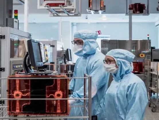
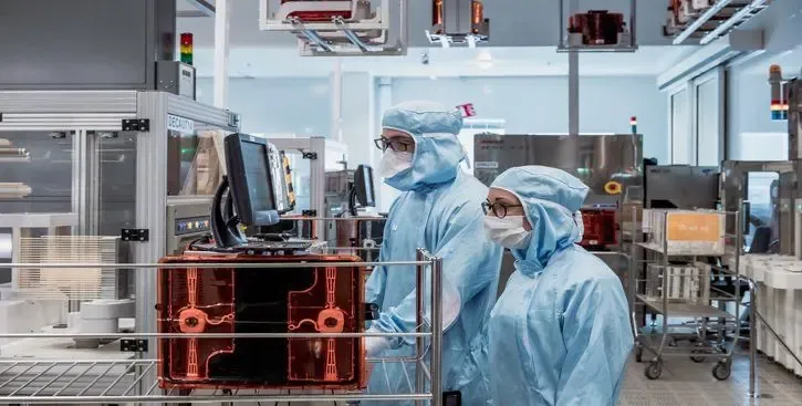
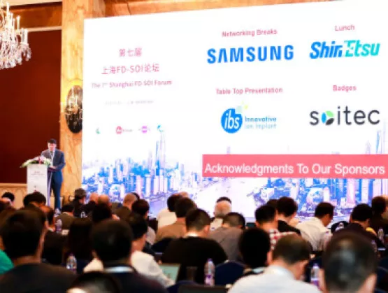
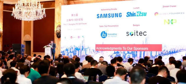
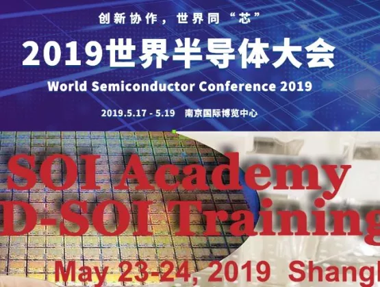
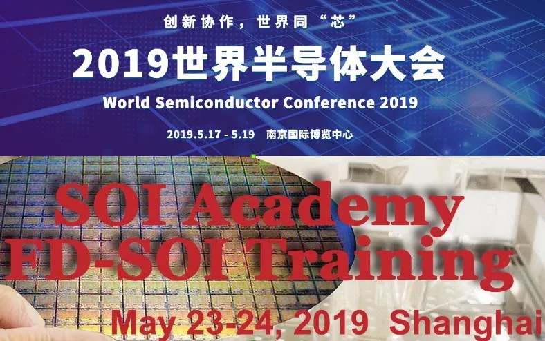
The first day of the SOI Consortium’s recent China event – the 7th Shanghai FD-SOI Forum – was full to bursting in every way: the room, the networking, the level of expertise, the in-depth presentations and the overall energy. We covered the Samsung and GlobalFoundry keynotes in our previous post (if you missed it, read it here).This post will recap the rest of the presentations given during the day. (If your company or institution is a member of the SOI Consortium, you’ll be able to access the full presentations online.)International Business Strategies (IBS) – Impact of AI on Automotive and IoT, and Opportunities in China (Handel Jones, CEO) When it comes to deep insights on China + tech + analytics, and especially with a thorough understanding of FD-SOI markets, Handel Jones is arguably the world’s leading expert. Here are some of the observations he shared. Though the chip industry will see declines across the board in 2019 (he sees 13.5%), he sees a return to growth in 2020. By 2030, he sees it as a trillion dollar market, of which China will have half. AI is a key driver – and will become more prevalent at the edge. Major drivers will include preventative medicine, gaming, NB-IoT and 5G. At the chip level, FD-SOI has a lower cost/chip compared to bulk – you’ve got small chips and high yields. Sensors – especially image sensors – are a key area, and this is another place where FD-SOI is better than bulk. He sees chip shortages in the 2022-24 time frame (as opposed to the current oversupply), so now is the time that China should be establishing large FD-SOI capacity.NXP – Automotive, Industrial and IoT Solutions Leveraging FD-SOI (Ron Martino, VP GM) 
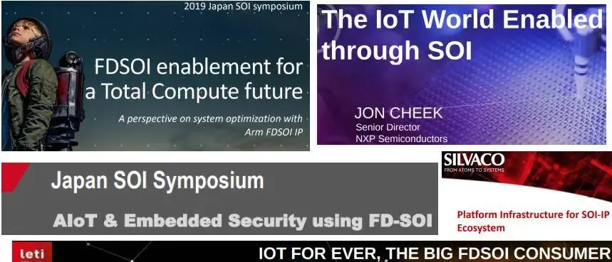
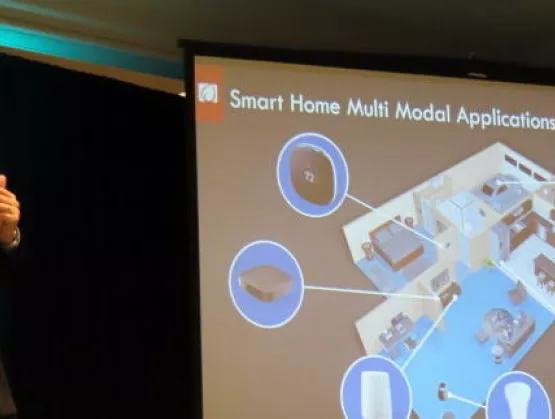
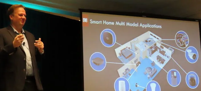
In terms of power consumption, computing is easy but data transmission is hard, Ron Martino reminded the audience at the onset. That’s why you need the edge. This is where FD-SOI comes in, and if you want to have leadership, you should be leveraging body biasing, he said. In terms of machine learning, a lot can happen at the edge on the smallest devices. NXP is now shipping a very wide range of products based on FD-SOI, including the i.Mx7 and 8 families and the new RT crossovers. The latest announcement is the i.Mx RT 1100 MCUs, a very low-cost processor solution for high volumes. The i.MX7 ULP is in mass production for wearables, with record low leakage and high performance. The i.Mx8 and 8x are going into a broad range of applications – from retail solutions for automated checkout to pasta makers, and automotive applications for full cockpits with vision detection, as well as things like parking, V2X and in-vehicle monitoring.Sony Semi – Low Power IoT Products with FD-SOI eMRAM Technology (Kenichi Nakano, GM) Chips built on FD-SOI with eMRAM are in production, said Kenichi Nakano. In GNSS/GPS, Sony is the #1 in lowest power consumption worldwide, thanks to FD-SOI, he continued. They’ve had 70 remarkable design wins, giving them over 50% market share in the sports and health watch markets, he said with a tip of the hat to the FD-SOI ecosystem and SOI Consortium. In GNSS, performance is very important – and now they can do it in water, which is huge. Development cycles are shorter than ever – for the latest chip it started in February 2018 and was in production by the spring of 2019, achieving decreases of 20% in power, 30% in area and 10% in cost. Integrating eMRAM was easy in terms of the design flow and manufacturing, with production yield of 97-100%. So with the GXD5605GF they’ve got the first GNSS chip with FD-SOI/eMRAM/RF in the world and it’s on 28FDS/eMRAM technology. It’s very reliable and very good, he concluded.Rockchip – Challenges of AIoT Chip (Feng Chen, SVP) At the beginning of this year Rockchip announced the launch of their RK1808, a low-power AIoT solution with built-in high performance (3TOPS) NPU fabbed in GlobalFoundries 22FDX, said Feng Chen. Their clients were very happy that Rockchip delivered the real power and performance numbers they’d promised. Because of the power/performance it delivers, FD-SOI (both 22 and 28nm) is very well suited for AIoT chips, he said. It’s very cost-effective in terms of NRE and die, and there’s room for further savings. While the ecosystem needs a unified push, FD-SOI is good for the market in China, and China has the volumes FD-SOI needs. Rockchip sees particular potential in retail and smartphones.Panel – Verticals Driving FD-SOI VeriSilicon CEO Wayne Dai moderated the first panel, asking first why China should adopt FD-SOI. Soitec CEO Paul Boudre said because it is a big, dynamic market (noting that Sony’s first FD-SOI GPS win was in China). Handel Jones said that at the wafer level, there was cost parity, but with FD-SOI chips are smaller and higher yield. The main reason it’s taken so long to get going was IP, but that’s changing now, he added. Dai’s next question was about the top application fields the panelists predicted for 2020. Sony’s Kenichi Nakano said wearables with connectivity, low power consumption, small size and high levels of integration; Rockchip’s Feng Chen agreed. NXP’s Ron Martino said FD-SOI for automotive, machine learning and edge computing was shipping now, with wearables ramping.VeriSilicon – Low Power IoT Connectivity IP Design Based on FD-SOI (Yi Zeng, Director, IoT Connectivity Platform) The “value” of IoT data is not yet being generated, noted Yi Zeng but AI can help here. The IoT industry needs innovation for both chips and networking. SiPaaS – which stands for Silicon Platform as a Service – as offered by VeriSilicon can help lower the barrier to entry. [In the SiPaaS model, VeriSilicon has its own IP-based core. Based on the company's advanced chip design capabilities and mass production service experience, it has created a variety of silicon-proven chip design platforms that can significantly reduce the customer's chip design cycle.] They have FD-SOI IP for NB-IoT, BLE, GNSS and sub-1 GHz. The BLE (Bluetooth) RF IP is a complete offering optimized for low power on GlobalFoundry’s 22FDX. The NB-IoT IP is also optimized on their 22FDX ZSPNano, an energy efficient general purpose MCU+DSP core on 22FDX. And they’ll have results of test chips for GNSS RF IP on 22FDX by the end of this year.Secure-IC – AIoT Embedded Security Using FD-SOI (Hassan Triqui, CEO) While AI enables products and services, it’s important to plan for security early in the design cycle, said Hassan Triqui. Software is not enough to protect edge-to-cloud. Secure-IC’s hardware security module, Securyzr, is an IP block that can be embedded into every device to answer security functionalities such as root-of-trust and key management. In sleep-mode/tunable cryptography, FD-SOI allows the creation of physically secure systems. (Note that designers are leveraging FD-SOI’s unique body biasing for ultra-low-power deep-sleep modes.) Because safety and privacy require a combined solution, Securyzer is particularly well-suited to IoT chips built on FD-SOI, he concluded, so that IoT adds value to AI, and not just the other way around.Soitec: FD-SOI – The 5th Gear for mm-Wave Radio (Michael Reiha, GM FD-SOI Business Unit) There are four key areas to 5G, explained Michael Reiha: coverage, number of antennas, frequency and traffic density. 5G mmW access architectures are currently inefficient in terms of power and performance, but FD-SOI is ready for 5G access as both an analog and hybrid beamformer. For MU-mMIMO (massive MIMO), the RF front-end modules (FEMs) and transceiver will fully exploit FD-SOI. Sensing, calibration and control enabling hybrid beamforming and multiple users is easy in FD-SOI. The adaptive body biasing on the horizon will reduce power of FEM mixed-signal circuitry, and be a disruptive technology.STMicroelectronics – Automotive MCUs in 28nm FD-SOI for ePCM NVM (Shan-Lin Liu, Automotive Marketing Manager) As a leader in the automotive market, ST has seen that increased data flows in automotive are driving demand for higher performance and bigger memory in automotive MCUs, said Shan-Lin Liu. ST has taken a unique approach to NVM with embedded PCM (phase change memory) on 28nm FD-SOI. This gives them energy-efficient, high-performance cores with larger NVM memories, and it’s already qualified up to auto grade-0. PCM (vs MRAM) is BEOL. It uses two cells, so it’s more reliable and is good at high temperatures, he said. With FD-SOI, they can go up to 165o, and it’s soldering compliant. The preliminary results of the first MCU chip are excellent. It’s now running in a car, replacing the previous generation 40nm eFlash product.Leti – Advanced FD-SOI for Edge AI (Emmanuel Sabonnadiere, CEO) To fully run artificial intelligence on the edge, research powerhouse Leti is working on an unsupervised learning neural network using advanced FD-SOI and a mix of other technologies. These include embedded non-volatile memory (NVM), 3D integration, and new design tools. Sabonnadière said this new approach is expected to exceed the performance levels of current digital deep learning with neural networks that are capable of handling time-domain signals, sound and speech—and may produce a first "killer app" for advanced SOI. AI will require compact and power-efficient circuits for the inference phase, when neural networks infer things based on new data they receive, close to the end user. The combination of FD-SOI, 3D integration, and NVM opens a path towards dedicated circuits with major performance improvement within the limited power budgets of distributed electronics. In Europe, he noted, privacy concerns are driving the move from the cloud to the edge. On the Leti roadmap, they’ve broken through the 10nm limit for FD-SOI, using strain and body biasing to compensate for transistor mismatch. Also of note: since 2016 Leti has had an ongoing collaboration with SITRI, the Shanghai Industrial μTechnology Research Institute, an international innovation center focused on globally accelerating the innovation and commercialization of More than Moore technologies to power IoT.GlobalFoundries – GF Fab 1 Dresden: Delivering Differentiation with FDX for the Future of Automotive (Thomas Morgenstern, SVP GM Fab 1) Dresden Fab 1, Thomas Morgenstern reminded the audience, is the biggest in Europe, where it is part of the Saxony ecosystem. GF is moving advanced mask-making to Dresden, which is the lead site and Center of Competence for FD-SOI. With the “pivot”, GF is providing platforms. Fab 1 is automotive certified for 22FDX (GF’s 22nm FD-SOI technology), with automotive tapeouts in 2019. “Automotive is a journey,” he said, of continuous improvement, and a mindset: it’s a zero defects culture. The ramp to volume production is well underway, with 26 tapeouts of 22FDX products this year – almost double that of last year. He showed high yield data of about a dozen products, adding that since the beginning of the year every tapeout was first-time right with decreased cycle time. The key specifications for 22FDX with eMRAM for Auto Grade-1 have all been demonstrated, and customer feedback has been excellent.Next: Shanghai International RF-SOI Workshop recap As you can see, it was a packed day for the FD-SOI part of the SOI Consortium’s Shanghai event. In fact the room was still packed at the very end of the day. Several hundred VIPs then headed out for the ever-popular and festive evening riverboat dinner cruise, where the non-stop networking continued.A big shout-out to our sponsors and supporters: VeriSilicon, Simgui, SIMIT, Soitec, Samsung, IBS Ion Implant, ShinEtsu, GlobalFoundries and NXP.The next day of the event was devoted to RF-SOI. That will be the subject of our next post.
Read More
Renesas, one of the world’s very top MCU manufacturers, is heralding its new FD-SOI based R7F0E017 for energy harvesting applications. In an in-depth article in the May 2019 edition of EENews Embedded, Renesas Product Marketing Manager Graeme Clark detailed the new chip, which is sampling this year. It’s a fascinating read, with lots of explanations about how SOI enables the cutting-edge features (like an integrated energy harvesting controller) – you won’t want to miss it. BTW, here at ASN we’ve been covering the origins of this technology since 2005.They call it SOTB, for Silicon On Thin Box, but it is indeed their flavor of FD-SOI. The work started at Hitachi in cooperation with Renesas with a paper that debuted at IEDM 2004, then moved along through the series of mergers that resulted in the offering at what is Renesas Electronics today. Here are some key quotes from the article:“The new SOTB process can now offer active mode current of less than 20 µA/MHz and leakage currents down to 150 nA, while still allowing the development of devices with reasonably high clock rates, large embedded flash memories and SRAMs on chip. This combination of integration and power consumption will make devices developed on this process ideal for energy harvesting applications. The result of this new process is that we can develop a new generation of microcontroller products.” “The use of the Silicon on Thin Buried Oxide technology on this new device has resulted in some unique low power characteristics. The first device has the following features and future devices using this process could offer even lower power consumption. Active current of 20 µA /MHz Standby Current of 200 nAADC operation 3 µA @ 32 kHz256 Kbyte SRAM with 1 nA / Kbyte standby current” “The R7F0E017 is able to run safely from a pure energy harvesting power source due to the operation of the Energy Harvesting Controller. The device can operate from a wide range of potential energy sources including solar power, vibration, pressure and temperature difference, and many others. The integrated energy harvesting controller, supported by very few inexpensive external components, completely manages the cyclic wake-up sequence of the microcontroller, only using the extremely low energy harvesting source current.”Click here to read the full article on the eenewseurope website.
Read More
If you’re going to Semicon West this year, be sure to attend the SOI Consortium’s workshop on how IoT is driving the SOI supply chain. There’s a great line-up of speakers – see the program below. IoT means many things to many people but everyone agrees it’s here and growing quickly. IoT, including machine learning and movement to the edge, is fueling innovation as the high compute and ultra-low energy requirements are pushing technology to deliver on these needs. The well-known characteristics defining IoT of “Sense”, “Compute”, and “Act” put additional burden on technology to full these requirements across a variety of use cases and environments without sacrificing reliability or quality. All the various forms of SOI technology from FD-SOI to High-Voltage to RF-SOI, are uniquely situated to deliver on the promise of today’s as well as tomorrow’s IoT roadmap. The supply chain for all forms of SOI technology is in place. This workshop will discuss the current and future solutions from a supply chain perspective.Speakers include experts from SOI Consortium members Applied Materials, NXP, GlobalFoundries and Soitec.Entitled The Internet of Things, Driver of the SOI Supply Chain, the workshop will take place at the Moscone Center South, Wednesday July 10th in Room 301. It will run from 1 pm until 4:30 pm. Anyone and everyone who is registered for Semicon West is welcome. Here is the sign-up page.It’s a great program: 1:00pm - Welcome by Semi1:10pm - IoT/AI/Edge Market – Using SOI Through-out, Jon Cheek, Senior Director, NXP1:35pm - The SOI Opportunity, Manish Hemkar, Director, Semiconductor Products Group, Applied Materials2:00pm - The Foundry IP Ecosystem, Jamie Schaeffer, Sr. Director, GlobalFoundries2:25pm - Engineered Substrates - Enabling the IoT Revolutions, Eunseok Park, Director, Emerging Technology in Strategic Marketing, Soitec 2:50pm - Enabling the SOI Era, Thomas Uhrmann, Head of Business Development, EVG3:15pm - Panel: The Internet of Things, Driver of the SOI Supply Chain, Moderator: Carlos Mazure, Chairman, SOI Industry Consortium. Panelists include:Manish Hemkar, Director, AMATYoshio Kitahara, President Managing Director, Kokusai EuropeThomas Uhrmann, Head of Business Development, EVGJon Cheek, Sr. Director, NXPThomas Piliszczuk, EVP Strategy, SoitecJon Kretzschmar, Manager of Product Sales Marketing, TEL America4:05pm - Closing remarks, Carlos Mazure, Chairman, SOI Industry Consortium4:20pm - EndThis is a great chance to learn more about SOI and the SOI Consortium. Don’t miss it!And while you’re at West, you should also check out a related event. SOI Consortium member Leti will be teaming up with Fraunhofer for a workshop entitled New Paradigms in Microelectronics–Providing R D for the 21st Century. That happens at the nearby W Hotel in San Francisco on Tuesday, July 9th at 5:00pm. Click here for more information on that.
Read More
Join us! In partnership with our members, the SOI Consortium is co-organizing and participating in two key SOI events coming up in China over the next few weeks. On May 18th, we’ve put together an SOI Forum at the World Semiconductor Congress (WCS) in Nanjing. And on May 23rd 24th, we’ve teamed up with our members SIMIT, Sitri and Leti for another in our series of SOI Academies, including an FD-SOI Training Day. (The last one this past winter was a terrific success – read about that here if you missed our coverage at the time.) QR code for WCS, Nanjing '19At WCS, the SOI Forum (sub-forum #8) is part of the afternoon Innovation Summit. We’ll cover the broader SOI ecosystem, including both RF-SOI and FD-SOI – from wafers to design through manufacturing. Presentations will be given by members of the SOI Consortium team, and by leaders from our membership, including Simgui, NXP, Incize, ST, IBM, Cadence and Xpeedic. Click here or scan the QR code for the full program and registration information. Also at WCS, SOI Consortium member VeriSilicon will be participating in a morning session on AI and IoT Wireless Communications (sub-forum #4). They’ll be giving a presentation on their low-power Bluetooth design platform for GlobalFoundries 22FDX, and their CEO Wayne Dai will be moderating a round-table discussion. You can get more information on that (in Chinese only, tho) here, or follow VeriSilicon on WeChat. QR code for SOI Academy and FD-SOI Training, Shanghaid 2019The SOI Academy in Shanghai is an opportunity for experienced designers to gain solid expertise in FD-SOI. The event begins in the afternoon of May 23rd with a series of informative plenary talks by members of the SOI Consortium team, and by experts from our members Leti, Soitec, VeriSilicon, GlobalFoundries and NXP. The FD-SOI Training starts the next morning, on May 24th.. This is a hands-on event lead by top experts from Leti. The morning is devoted to digital design in FD-SOI, and the afternoon to RF design (including for 5G) in FD-SOI. Attendees will get a comprehensive understanding of design techniques for low-power chips leveraging the multiple benefits and flexibility of FD-SOI technology. Get more information here, or from the WeChat QR code.We've got a busy schedule! To keep up to date with where we and our members will be promoting the SOI ecosystem, be sure to check our Events page regularly.
Read More
Key takeaway #2: If you need a Goldilocks process node – where you'll get just the right balance between active power, unit cost and investment – look to FD-SOI. And, btw, the IP landscape has improved dramatically. Those were just some of the great points made by Huibert Verhoeven (shown above), GM/SVP of Synaptics' IoT Division in his talk at the recent SOI Symposium in Silicon Valley.BTW, if you missed part 1 of our coverage --Silicon Valley SOI Symposium a Huge Success. Key Takeaways (Part 1) Here. – you’ll want to be sure to read it, too. Almost all of the presentations are now posted on our website – click here to access them.In this post here, we’ll cover presentations by Synaptics, GlobalFoundries, STMicroelectronics, Anokiwave and Dolphin Integration. It was a really full, day, so be sure to stay turned for Part 3 of our coverage to follow shortly: it will highlight the remaining presentations and panel discussions.Synaptics: Smart Home at the EdgeSynaptics’ Verhoeven’s presentation Revolutionizing User Experience Through Secure Neural Network Acceleration at the Edge was about Smart Home and using SOI. Synaptics is a human interface (HMI) company that’s been doing neural networks since 1986. They’ve always been on the leading edge, from their first shipment of PC touchpads to becoming a dominant force in all things HMI today: they now ship over a billion units annually. Synaptics slides 15 16 from the SOI Symposium, Silicon Valley 2019.They currently have SOI products shipping with dedicated neural networks for voice, he said. European [privacy] regulations have played a part in driving their use of SOI, as have challenges regarding power and heat. Things are getting smarter at the edge. For example, not only do users want their coffee machine to offer the usual morning espresso, Synaptics says that the next step is for your coffee machine to recognize you’re looking extra tired and ask if you might want a double?! For them Smart Home and multi-modal applications are the primary area of interest, as well as some automotive. Although their biggest customers have resources, others need guidance. Voice is a critical component, but now you also need video and display.Why SOI? Their HMI vision requires low power, significant computation and dedicated neural network hardware, explained Verhoeven, so FD-SOI with RF meets their needs. “22nm SOI is a Goldilocks IoT Process Node,” he proclaimed. It gets the combination of active power, unit cost and investment just right. What’s more, he said, “The IP landscape has improved dramatically. Our choice of SOI was not an accident.” Be on the lookout for more products leveraging FD-SOI over the next six months, he concluded. At this point on SOI, they’ve got 1 TOPS products with dedicated NPU for speakers, soundbars, Wi-Fi mesh, appliances, STBs and smart displays. These products have voice and sensor real-time (RT) AI. Next up is 4 TOPS on SOI with dedicated NPU, targeting STBs and smart displays with voice, video, imaging and RT AI. GF: World-Changing OppsGlobalFoundries slides 6 7 from the SOI Symposium 2019, Silicon Valley.“Our clients are at the forefront of changing the world,” declared Mark Granger, VP of the Automotive Product Line at GlobalFoundries. His presentation, Capturing High Growth Market Opportunities with SOI, detailed how mobility, automotive and IoT are the growth markets for SOI. So not unsurprisingly, GF’s 22nm FD-SOI technology, 22FDX, is seeing particular traction in mobile, edge, wearables and automotive. They’ve got twice as many tape-outs this year as they did a year ago, he noted. GF’s SOI portfolio includes 22FDX®, 45RFSOI and 8SW/7SW RF SOI for 5G/mobility; 22FDX for automotive (fully qualified for automotive Grade 2, with Grade 1 on the way); and 22FDX, 130RFSOI and 8SW/7SW RF SOI for IoT. GF has announced a stream of good news recently:with Dolphin Integration they’re delivering differentiated FD-SOI Adaptive Body Bias Solutions for 5G, IoT and automotive applications;they’ve crossed the billion-dollar design win threshold with 8SW RF SOI technology; they’ve collaborated with Synopsys to develop the industry’s first Automotive Grade 1 IP for their 22FDX process;and they worked with Rambus on the delivery of High-Speed SerDes on 22FDX® for communications and 5G applications.You might have heard about the Dolphin Integration news, as we covered it recently here at ASN (if not, be sure to read it here). Dolphin’s IP and methodology solutions address energy efficiency challenges. Automated transistor body biasing adjustment can achieve up to 7x energy efficiency with power supply as low as 0.4V on 22FDX designs. At the Silicon Valley event, Dolphin Integration CEO Philippe Berger provided additional information in his talk, FD-SOI IP Platform for Energy-Efficient IoT SoC. Dolphin Integration slides 5 6 from the SOI Symposium 2019, Silicon Valley.In another GF-related talk, Nitin Jain, the CTO of longtime GF RF-SOI customer Anokiwave presented Unleashing the mmWave Phase Array Using SOI for 5G Satcom. Anokiwave is a fabless semi IC company (you’ll find a good technical discussion of mmWave phase array written by their Chief Architect here). They do active antennas (aka phased array), something the military’s done for a long time, but now Anokiwave is bringing it to new markets and applications including radar, satcom and 5G. What they’ve been able to do is planarize the active antennas. They use GF’s 45RFSOI process technology for phased array systems because of the cost, performance, scalability and system enhancements it enables. 45RFSOI, he explained, is ideal for beam-forming FEMs (including the switches, LNAs and PAs). The move to 5G/mmWave is going to require a lot of antennas, so these Anokiwave ICs are headed to high volumes, concluded Jain.Stellar by STAs Roger Forchhammer, Director of Business Development at STMicroelectronics pointed out in his presentation, Automotive FD-SOI Microcontrollers with Embedded PCM, ST pioneered FD-SOI (and that was almost a decade ago, btw). Then in February 2019, they announced a world first: they’d begun sampling 28nm FD-SOI microcontrollers (MCUs) with embedded non-volatile memory (eNVM) based on embedded Phase-Change Memory (ePCM) to 10 alpha customers. These MCUs target powertrain systems, advanced and secure gateways, safety/ADAS applications, and vehicle electrification.STMicroelectronics slides 9 10 from the SOI Symposium 2019, Silicon Valley.(In case you want technical details, the breakthrough ePCM eNVM was first presented at IEDM in December 2018 – you can get the presentation that accompanied the paper, Truly Innovative 28nm FDSOI Technology for Automotive Microcontroller Applications embedding 16MB Phase Change Memory, from the ST website.)In his Silicon Valley presentation, Forchhammer said they’re now doing Stellar, a whole family of automotive products on FD-SOI. To do it, they’d taken an existing device and moved it to 28nm FD-SOI with ePCM, which they manufacture at their fab in Crolles, France. A major advantage for automotive he cites is that in software updates it’s bit-level programmable. “ST is fully behind FD-SOI,” he concluded, adding that we’re see more automotive as well as IoT products coming soon. Well folks, that’s all for this post. We’ll finish up our coverage of the SOI Consortium’s 2019 Silicon Valley Symposium in the next ASN post (there was so much to cover!). So please stay tuned.
Read More
Two of the big, recent breakthroughs in memory technology – eMRAM and ePCM – have gotten their start in volume manufacturing on 28nm FD-SOI. In conjunction with the 2019 IEEE International Memory Workshop, SOI Consortium members Leti and Applied Materials have teamed up to give a technical program to explore short-term and long-term memory solutions. While the workshop is not specific to SOI, given the recent foundry announcements about ePCM and eMRAM for FD-SOI, the organizers predict it will be of particular interest to those following the greater SOI ecosystem. The event takes place at the end of the Sunday IMW tutorial day, starting at 5:30pm at the Hyatt Regency in Monterey, CA. Please see this page for the program and registration information. Here is the program: Emerging Non-Volatile Memory Promises Toward New Energy-Efficient Design and Applications - Michael Tchagaspanian, VP Business Development, CEA-Leti Technologies That Enable MRAM and PCRAM in Volume Manufacturing - Kevin Moraes, Vice President, Metal Deposition Products, Applied Materials Technology Improvements Directions of Emerging Non-Volatile Memory for New Applications Solutions - Etienne Nowak, Head of Memory Laboratory, CEA-Leti Integration Schemes and Challenges for New Memories in a New Artificial Intelligence Era -Michel Frei, Director, Advanced Product Technology Development, Applied Materials Jean-Eric Michallet, Head of Leti’s Microelectronics Components Department, Silicon Component Division is one of the organizers. Here is his overview: FD-SOI is expected to be a long-lived technology. It enables planar CMOS scaling and accommodates a great deal of More-than-Moore developments where its ability for low power and great analog performance can make a difference for IoT, Automotive, Machine Learning or 5G applications. But to do this it requires a high-performance and cost-effective non-volatile embedded memory option. The incumbent Flash cell is reaching the end of its roadmap due to the difficulty of shrinking the bitcell and manufacturing, as well as the finished wafer cost increase. Back-end integrated Random Access Memory in advanced CMOS process has been explored for many years now as a competitive solution for fast-write and low-voltage non-volatile embedded memories. Foundry availability of embedded Magnetic RAM and Phase Change RAM for FDSOI 28nm platforms has been announced recently, showing that these technologies have now reached industrial maturity. CEA-Leti and Applied Materials invite you to attend a technical program to explore short-term and long-term memory solutions, from early research to industrialization. Registration is open, free, and available to all IMW attendees, and others. However, as seating is limited and as we have already several participants pre-registered, registration is by invitation only and early registration is recommended. If you are interested, please email Jean-Eric Michallet. The event is presented in conjunction with the 2019 IEEE International Memory Workshop, to be held on Sunday, May 12th, 2019, Hyatt Regency, Monterey CA, starting at 5:30 pm.
Read More
Editor's note: Arm and Samsung Foundry are extending their collaboration on FD-SOI, which they'll be highlighting at the SOI Consortium's Silicon Valley Symposium April 9th. In the meantime, Arm Senior Product Marketing Manager Umang Doshi described the range of projects in a recent Arm Community / Developer physical IP blog. We thank Arm for sharing this blog with ASN readers.~ ~~ Samsung Foundry and Arm FDSOI collaboration announced By Umang Doshi The challenge with designing at newer and more advanced process nodes is that things generally don’t get less complex and expensive, much as we might want this. Still, the upside to each new process node, generally, is that you can build more highly efficient and targeted devices to address more markets and applications in a timely fashion. For the complexity and cost challenges, however, there’s good news: Arm and Samsung Foundry just announced a comprehensive, foundry-sponsored physical IP platform, including an eMRAM compiler at 18FDS (18nm FDSOI). In addition, the Arm offerings for 18FDS include three POP IP packages for Arm Cortex-A55, Cortex-R52 and Cortex-M33 processor IP. The platform will help drive new leading-edge designs in power-sensitive applications in 5G, artificial intelligence (AI), automotive, Internet of Things (IoT), and other market segments. It’s the industry’s first, fully comprehensive physical IP platform that includes an eMRAM compiler at 18FDS. 28nm: Before the breakthrough One of the most widely embraced nodes, 28nm the so-called “forever node,” has done wonders for industry innovation over the years. However, leakage power is still challenging for planar transistors. Engineers deployed high-K metal gate (HKMG) at 28nm, to combat leakage, but it’s still an issue. That’s because the channel underneath the gate is too deep and too far from the gate to be well-controlled, which results in higher leakage power. Solutions for the leakage issue have prompted designers to embrace FinFETs and FDSOI (fully-depleted silicon-on-insulator) with thinner channels that enable greater control by the gate. Indeed, FDSOI is gaining traction in the market place. By construction, 28nm FDSOI enables much better transistor electrostatic characteristics versus conventional bulk technology. 28nm FDSOI offers: Wide Forward/Reverse Body-bias range and flexible Poly bias (PB) range to tradeoff power/performance. Better performance and power than bulk process technology. Better resistance to radiation and SER. Less sensitive to variability because there’s no channel doping. Ultra-low power voltage (operating at low voltages in the hundreds of millivolts range). Easy migration from bulk versus the previous SOI version, PDSOI (partially-depleted silicon-on-insulator), required unique timing and power models. What’s more, there are cost benefits today and more forecast for the future. Arm and Samsung Foundry extend FDSOI leadership from 28FDS to 18FDS In 2018, Arm announced the industry’s first Embedded MRAM (eMRAM) compiler IP built on Samsung Foundry’s 28FDS process technology. Since the announcement, Arm has engaged with several Samsung Advanced Foundry Ecosystem (SAFETM) partners on a landscape-changing collaboration to deliver the industry’s first 28FDS eMRAM-enabled IoT silicon system demonstrator telling the Arm IoT story on Samsung Foundry silicon. Coupled with Arm’s IoT ecosystem, Pelion IoT Platform and Platform Security Architecture (PSA) solutions, this 28FDS eMRAM-enabled IoT demonstrator will showcase a new-generation of secure and energy-efficient IoT edge devices which integrates software stacks offering secure boot, firmware updates, on-chip storage, chip to cloud communication and device/software provisioning. The combination of 28FDS and eMRAM non-volatile memory brings new opportunities for a new class of highly integrated and energy-efficient designs. We’re thrilled that Samsung Foundry has extended its successful collaboration on FDSOI technology from 28FDS process to 18FDS. With the new platform, 18FDS is a cost reduction solution with lower power and same back end of line (BEOL) as 14nm FinFET. It has RF and eMRAM support to enable the widest range of different applications. “18FDS is the next-generation node on Samsung's FD-SOI roadmap with enhanced power, performance, and area (PPA)," said Jaehong Park, executive vice president of Design Platform Development at Samsung Electronics. “The relationship between Samsung Foundry and Arm stretches back more than a decade and has helped put the right design technology in the hands of the world’s leading designers. The enhanced PPA from our 18FDS process combined with Arm cores and Artisan Physical IP will again bring the cost and time-to-market advantages to enable the competitive and differentiated SoC designs.” Highlights on Arm-Samsung 18FDS platform Includes seven memory compilers, three logic libraries, two (1.8 and 3.3V) GPIO libraries, three POP IPs and the eMRAM memory compiler. Supports automotive AEC-Q100 Grade 1 design requirements, and comes with ASIL-D support and a complete automotive safety package. Utilizes back biasing supported by the FDSOI technology to help achieve low leakage by using reverse body-bias technique or a performance boost using forward body-biasing. This is a key differentiation of 18FDS platform. Supports Logic Corner Generator (LCG) and Memory Compiler Corner Generator (MCCG). LCG and MCCG products allow designers to generate custom corners with body-bias voltages to take the maximum advantage of body biasing power-performance flexibility. 18FDS will help enable the development of new devices connecting consumers in entirely new ways, whether it’s in AI, 5G mobile, automotive or other areas. The platform will be available in late 2019. Arm's Physical Design Group has a track record of successful implementations with Samsung Foundry across multiple generations of process nodes and products. Besides 28/18FDS, Samsung Foundry and Arm also have 14LPP/LPC, 11LPP, 7LPP and 5LPE platform collaborations. Interested in knowing more about Artisan Physical IP at 28/18FDS? Come join us at SOI Silicon Valley Symposium on April 9 at Double Tree by Hilton, San Jose, California. During the event, you will have the opportunity to hear how Arm and other industry leaders work together to accelerate the adoption of FDSOI technologies including products and applications. Alternatively, you can also reach out to us with your inquiry.
Read More