downloadGroupGroupnoun_press release_995423_000000 copyGroupnoun_Feed_96767_000000Group 19noun_pictures_1817522_000000Member company iconResource item iconStore item iconGroup 19Group 19noun_Photo_2085192_000000 Copynoun_presentation_2096081_000000Group 19Group Copy 7noun_webinar_692730_000000Path
Skip to main content
Default Banner Image

machine learning

SEMI Releases latest update to World Fab Forecast with adjusted semiconductor revenue consensus for second-half 2018 and 2019 Global semiconductor revenue in 2018 is now expected to reach $473.8 billion and clock a growth rate of 15 percent, a significant upward revision from the 7.5 percent expansion (to $442.9 billion) forecast at the start of the year by six research and investment forecasts tracked by SEMI Industry Research and Statistics (SEMI IR S). Data center growth will remain robust in the coming quarters, fueling demand for memory devices. In addition, cloud computing will continue to spur strong CPU, GPU, networking, ASIC, and DRAM and NAND demand through 2019, driving a consensus 3.63 percent year-to-year growth to reach the semiconductor revenue of $491 billion in 2019. Fab equipment spending (new and used) for 2018 is expected to increase by 14 percent to a record high of $63 billion, according to the last data from the SEMI World Fab Forecast, published by SEMI IR S. For 2019, fab equipment spending (new and used) is expected to increase 8 percent to another record of just under $68 billion. Memory continues to be the biggest swing factor in fab spending in 2018 and is expected to lead growth into 2020. 3D NAND will see the most capacity added in 2018 and 2019 with growth of 41 percent in 2018 and 27 percent in 2019, according to the SEMI World Fab Forecast. DRAM investment will see even stronger growth in 2018 and 2019 driven by new capacity addition as well as the continued technology shrink towards 1y/1z nm. For the first half of 2018, global spending for semiconductor fab equipment continues its growth momentum from 2017. Though we expect some softness in the second half of 2018, the outlook for 2019 remains robust with a fourth consecutive year of growth – the first such run since the 1990s. This prolonged growth cycle has been propelled by memory and will be extended by significant investment in China in 2019. Although a potential slowdown in 2020 is a concern, the overall outlook for semiconductor demand remains solid due to broad-based growth trends in data center, artificial intelligence (AI)/machine learning (ML), automotive, and industrial segments. Following are other SEMI forecasts for fab spending. Installed Capacity 3D NAND will see the most capacity added in both 2018 and 2019 with growth of 41 percent in 2018 and 27 percent in 2019. Foundry capacity growth is steady at 3 percent in 2018 and 6 percent in 2019, driven by both leading-edge and trailing-edge capacity buildup. 200mm fab capacity will increase 4 percent in 2018 and 3 percent in 2019, fueled by demand for MCU, sensors, PMIC, MOSFET and Driver IC. New Facilities / Construction Spending In 2018, there are 72 construction projects with investments totaling $15 billion, a year-over-year increase of 23 percent. Construction spending will reach all-time highs with China continuing its lead at US$7 billion in 2018, shattering its own record of $6.3 billion investment in 2017. Most construction spending in 2018 will be for Memory (just under $9 billion), primarily for 3D NAND followed by DRAM. Foundry will log second place in construction spending at just under $5 billion. Fab Equipment Spending Fab equipment spending (new and used) for 2018 is expected to jump 14 percent to a record high of US$63 billion, flat from the forecast issued in June 2018. Equipment spending (new and used) for 2019 is expected to increase 8 percent to another record of just under US$68 billion, a downward adjustment from +9 percent published in June 2018. We believe equipment spending will remain healthy, driven by solid, broad-based demand and predictable technology investments on top of constructive SEMICAP equipment fundamentals. Activity Report The August report features 1,265 records including about 300 Opto- and LED-related facilities. We have made 223 changes related to 216 fabs/lines. The modifications include the addition of new records, changes to existing records, the deletion of records since the February 2018 World Fab Forecast report. We are tracking 103 future facilities/lines with various probabilities that will start volume production in 2018 or later. Download a sample report Not a subscriber? Please review SEMI fab databases listed below. Our databases deliver the latest forecast and a complete analysis of front-end fabs and foundries worldwide. They are ideal resources to empower your market research. Eugenia Liu is a Senior Product Marketing Manager at SEMI.
Read More
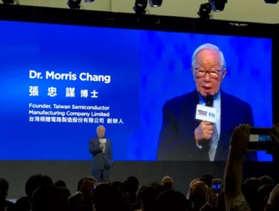
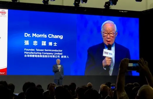
Over the past three decades, most of the world’s innovations have centered largely on business models and involved iterative advances of existing technologies, with none matching the global impact of the top 10 semiconductor industry discoveries and advances, Dr. Morris Chang, founder of TSMC and the IC foundry model, said at SEMICON Taiwan 2018 this week.Few have as clear a perspective on the transformative power of semiconductors as Dr. Chang, founder of TSMC and father of the IC foundry model. Keynoting the IC60 Master Forum celebrating the 60th anniversary of the invention of the integrated circuit (IC), Dr. Chang listed what he considers the 10 key semiconductor industry innovation milestones since 1948:1. Invention of the transistor by Shockley, Bardeen, and Brattain – 19482. Silicon transistor – 19543. Integrated circuit – 19584. Moore’s Law – 19655. MOS technology MOS FET – 1964 Silicon gate – 1967 CMOS – 1970 6. Memory DRAM – 1966 Flash – 1967 7. Outsourced assembly and test (OSAT) – 1960s8. Microprocessor – 19709. VLSI systems design – 1970-1980 IP and design tools – 1980-present 10. Foundry model – 1985 Among the most consequential semiconductor advances may be yet to come, Dr. Chang said, citing innovations including artificial intelligence (AI) and machine learning, new device architectures, Extreme Ultraviolet lithography (EUV), 2.5D/3D packaging, and new materials such as graphene and carbon nanotubes.Dr. Chang argued that because bringing an innovation into production is immensely more expensive than proving a theory in a lab, innovators are not always the ones to implement and benefit from their novel ideas. Today, innovation costs are skyrocketing, driving more consolidation across the supply chain.Michael Droeger is director of marketing at SEMI.
Read More
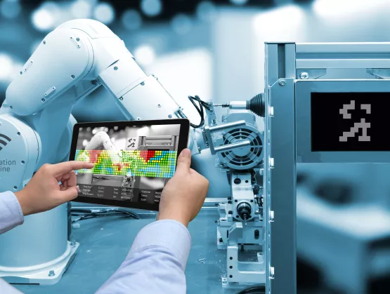
What’s next for smarter, more connected electronics manufacturing - Part 3 The fast-maturing infrastructure now enabling analysis of exponentially larger data volumes brings the microelectronics industry to an inflection point, where the winning companies will be the first to master the use of this data to solve the industry’s emerging challenges. SEMI expands its coverage of these vital issues with a Smart Manufacturing Pavilion and three days of talks SEMICON West, July 10-12 in San Francisco. While deep learning is starting to be applied to image recognition for wafer inspection, it is also being considered for sequential pattern recognition in order to evaluate equipment parameter traces. The next emerging applications will start to use those learned patterns to predict outcomes, and then use those predictions to automate process control. One early application of deep learning is IC process development. “People don’t think of research and development as the first place to automate, but it’s where applying our digitization and simulation has first had impact,” says David Fried, Coventor vice president of Computational Products. He noted that insertion is easier in the lab than in the fab. Technology at 10nm and beyond is now so complex that companies at the leading edge must use process modeling to understand the effect of process variation on their designs. Learning cycles can now be accelerated during development by simulating 10,000 digital wafers instead of running 25 actual wafers during screening, Fried says. Applying structured analysis and machine learning to the data simplifies optimization across the 500 or more interrelated process steps. Coventor has recently introduced a statistical analysis package that aids the design and analysis of process variation experiments by using large volumes of data from its models. Fried says these models are next being used to accelerate the yield ramp in manufacturing. Digital simulation also could speed development of high-mix, lower value products While digital twins are best known for their use in complex, high value products like jet engines, the simulation technology could also enable the electronic manufacturing services (EMS) sector to reduce the time, cost and risk of developing its high mix of products. “The EMS sector’s use of digital twins will be vital for it to smooth the move of CAD/CAM digital design data for so many different products into manufacturing, and to accelerate validation testing of designs and products by doing more of it in the virtual world,” says Dan Gamota, vice president of Engineering and Technical Services at Jabil. Gamota also highlights the push for traceability from the automotive and healthcare markets, where the digital models could be used to quickly assure that the design was built exactly as specified. “In the past year, traceability has evolved from just ‘nice to have’ to ‘how to achieve,’” he adds. “Companies are expecting it, but aren’t willing to accept the cost and risk of doing it alone. We need the community to discuss realistic implementations, identify the most critical elements and bring together the ecosystem partners to build baseline reference architectures for key digital building blocks. The community also needs to assure the reliable flow of data among the electronic manufacturing segments from semiconductor to OSAT to EMS.” Predictive maintenance and virtual metrology applications could mature in next few years While predictive maintenance initially seemed a likely early application of machine learning in factories, it remains a challenge for the electronics sector. “The difficulty is that it’s not clear where to get the most bang for the buck,” says Tom Ho, president of BISTel America, noting that it may make the most sense to track the failure performance of a single expensive part, like an electrostatic chuck, since predicting the failure performance of a whole complex system like an etcher is much harder. “Collecting enough data from all failure types, including especially the rare events, is difficult unless you have a long history of a lot of tools,” adds Doug Suerich, PEER Group product evangelist. “The gain from collecting performance information from many tools across the industry could be big, but many companies still need to overcome concerns around exposing their IP.” Another big opportunity for prediction is virtual metrology – predicting the wafer outcome from the process or sensor data with enough accuracy to replace the physical metrology. “Virtual metrology is improving, and since metrology can be slow and expensive, any reduction could mean a huge potential savings,” says Suerich. “But it is still seen as too scary for many companies. Two to three years from now, companies will expand the practice from lower risk areas into processes that require more confidence in the results.” Moving beyond prediction to automated control needs digital models Once the results are predicted, the model can be used to control or automatically optimize a process and enable the system to learn by itself, usually by reinforcement learning on a digital model. The model can then independently make adjustments to optimize the manufacturing process. “Automated process development is getting close now. Instead of smart guys turning the knobs, deep learning is automating the smart tuning,” says Suerich, suggesting the industry could see widespread adoption in as little as two to three years. This type of machine learning needs a good digital model, and masses of data for learning. One approach uses human experts to build a physics-based model of the clearly understood parts of the process, then turns to deep machine learning to optimize the lesser-understood variables. The alternative, the data-first approach, runs a computer algorithm to suggest the solution purely from data, without human input, and then relies on the human to evaluate the usefulness of the results. Modeling digital twins of wafers could enable automated process control, chamber matching, and fleet matching, says Fried. If every wafer had its own virtual twin with all the upstream metrology and structural information needed to make equipment control decisions, it could feed forward that information to enable the seamless transition from one step in the process to another based on understanding their complex interrelationships. This could potentially improve uniformity across wafers and equipment, and reduce the need for metrology, he argues. Moving metrology sensors into the chamber will also require model-based algorithms to enable dynamic process control in close to real time, says Fried. These algorithms will be needed to acquire, parse, and process the data at high speed, and then to choose how to adjust the controls. “There will be a model behind collecting and interpreting the metrology data,” he notes. “That’s a really rich vein for improvements in process control.” “The end goal is to collect equipment data in real time, analyze it with AI, and send back controls to optimize manufacturing processes,” Jabil’s Gamota says. “This requires a robust architecture for communication between equipment and consistent formats for data collection and analysis. But the cost and complexity of this heavy lifting is too great for any one company to do alone. We need a consensus-based architecture for ingesting, analyzing and acting on the data.” SEMI tests data transfer protocols, benchmarks best practices SEMI is launching a smart data project to identify the various data transfer protocols needed for inter-company communications. The project will feature a proof-of-concept model in a development fab to produce verifiable results so SEMI can better understand how different approaches meet member needs. SEMI’s smart manufacturing technology communities and the Fab Owners Alliance are also benchmarking current smart manufacturing practices in the microelectronics industry to help SEMI members better understand the path forward and potential return on investment. Speakers over all three days at SEMICON West addressing these issues include Active Layer Parametrics, Applied Materials, Applied Research Photonics, ASML, Bosch Rexroth, Cimetrix, Coventor, ECI Technologies, Edwards Vacuum, Final Phase Systems, GE Digital, Infineon, Jabil, Lam Research, Osaro, Otosense, PEER Group, Qualcomm, Rockwell Automation, Rudolph Technologies, Schneider Electric, Seagate, Siemens, Stanford University, TEL, TIBCO Software. See semiconwest.org. What’s next for smarter, more connected electronics manufacturing - Part 1 What’s next for smarter, more connected electronics manufacturing - Part 2 Paula Doe, SEMI
Read More
Part 2 of this two-part piece examines the potential benefits to be realized by pairing human Subject Matter Experts with smart silicon assistants, and what these new arrangements mean for semiconductor device manufacturing. Part 1 explores best-practice perspectives on collecting and utilizing smart data in industries outside semiconductor manufacturing, one of the important takeaways from the Smart Manufacturing panel discussion at SEMI ASMC 2018. So what does this observation (i.e. the field of medicine, in what seems at first glance a big data environment, is really just clusters and clusters of loose small data connected by the collective neural network of highly trained doctors and their colleagues) mean for semiconductor manufacturing? We think it means we need to apply the same level of intense focus that we already devote to instrumented data collection and analytics in the fab to something more: we need to better capture the vast expertise of our engineering and operational talent in semiconductor manufacturing. We think we need to record what the subject matter experts (SMEs) in the fab see, hear, and think as they investigate yield excursions or machine-down problems. We need to effectively combine product, process, equipment and component subject matter expertise / subject matter experts (SME) with big data analytics to more effectively solve manufacturing problems, be they killer or be they chronic. And we must provide structured methods for incorporating inputs from and active participation of SMEs throughout the data analysis lifecycle, from collection and aggregation, through filtering, feature extraction, analysis and optimization. Some of the challenge will be in just how do we make it easy to gather information from SMEs in real time, while standing in front of equipment in the fab. Internet of Things (Iot) devices are emerging to capture and label images and sounds to enable machine learning algorithms to recognize and help diagnose manufacturing problems based on sight and sound, complementing the instrumented data. But we also need to record the thought processes our human SMEs go through in those investigations – perhaps by the SMEs talking to a smart AI-based conversational assistant who helps make “rounds.” Doing contextual analysis on this added data, combined with the instrumented data, will create the equation Human + Machine = AI (Awesome Insight). Sounds reasonable, right? We think artificial intelligence becomes too artificial if you leave the human out of the equation. AI should be augmented intelligence, where we take the expertise and creativity of the human, and combine it with the rapid computational capabilities of the computer, in order to put problem identification and solutions on steroids. But with the already huge advancements to date in data analytics, cloud, and the emergence of AI, why do improvements in quality, machine utilization, and the implementation of predictive analytics in semiconductor manufacturing seem to be creeping along incrementally, and not appearing as dramatic, step-function improvements? Call it Smart Manufacturing, call it Connected Enterprise, call it Advanced Manufacturing, or Analytics, or Cloud, or the Digital Twin … there are no shortages of terms, philosophies, and technologies available, but why aren’t we seeing their rapid adoption? It could be it’s the downside that comes with needing people. “Good business leaders create a vision, articulate the vision, passionately own the vision, and relentlessly drive it to completion.” Jack Welch. We see from other industries that smart manufacturing conversations originating with the executives of a company thinking to implement smart manufacturing programs lead to vision; however, we also see from other industries, and from our own, that realizing this vision has often been a challenge. Why is that? One reason may be that the people who are personally vested in solutions they implemented in the past, as well as those who follow a pattern of ‘how we’ve always done things’, create, inadvertently or not, persistent internal barriers hindering innovative action. Another may be that engagements with the working engineers and managers charged to be smart manufacturing implementers leads to the pursuit of low-hanging fruit, and cautious investments, that often utilize solutions that ultimately cannot scale and integrate. Not to mention the disadvantage of dealing with the legacy equipment, the legacy networks, the traditional thinking, and the lack of consistency in metrics adding to the confusion. Addressing all these barriers requires an alignment in strategy and execution, along with a plan to support the overall vision, often across the entire enterprise, which is no small matter. And then there are the standards. Having and adhering to standards in control solutions, networks, and data becomes critical in achieving real benefits from smart manufacturing. And data security. One of the other big impediments in the smart manufacturing transformation is data and IP security, another key concern (maybe the most significant) preventing us from moving forward more quickly (e.g. to cloud-based solutions) in our industry. More about that in a follow-up. Achieving synergy across all of manufacturing, from connecting equipment horizontally, through the production system (machines processes), and vertically, through enterprise systems and across production facilities, can only occur if we build standards, security, infrastructure, and human engagement throughout our ecosystem and supply chain. In simple form, the steps to do so include connecting assets, collecting and contextualizing data, and then driving business transformation with actionable insights gained from the data. With impact on every function, and every person, in the enterprise, from equipment operators in the fab through the C-Suite in HQ. Maintenance, Engineering, R D, Operations, Scheduling, IT, Procurement, Finance, HR all contribute, collaborate and benefit. Regardless of the technology, from device level analytics to predictive maintenance and optimization, the people that reside in these disparate groups need to come together with the smart machines to create a common strategy to achieve transformational results. Aligning an enterprise’s goals with its human capital is paramount to success. Therefore, we must challenge our team members and ourselves to work outside our comfort zones, and we need to be forever aware of the need for us to grow with the technology. Smart manufacturing is not necessarily about having fewer people in the fab, but it does suggest having people in the fab, perhaps with different, or upgraded, skill sets, who are even more efficient in their roles as a result of the boost they are getting from Industry 4.0. Fortunately, we now have techniques that let us combine the best, brightest, and latest and greatest analytics with our invaluable SMEs throughout the data analysis lifecycle. We’ll not only be able to deliver higher quality semiconductor manufacturing solutions all in all, but we’ll also be providing methods to more easily distribute, scale, maintain, and continually refine those hard-earned solutions. We expect that subject matter experts will continue to put the “smart” in machine-based smart manufacturing today, and for the foreseeable future. SME contributions are not an option, but, rather, an imperative for ensuring a semiconductor manufacturer’s sustained prosperity, much less its survival. Nancy Greco (IBM Watson), Dave Mayewski (Rockwell Automation), James Moyne (University of Michigan / Applied Materials), and Paul Werbaneth (Intevac, Inc.), along with Julie Jacob (Ernst Young), and Carson Henry (Micron Technology), were members of the SEMI ASMC 2018 panel discussing Industry 4.0 and the Future of Commercial Semiconductor Device Manufacturing. All opinions here are purely our own. Please contact Paul Werbaneth via email at [email protected]. The SEMICON West (July 9-11, 2018, in San Francisco) Smart Manufacturing Pavilion features working production equipment on the floor and three full days of speakers providing insights on building the infrastructure needed to enable AI. Equipment from Bosch Rexroth, Cimetrix, Rudolph Technologies, INFICON, Final Phase Systems, OMRON, DISCO and Edwards Vacuum will showcase cutting-edge smart manufacturing technologies. For information on the SEMI Smart Manufacturing initiative and how to get involved, please click here.
Read More