downloadGroupGroupnoun_press release_995423_000000 copyGroupnoun_Feed_96767_000000Group 19noun_pictures_1817522_000000Member company iconResource item iconStore item iconGroup 19Group 19noun_Photo_2085192_000000 Copynoun_presentation_2096081_000000Group 19Group Copy 7noun_webinar_692730_000000Path
Skip to main content
Default Banner Image

machine learning

Machine learning (ML) and artificial intelligence (AI) have ushered in tremendous opportunities for faster growth, problem-solving and technological development in the electronic system design ecosystem. Cadence Design Systems, Inc., a member of the ESD Alliance, a SEMI Technology Community, is at the technological forefront in incorporating ML techniques in its chip design products. I spoke with Chin-Chi Teng, Senior Vice President and General Manager of Cadence’s Digital Signoff Group, about how ML is reshaping EDA and the semiconductor industry, the cloud’s role in the evolution of ML in design and its impact on Moore’s Law. Teng also offers advice on how engineering students can calibrate their education to prepare to work with this transformative technology and urges them to have fun in the process. Smith: How is ML changing the EDA industry? Teng: ML is changing EDA for the better in many ways. It’s more difficult than ever to design chips, and ML is helping by overcoming the complexity, size and technology interdependencies. At the same time, ML is helping our own engineers solve certain classes of EDA algorithm, tool, and flow/solution challenges so that we can deliver even better EDA tools to our user base. The benefits can include reducing runtime, increasing quality of results, and being better equipped to manage vast complexity and data. Also, and maybe even more significant, is the potential boost to user and team productivity, where engineers have more time to focus on high-value problems because they no longer need to spend time on managing overwhelming volumes of data and details that can be easily automated. Smith: What is the potential impact ML can have on semiconductor design? Teng: ML technology can be leveraged in several ways to improve EDA tool performance and engineering team productivity. For example, we initially applied ML to applications such as formal verification, simulation regressions, analog circuit design, and PCB design. We targeted ML toward specific algorithms that processed lots of data to sharpen and speed decision-making. Then we started to look at digital implementation flows that combine multiple steps with multiple decisions in a recipe, especially for chip implementation where the more efficient use of engineering knowledge can make a substantial difference in the chip’s resulting power, performance and area (PPA). These flows present more challenges and require different ML and optimization techniques since the data points are expensive to create and the volume of data is huge. But flow optimization offers the largest rewards for companies investing in data collection and analysis to improve their operations and product quality. By using ML to improve the implementation flow, our users are seeing up to 20% better PPA and 10x improved productivity in developing data center CPUs and AI engines, automotive sensor processing SoCs, and mobile devices. Smith: What is the cloud’s role in the evolution of ML in EDA? Teng: More ML usage means there will be an inevitable surge in compute demand resources, and engineers need the ability to scale in parallel. The cloud provides engineers with the best opportunity to scale computing resources without facing procurement limitations. The cloud also allows engineers to use task-specific compute and ML accelerators and capitalize on distributed computing innovations that leverage the cloud for greater design flexibility and availability. Smith: You have written that you see Moore’s Law accelerating. How does ML fit into this? Teng: We see the rapid adoption of new process technologies as the biggest trend surrounding Moore’s Law right now. ML technology in EDA will help speed tool certification processes, process design kit (PDK) development and other deliverables aimed at creating and improving customer support through all stages of the process lifecycle. This is a virtuous circle, and it’s expanding beyond hardware design and optimization to also include software. Today’s ML functionality works on the abstraction of register transfer level (RTL), optimizing the implementation and verification flows. ML will soon enable use of a higher abstraction of describing the target systems, exploring architectural options and optimizing across hardware and software partitioning. Smith: What advice would you give engineering students who are studying ML with the goal of becoming an electrical engineer? Teng: With the rapid pace of technology development, things are changing constantly. I’d absolutely encourage students to look at ML because ML isn’t going away — its growth is only going to accelerate from here. I’d also suggest that students look more broadly at computational mathematics because that’s foundational for ML. There are many, many opportunities to apply ML to real-world applications that will make a significant impact when it comes to optimizing computational software. Most important, students should explore and have fun while doing it. About Chin-Chi Teng Chin-Chi Teng has served as Senior Vice President and General Manager of the Digital and Signoff Group (DSG) since 2018. Prior to this role, Teng held senior leadership positions in research and development in digital implementation. Teng joined Cadence in 2002 via the acquisition of Silicon Perspective Corporation and subsequently led various research and development groups. He brought deep technical knowledge and more than 20 years of industry and academic experience to his role as leader of the IC Digital group. Teng holds a BS in electrical engineering from the National Taiwan University and an MS and Ph.D. in electrical and computer engineering from the University of Illinois at Urbana-Champaign. He holds seven patents and has written many EDA papers, several deep learning papers, and the book Electrothermal Analysis of VLSI Systems. Robert (Bob) Smith is executive director of the ESD Alliance, a SEMI Technology Community.
Read More
Demand for hi-tech manufactured goods is at an all-time high and is expected to grow significantly in our new digital age, COVID-19 economy. This is especially true for semiconductor chips. Chip manufacturers have been working to meet this demand by building new factories and by optimizing processes and equipment in existing fabs. While there is much media coverage about new factories planned by leading-edge chipmakers and government investments in the semiconductor sector, greenfield fabs entail significant capital expenditures and are sometimes fraught with complex political concerns. As a result, they can take several years to complete and reach their planned production capacity. Instead, the semiconductor industry needs to optimize existing factories in order to increase productivity and yield and meet growing demand by implementing smart manufacturing solutions. Smart manufacturing solutions will inherently reduce costs with more efficient and automated processes, and those savings can be reinvested for the next wave of solutions. Chip Industry on the Bleeding Edge Semiconductor manufacturers have always been focused on bleeding-edge technology to outflank strong competition and build the best products – faster and cheaper. Today, pioneering organizations are using data to optimize manufacturing processes and equipment, a practice known as Smart Manufacturing. While there are many definitions of Smart Manufacturing, the essence is maximizing the utility of big data generated in these factories by leveraging three pillars: Sensing, Connecting, and Predicting. It is not just the digitization in manufacturing, but it is also about turning the data into actions that generate value – an effort the SEMI Smart Manufacturing Committee is driving based on the three pillars. Optimizing return on investment is the ultimate goal. SEMI Smart Manufacturing Initiative activity is based on three pillars that support the goal of increasing ROI. Making the Right Decision, Faster Smart manufacturing practices enable organizations to make the right decisions and take action faster based on insights generated from real-time and historical data. This requires data management technologies and applications that can process, analyze, and act on information instantly. It has become ever more difficult to process and discern the relevant data or signal from the vast volume of data, perform analytics or develop new ML or AI analytic tools, and then make the critical decisions to solve problems as close to real-time as possible. Who’s Responsible – IT or OT? In the past IT (Information Technology) and OT (Operations Technology) were separate entities within organizations, with IT focused on storing large amounts of data for enterprise systems and OT concentrated on using data to perform specific functions. Smart Manufacturing often demands combining IT and OT, difficult in rigid organizations that operate the two organizations independently and lack the infrastructure to implement comprehensive solutions. Success requires executive leadership sponsorship, motivated technical personnel and, most importantly, a clear deliverable on the value in implementing Smart Manufacturing. Many organizations have introduced top-level leadership positions such as a Chief Information Officer or Chief Data and Analytics Officer to address this convergence and many of these leaders are embracing Smart Manufacturing practices. The SEMI Smart Manufacturing community includes many of these leaders and therefore has highlighted the importance in the return on investment for Smart Manufacturing solutions. Read more about IT and OT convergence and note that Smart Manufacturing is synonymous with Industry 4.0. The SEMI Smart Manufacturing Initiative covers the entire supply chain. Get Smart in Smart Manufacturing While new technologies and applications are being created to deal with mountains of data, it is the underlying methodologies and practices that are key to a successful Smart Manufacturing deployment. SEMI, the trade association representing the electronics manufacturing and design supply chain, is in a perfect position to evangelize Smart Manufacturing experiences and best practices for the entire manufacturing community. The more than 30 member companies participating in the SEMI Smart Manufacturing Initiative bring more than 500 years of collective experience and knowledge to the topic. Many segments of the supply chain participate in the SEMI Smart Manufacturing Initiative including packaging, assembly, SMT and PCB assembly, test, software, data management, sensor and material suppliers. Learn How to Manufacture Smarter SEMI SMART Manufacturing is hosting two great conferences in the coming months – the Global Smart Manufacturing Conference (GSMC) and the SEMICON West Smart Manufacturing Pavilion. As a leader of the organizing committee and chair for the SEMICON West Smart Manufacturing Pavilion, I encourage people who want to learn how to implement Smart Manufacturing or expand their knowledge of Smart Manufacturing to attend these events. The GSMC will feature keynotes highlighting the value of Smart Manufacturing, offer tutorials on the three pillars, and introduce several case studies for each of the pillars. Thirty-two organizations – ranging from global cloud providers, semiconductor factory operators, leading equipment vendors and software application solution companies – will present. See the full agenda here. The SEMICON West Smart Manufacturing Pavilion will compliment GSMC by showcasing a number of use cases that highlight the value of Smart Manufacturing. Panel discussions will deep dive into the challenges of implementing these best practices and the direction smart manufacturing is taking in the coming years. Our goal for these events is for you to take this knowledge back to your companies, implement and improve on the detailed solutions highlighted at the conferences, and return next year to share your success stories with the community. See you soon, in person or virtually! About the Author Bill Pierson is VP of Semiconductors and Manufacturing at KX, leading the growth of streaming data analytics in this vertical. Bill is also a chair for the SEMICON West Smart Manufacturing Conference and an active team member of the SEMI Americas Chapter. He has extensive experience in the semiconductor industry including previous experiences at Samsung, ASML and KLA. Bill specializes in applications, analytics, and control. He lives in Austin, Texas, and when not at work can be found on the rock-climbing cliffs or at his son’s soccer matches.
Read More
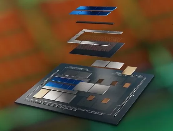
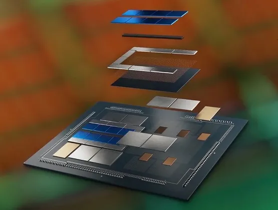
Throughout the current millennium, System-on-Chip (SoC) has been the gold standard for optimizing performance and cost of complete electronic systems. By incorporating practically all the phone’s digital plus analog capabilities onto a single, giant chip, the mobile phone processor serves as a near-perfect exemplar of SoC. But today’s leading integrated circuits (IC) are pushing up against the upper limit of a chip’s size which is limited by the manufacturing equipment’s optical reticle size. This has proven difficult to increase and has grown only slowly over the years. Yet market pressure continues unabated for bigger, more capable electronic systems with more integrated memory, more digital logic, and more analog/mixed signal circuitry. An emerging solution to this tension is 3D and 2.5D multi-die chip assemblies – often referred to as 3D-IC. The key technology breakthrough of 3D-IC is that it makes it possible to spread a system out over multiple, smaller chips that are then assembled close together and interconnected with high-speed, low-power interconnect technologies. By abandoning the need to integrate an entire system on a single SoC and instead allowing it to be disaggregated over multiple chips, 3D-IC enables Moore’s Law to break through the reticle size barrier, improves yield by shrinking the size of individual chips, and makes it possible to mix different process technologies optimized for each function. The Four Engines Driving Semiconductor Design The road forward is not without its challenges, however, and we are seeing design companies making significant efforts to adapt and come to grips with the following four technology and market drivers: The requirement for concurrent multiphysics analysis to ensure reliable and efficient electronic systems The blurring of the lines between silicon and system The need for open and inclusive multiphysics platforms that interoperate with the multitude of design platforms The need for, and value of, bespoke silicon for hyperscalers and system companies Blurring of Silicon and System Design The advent of 3D-IC opens up new horizons for solutions that can be implemented in silicon. But it also forces a closer integration between two distinct technology markets that have co-existed symbiotically for many decades: IC design and printed circuit board (PCB) design. These markets use different tools, different data formats, different manufacturing back-ends, operate at different computational and geometric scales, and focus on different physical concerns. Yet, 3D-ICs share many aspects of both markets: They include monolithic chips but also board-like substrates to stitch the chips together. And in between the two disciplines is packaging, a completely different domain that is requiring companies to re-imagine their design capabilities and flows, as well as their organizational structure. Open, Extensible Multiphysics Platforms The siloed isolation of chip design from PCB design and package design means that each of these markets has developed insular data structures that are ill-suited to deal with the breadth of multiphysics analysis for 3D-IC design. Many different physical disciplines, including computational fluid dynamics, mechanical stress, and electromagnetic radiation, all need to work together based on open and extensible multiphysics platforms. These platforms must embrace the modern cloud compute paradigm and enable an ecosystem by allowing individual design platforms to connect for comprehensive multiphysics analysis. Bespoke Chips Today’s market-leading companies are heavily dependent on technology for their continued success and market differentiation. Everybody from online retailers to telecommunications to social networking companies and hyperscalers are moving away from off-the-shelf solutions and turning to custom-built silicon to give them an edge. Many of these companies are seeking to gain market share by leveraging proprietary AI/ML algorithms trained on their extensive troves of market data – but this requires huge amounts of compute power and specialized chips. Access to high-quality silicon solutions is vital in today’s world and the demand is for continually more complex and powerful electronics. 3D-IC an Inflection Point in Electronic Design To be sure, 3D-IC design is at an inflection point in electronic design and presents major challenges that are realigning the electronic design industry around this new reality. For more insights on this topic from a semiconductor industry leader, please view the Keynote Address 2.5D and 3D – The Road Ahead by Vicki Mitchell, VP Engineering, Arm Central Engineering Systems Group presented at the latest Ansys IDEAS Forum. And for an EDA perspective, please view Successful 2.5D and 3D Multi-die Silicon System Design Using Synopsys’ 3DIC Compiler and Ansys’ Multiphysics Analysis from Synopsys SNUG World 2021. About John Lee John Lee is general manager and vice president of the Ansys Electronics and Semiconductor Business Unit. Lee co-founded and served as CEO of Gear Design Solutions (now Ansys), developer of the first purpose-built big data platform for integrated circuit design. He cofounded two other startups (Mojave Design and Performance Signal Integrity), which successfully exited into companies now part of Synopsys. He holds undergraduate and graduate degrees from Carnegie Mellon University.
Read More
As monolithic scaling slows down, the semiconductor industry is increasingly relying on advanced packaging technologies to extend Moore’s law through heterogeneous integration. Higher on-package bandwidth, improved yield resiliency and the need to integrate diverse IP from multiple foundries are driving demand for advanced packaging technologies that address these issues but introduce challenges of their own such as efficient power delivery to all the different domains in a heterogeneous system. SEMI spoke with Kaladhar Radhakrishnan, Intel Fellow at Intel, about heterogeneous system integration trends and new developments in the semiconductor industry. Radhakrishnan shared his views ahead of his keynote at the SEMI Connecting Heterogeneous Systems Summit, 1-3 September 2021, an online event. Join the summit to meet experts from Intel and other key industry influencers. Registration is open. SEMI: What is driving the adoption of electronics and semiconductor devices nowadays and why is the development of new and innovative technologies important? Radhakrishnan: We are living in an increasingly data-driven world where devices have become an integral part of our lives. A recent study estimated that in the United States alone, 13.6 connected devices per capita consume an average of 300 gigabytes worth of data every month. In the workplace, COVID-19 has driven fundamental business changes that has sped up the adoption of digital technologies such as virtual conferencing, remote work, and e-commerce. Organizations are realizing that a high-quality video conference can be an adequate substitute for many in-person meetings. As a result, businesses are accelerating the digital transformation in order to adapt and thrive in this new environment. Five decades of sustained exponential growth in semiconductor performance has conditioned the average digital consumer to expect more from their devices. However, there are some headwinds ahead as traditional scaling slows down and power density rises. Because consumers and businesses are now generating data at a faster rate than they can consume it, technologists need to scale compute, storage, and bandwidth even faster to keep pace. Without investments in research and development of new and innovative technologies to address these challenges, the full potential of this data will go unrealized. SEMI: What forces are heightening the importance of heterogeneous system integration? What are the implications for increased on-package bandwidth, improved yield resiliency and the need to integrate diverse IP from multiple foundries? Radhakrishnan: The semiconductor industry increased transistor density and scaled performance through classical Dennard scaling until the turn of the century. By then, the gate oxide thickness had scaled down to atomic dimensions and the exponential increase in sub-threshold leakage signaled the end of scaling through traditional methods. Since that time, the chip industry has been relying on innovations in transistor materials and structures such as high-k metal gate, strained silicon, and FinFETs to keep pace with Moore’s law. However, this alone will not be sufficient to continue scaling and the industry needs to explore other vectors to augment improvements in transistor technology. Heterogeneous integration through advanced packaging is one key technology that can help drive these gains. Technologies like Foveros can enable device density scaling by creating a 3D stack of multiple die using high-density interconnects. Heterogeneous integration enables chipmakers to move from a monolithic system designed on a single large chip to a heterogeneous system comprised of a number of smaller chiplets. The main benefit of using smaller chiplets is that they improve yield and enable application based customization of the foundry processes. However, if the disaggregation to smaller chiplets is not accompanied by an increase in on-package bandwidth, the power and performance penalties associated with chiplet-to-chiplet communication will hobble system performance. This is why advanced packaging technologies that improve die-to-die communication are key enablers for heterogeneous integration. SEMI: What are some of the key technology challenges in developing heterogeneous systems? Radhakrishnan: The obvious challenge that most people focus on is the need for improved on-package bandwidth. However, as we rely on 3D stacking to continue device scaling at the package level, it is important to comprehend power delivery and thermal challenges as well. Power to the top die has to be delivered through TSVs on the bottom die, which not only adds resistance but also reduces the useful area available on the bottom die. This problem is further exacerbated when we stack more than two die. Excessive noise on the power delivery network can cause timing issues that limit the maximum operating frequency of the transistor. Similarly, when we stack multiple die, we must take into account associated thermal challenges. For example, each interface of the multi-die stack adds thermal resistance, which makes it harder to cool the chips at the bottom. SEMI: What are some of the key global market trends that driving demand for heterogeneous and system-level integration? Radhakrishnan: The number of artificial intelligence (AI) and machine learning applications have grown dramatically due to their ability to solve highly complex problems across a wide range of segments. AI and machine learning models require more memory bandwidth and compute capabilities that are difficult to achieve without some form of heterogeneous integration. Another market trend driving demand for heterogeneous integration is the increasing reliance on custom hardware accelerators. To combat the slowdown in frequency scaling and single-core performance, we have moved to multi-core architectures by tackling the inherent parallelism in our workloads. However, Amdahl’s law tells us that such an approach will hit a bottleneck when we reach the limits of the serial portion of the workload. As these constraints slow the performance of general-purpose processors, the reliance on custom hardware accelerators to boost performance for specific workloads is growing. Heterogeneous integration at the system level with a combination of CPUs, GPUs, FPGAs and other accelerators can optimize system power and performance. SEMI: What solutions is Intel developing to address these market needs? Radhakrishnan: Intel is actively involved in the development of the industry ecosystem for heterogeneous integration. We have developed a number of innovative advanced packaging solutions such as the EMIB and Foveros that are used in products today. Intel is also developing the next generation of advanced packaging technologies, Foveros Omni and Foveros Direct, which will dramatically scale the IO density by using direct Cu-Cu bonding technology. Foveros Omni is a crucial building block technology to enable high-voltage power conversion on the package for efficient power delivery. Intel is uniquely positioned to predict the design needs for future systems and deploy its resources to develop the technology building blocks needed to continue performance scaling. Our IDM 2.0 strategy enables us to leverage our leadership in packaging technologies to design the best products and use the best IP to deliver leading products across a broad range of categories. SEMI: What do you expect from your participation at SEMI Connecting Heterogeneous Systems Summit? Radhakrishnan: I’m hoping to shed some light on some of the new technologies we have been developing at Intel to enable heterogeneous system integration. I also want to bring awareness to the power-related challenges we are facing with heterogeneous systems. I also look forward to listening to what other industry leaders have to say on the topic. Kaladhar Radhakrishnan is an Intel Fellow and a Power Delivery Architect with the Technology Development group at Intel. He plays a significant role in shaping and driving power delivery technologies for Intel microprocessors. His areas of expertise include integrated voltage regulators, advanced packaging and passives technologies. Kaladhar is a two-time recipient of the Intel Achievement Award, the highest Intel honor an individual or small team can receive. He has authored four book chapters, over 40 technical papers in peer-reviewed journals, and has been awarded 35 U.S. patents. He has also served as an adjunct professor at Arizona State University. Kaladhar joined Intel in 2000 soon after receiving his Ph.D. in Electrical Engineering from the University of Illinois at Urbana-Champaign. Serena Brischetto is senior manager of marketing and communications at SEMI Europe.
Read More
In the span of a few short months earlier this year, Mentor Graphics became Siemens EDA and introduced a suite of integrated hardware-assisted verification tools, the first product launch under the new Siemens EDA brand. Jean-Marie Brunet, senior director of marketing, product management and product engineering at Siemens EDA, orchestrated the launch and connected with me for a discussion about the chip design verification space. As he pointed out, verification and validation of systems is a fast-growing and important market segment to the electronic system design ecosystem. Smith: What trends do you see in chip design? What is driving these trends? Brunet: Chip verification costs continue to grow faster than design costs because of factors such as increasing design complexity, rising computing power, surging I/O traffic activity, increasing energy consumption and the widespread use of peripherals. These dynamics are being driven by new data center networking, communications/5G, autonomous driving, artificial intelligence (AI) and machine learning (ML), and storage applications. These trends also indicate the need for more powerful verification tools and expanded verification objectives that include power and performance analysis. Hardware-assisted verification tools are perfect for meeting these demands. Smith: Chip design verification consumes the most time in a project cycle. Why is this so? Brunet: The verification of designs reaching multi-billion gates and supported by voluminous software stacks is fraught with challenges. To exhaustively check every possible state in a billion-gate design with simulation alone would require up to trillions of verification cycles. That’s why hardware-assisted verification is one of the fastest-growing technologies in EDA. Given the complexity of today’s SoC design, it’s no surprise that verification is the largest undertaking in the entire project design cycle, consuming more than 50% of it. It also has the greatest impact on quality, cost and schedule because it prevents designs from failing at first silicon. While a respin of a large design taped out at a node below 10 nanometers could cost more than $10 million, delaying delivery of a new product for a few months in a highly competitive market may cost hundreds of millions of dollars. Smith: What other challenges do engineers face trying to verify a chip design will work as intended? Brunet: Verifying an SoC design is a massive undertaking and, in parallel, verification teams are trying to streamline and optimize verification cycles. SoC design groups are tasked with completing full system-level verification prior to creating production masks by thoroughly vetting all hardware blocks, interactions between those blocks, and the software developed for the end application before the chip is built. To alleviate this enormous pressure, they are starting to adopt a shift-left methodology for early functional verification as soon as individual blocks of a SoC design become available. It helps jump-start embedded software validation before full system validation is completed to save time and allow engineers to work in parallel, not serially. While it is an effective approach, it creates the need for a complete and integrated suite of hardware-assisted verification tools to verify and validate a design’s hardware and software components. Smith: How do you define hardware-assisted verification and how does it help solve these challenges? Brunet: A typical definition of hardware-assisted verification is special purpose hardware to accelerate verification. In other words, hardware emulation and FPGA prototyping. Hardware-assisted verification is a mandatory investment as single-die or multi-die chips get larger with more complexity and more interfaces, making hardware and software code integration critical early in the design cycle. Because software performance defines a chip’s success, the need to perform software workload-based analysis is acute, not just analysis of chip functionality, but also accurate performance and power consumption in the context of real-world applications. Hardware-assisted verification is the only option when hardware and software meet. By combining emulation, desktop FPGA prototyping boards and enterprise FPGA prototyping platforms to work on the same SoC design, a verification group can assemble a complete hardware-assisted verification system for thorough and exhaustive verification and validation. Smith: Where are the big opportunities for hardware-assisted verification? Brunet: New end-user applications are coming from computing and storage, AI/ML, 5G, networking and automotive. Recently released market data from the ESD Alliance shows that in 2020, hardware-assisted verification revenues exceeded $700 million. It is reasonable to assume that revenues of $1 billion will be within reach in the next few years given the amount of chip design activity at advanced nodes below 10nm. Smith: With the design/verification and manufacturing phases of the semiconductor supply chain more closely aligning, what role does hardware-assisted verification play? Brunet: Semiconductor manufacturing and the supply chain that supports it benefits greatly from the continued innovation in verification and validation tools and methodologies. With this innovation, designs are delivered to the manufacturing flow with a much greater chance of passing first silicon with success. This reduces friction in the semiconductor supply chain since IP and chips are available when anticipated. Hardware-assisted verification is a quick-moving, highly leveraged resource that helps a design and verification team to ensure chips are manufacturable and meet the functionality, power and performance requirements for the end-product application. Jean-Marie Brunet is the senior director of product management and engineering for the Scalable Verification Solutions Division at Siemens EDA. He has served for over 20 years in application engineering, marketing, and management roles in the EDA industry, and has held IC design and design management positions at STMicroelectronics, Cadence, and Micron, among other companies. Jean-Marie holds a Master's degree in Electrical Engineering from I.S.E.N Electronic Engineering School in Lille, France. Jean-Marie Brunet can be reached at [email protected]. About Bob Smith Robert (Bob) Smith is executive director of the ESD Alliance, a SEMI Technology Community. He is responsible for the management and operations of the ESD Alliance, an international association of companies providing goods and services throughout the semiconductor design ecosystem.
Read More
Over the past 50 years, the field of engineering simulation has developed numerical methods that enable engineers to solve 3D physics problems faster, easier, with greater accuracy and more robust results. Finite element analysis (FEA), finite volume methods (FVM) and finite different time domain (FDTD) have increased solver efficiency while dynamic visualization techniques improve what is often called user-friendliness. Despite these improvements, certain challenges still remain. Specifically, simulation requires the simultaneous trade-off of: Accuracy of results Speed of results Ease of use of the workflow Robustness of the workflow Take, for example, mesh generation, the building block of multiphysics solutions. It is well known that using coarser meshes increases simulation speed but will result in loss of accuracy. Similarly, easy-to-use workflows with simpler meshes also reduce accuracy, and can introduce other issues: The simulation may not converge and the robustness fails. Ansys is exploring the use of AI/ML to solve all of these problems. Simultaneous Improvements Commercialization of AI began in the 1970s, but the field actually got its start a decade earlier with the development of rules-based expert systems. The simplest form of AI, these systems rely on curated human expertise to solve problems that would normally require human intelligence. We’d expect that AI/ML applications would be actively used in science and medicine, from streamlining drug discovery and advancing robot-assisted surgery to automating medical records that can be instantaneously accessed by providers anywhere in the world. But AI/ML is rapidly being successfully adopted by an increasingly broad range of industries and users. It’s helping consumer brands mine their social media to find out customers’ feel about their products (sentiment analysis), giving investors a leg up on stock trade opportunities (financial algorithmic trading) and enabling e-commerce owners to personalize offerings to online shoppers (recommendation engines). At Ansys, we can use AI/ML methods to automatically find the parameters of simulation to simultaneously improve speed and accuracy. We believe applying AI/ML will enable us to: Further improve customer productivity Augment simulation, including accelerating chip thermal solutions and developing a fluids solver that combines high-fidelity solutions in local regions with ML methods in coarse regions Optimize design space exploration Drive business-intelligence decisions such as resource-prediction needs for our solvers Combine data analytics-based and simulation-based digital twins to create accurate and fast digital twin hybrids In other words, we believe that AI/ML will help us narrow the gap between the ideal world, where time, effort, efficiency and results are perfectly balanced, and what happens in real life – and make productivity, ease of use, and accuracy a little less of a trade-off. To learn more about applying AI/ML to autonomy, click here. Prith Banerjee is Chief Technical Officer at Ansys, Inc.
Read More
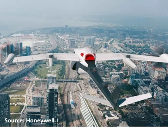
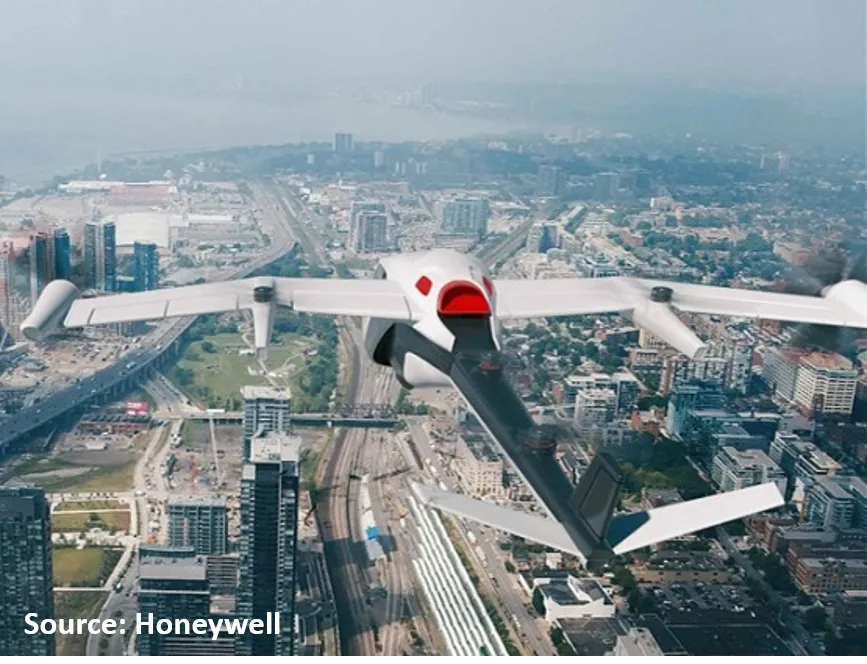
While flying cars have been a science fiction mainstay for decades, new sensors, software and other technology put personal air travel vehicles within reach. MEMS and Sensors Industry Group (MSIG) interviewed Dr. Alberto Speranzon, Fellow at Honeywell Aerospace Advanced Technology, about his upcoming keynote Sensors and Software Enabling Autonomy for Urban Air Mobility at the MEMS and Sensors Technical Congress (MSTC 2021) virtual event, April 13-15. Dr. Speranzon will discuss Honeywell’s challenges in enabling air taxis and the path forward to building out the necessary infrastructure. SEMI: People have dreamed of flying cars for decades. What has changed recently that makes them a near-term reality? Speranzon: There certainly are multiple factors that have contributed to pushing both new startups and established aerospace companies to make this dream a reality. Advances in battery technology are bringing electric aviation closer to being viable. There is still more to be done to achieve higher energy density in batteries, but already with today’s technology we can have vehicles that can fly from the suburbs to the downtown of a large U.S. city. At the same time, urbanization has created a lot of congestion, so finding new, efficient ways to move people and goods across megacities is becoming a critical need. Undeniably, the autonomous car industry has contributed to demonstrating that it is possible to achieve levels of automation and autonomy that were unimaginable just a few decades ago. The advances in sensing and computation required to make self-driving cars a reality is certainly going to help the aviation industry to develop autonomy in the air. SEMI: An air taxi must be highly sensorized. What types of sensors pose your biggest development challenge? Speranzon: Aircraft based on today’s battery systems simply cannot accommodate the size, power requirements and weight of sensors used by standard airliners. So there still is work to be done to reduce the SWaP (Size, Weight and Power) of these systems. Honeywell, for example, has developed a multipurpose radar, the IntuVue RDR-84K, that is only about the size of a paperback book. It can detect traffic, terrain and even weather, and was specially designed for air taxis and cargo UAS (unmanned aerial systems). Today, however, we still rely on human pilots to make the very complex decisions and, despite all the limitations that human eyes have, we do rely on them in a multitude of complex situations. There is also growing interest in integrating cameras into autonomous air taxis and similar platforms. Cameras can’t work alone, because they are affected by foggy, rainy and dim conditions. But they are lightweight, inexpensive, and require little power. That can make them very useful when combined with a compatible radar system like the RDR-84K. While these sensors bring new opportunities to the aerospace industry, they also pose some big challenges. For example, today’s state-of-the-art algorithms for image processing are machine learning algorithms called deep neural networks. They’re capable of extracting high-level information from pixels. But when it comes to aircraft certification, these algorithms face major hurdles. There is no software of this kind in any certified air vehicle, and it is unclear how regulators would certify neural network-based software components. Developers could avoid these new machine-learning algorithms and use standard computer vision methods instead. But they still face the challenge of deciding the type and quantities of images sufficient to declare the software “bug-free.” A similar set of questions will be also be true for radars, as they will be used to feed data more directly into the autonomy modules of future air taxis. So in the short term, we need to tackle the challenge of reducing the size and weight of sensors. But in parallel, we need to develop new ways to take advantage of machine learning: utilizing cameras and radars for autonomous decision making while still ensuring the highest standards of safety. SEMI: How is autonomous air mobility more or less challenging than autonomous ground vehicles? Speranzon: They are both challenging in their own ways. Autonomy on the ground – and I am thinking specifically of autonomous cars – is challenging as their “normal” behavior is very complex. We humans can drive from point A to point B over the public road network without a second thought. But to a machine, the heterogeneity of the people driving on the road, their sometimes unpredictable behavior, the changing weather conditions and shifting environments pose huge challenges. These things make what we call “normal driving” a very difficult problem to solve. At the same time, however, “off-nominal” scenarios in ground autonomy, while complex, are not orders of magnitude more complex than “nominal” scenarios. Ground vehicles can brake and stop, change lanes or move to the side of the road to avoid a crash or manage a malfunction. For autonomous air vehicles, the difference between nominal and off-nominal scenarios is more extreme. “Nominal” flying can rely on some of the existing aviation infrastructure, like communication between air traffic control and other aircraft. Air taxis can follow predefined paths and long-established aviation procedures as they move from vertiport A to vertiport B. This results in more automation than autonomy: everything is prescribed in advance and the onboard computer will follow what is pre-defined. Thus, nominal conditions will be fairly simple. However, in case of accidents or emergencies, aircraft face situations that are orders of magnitude more complex than nominal scenarios. An air vehicle cannot easily just “stop.” It could be 1,000-2,000 ft above ground, possibly above a bustling city. Human pilots go through rigorous training to be able to deal with emergencies like these. Consider the split-second judgments and airmanship behind the 2009 “miracle on the Hudson” landing. Asking autonomy to make the right decisions and execute emergency behaviors is a huge challenge. And these systems will need to be certified to the aviation industry’s very high standards. At present, we do not even have a well-established set of certification rules that an autonomous flying vehicle should comply with. SEMI: How soon might I be able to take an air taxi ride? Speranzon: Initial deployment of air taxis will happen around 2025. They will have human pilots but will use simpler interfaces than today’s cockpits. This first step will provide technologies that make it easier to take off and land, and to avoid traffic. That will reduce the need for highly experienced pilots and should help alleviate the overall shortage of pilots in the aviation industry. Fully autonomous air taxis are likely not going to show up until after 2030. In the beginning, they will likely fly only in regions where the weather is good most of the time. The autonomous car industry has already adopted this strategy, mostly deploying their technology in regions where the weather is dry and sunny. Soon, however, we’ll start seeing operations in “all-weather” scenarios and an increasing number of air vehicles within the same airspace. There is one critical stepping stone on the way to fully autonomous passenger aircraft: the success of fully autonomous cargo drones. For light parcels we will see initial deployments in 2022 or 2023, followed by larger UAS capable of transporting heaver cargo in 2024-2025. But whatever the timing, these are very exciting times. The aviation industry is witnessing a revolution with new vehicle manufacturers, new technologies and, likely, new applications we have not even dreamt of yet. Learn more about Honeywell’s work in urban air mobility and unmanned aircraft at aerospace.honeywell.com/uam. Alberto Speranzon is a Fellow within Honeywell Aerospace Advanced Technology. He received a Ph.D. in Electrical Engineering from the Royal Institute of Technology (KTH), Sweden in 2006. Since joining Honeywell, Alberto has been working on various aspects of autonomous systems for urban air mobility, leading such research areas as program manager and principal investigator. He is an IEEE Senior Member and a member of the Board of Governors of the IEEE Control Systems Society. Nishita Rao is product marketing manager at SEMI.
Read More
Ride the Wave of Smarter Manufacturing The year 2020 sparked a tremendous acceleration in the digital transformation worldwide, driving a sharp rise in demand for semiconductors and escalating pressure on chip factories to reduce manual functions on the shop floor. The mindset of the semiconductor industry saw a remarkable shift as it recognized with heightened urgency the need to deploy data-driven visualization, analysis, scheduling and dispatching solutions to increase automation to improve production speed and efficiency. Amidst the new excitement around Industry 4.0, chip manufacturers are rapidly deploying new technologies including IIoT, big data, machine learning and Autonomous Intelligent Vehicles (AIVs). Yet for many chip manufacturers, the path to building a smart factory is far from clear because they lack an overall digital transformation strategy. Smart manufacturing is a broad concept covering an array of technologies and solutions, making a holistic, mid- to long-term digitalization strategy rooted in the overall business strategy crucial. There are no shortcuts that can move a manufacturer instantly to Industry 4.0. Instead, this transformation is a step-by-step undertaking with a natural evolution. Some Factory Tasks Must Remain Manual – For Now The semiconductor industry has reached a point where manual processes are no longer efficient enough to support mass chip customization and remote operations. The many technological and standardization advances behind automation can help streamline some of a factory’s most labor-intensive tasks including the loading or unloading of machines or lot tracking and data collection while reducing operational costs. Still, some tasks remain very difficult to automate. For example, handling errors and exceptions presents the greatest challenge since some errors are hard to anticipate. What’s more, the cost of automating error handling can be prohibitive. Eliminating Gaps in Connectivity Often, critical data sources aren’t available due to lack of equipment integration, incomplete product quality monitoring or gaps in material tracking. Closing these gaps in connectivity enables the collection of data and provides rich, reliable information for analysis and reporting that can drive continuous operational improvements, optimizations and efficiencies throughout a factory. But keep in mind that data integration alone can be a challenging task. The selection and proper enrichment of relevant data is, in many cases, not just a technical problem but requires a detailed and in-depth knowledge of the manufacturing steps to be analyzed and optimized. Even when data is available, it might be still difficult to make decisions or implement improvements if it is in siloed systems that require manual processes to integrate and translate into useful information. Problem solving at this level is possible but extremely time-consuming. Manual integration is not only ineffective but costly, draining time, human resources and money from the factory. The right contextual information for the data is vital to unleash its potential and make improvements possible. Dispersed solutions cannot control processes because they span functional areas and people, physical and business entities. Backbone software for shop-floor operations that controls all other applications is central to smart manufacturing. Data-Driven Manufacturing The semiconductor industry is expert in data collection and leads many other industries in this area. The problem is often that chip companies use only a fraction of the information they collect for the analysis and insights needed to improve operational efficiency. By comprehensively integrating all distributed data into a single version of truth – in one location where it is always available – companies can make data analysis and problem solving almost frictionless. Keep in mind that data platforms and edge solutions, within the context of manufacturing, will not be adopted as part of a greenfield initiative. Building a solid automation architecture is only feasible and beneficial by deploying new technologies such as machine learning and artificial intelligence (AI). Analysis of historical data provides important context and reveals deviations such as unexpected process time, uncommon material accumulations or issues with material transport. By integrating swift control actions for new data point collected, manufacturing operations can shift from reactive problem-solving to proactive analysis and operational improvements. The tremendous increase in interest and investment in AI for manufacturing automation only became possible with the availability of low-cost sensors that generate huge volumes of data and solutions for storing and processing that at low cost. AI and other leading-edge technologies transform the tedious but critical process of extracting insights from data, making it instantaneous, streamlined and achievable for every manufacturer. The maturity of smart manufacturing hinges on the extent to which a factory is data-driven. This requires foundational investments to improve traceability, connectivity and real-time operations – and finally making sure that data helps us what to do and when to do it. Ricco WALTER is managing director of SYSTEMA Automation in Singapore.
Read More