downloadGroupGroupnoun_press release_995423_000000 copyGroupnoun_Feed_96767_000000Group 19noun_pictures_1817522_000000Member company iconResource item iconStore item iconGroup 19Group 19noun_Photo_2085192_000000 Copynoun_presentation_2096081_000000Group 19Group Copy 7noun_webinar_692730_000000Path
Skip to main content
Default Banner Image

TEL

As the world combats climate change, the chip industry continues to build momentum in becoming a better steward of the environment. In July, Taiwan chip giant TSMC became the world’s first semiconductor company to join RE100, the global initiative to move away from a widespread reliance on fossil fuels and toward 100% renewable electricity. Applied Materials soon followed with a commitment to expand its renewable energy capacity. For the past four years, ASE Group, the largest outsourced semiconductor assembly and test (OSAT) provider, was named an industry leader in the Dow Jones Sustainability Indices (DJSI), making clear its commitment to protecting the environment. For its part, TEL was selected to be part of the FTSE4Good, a series of ethical investment stock market indices, and FTSE Blossom Japan, an index that gauges the performance of Japanese companies demonstrating strong Environmental, Social and Governance (ESG) practices.SEMI bolsters commitment to green energySEMI has also strengthened its commitment to promoting renewable energy in the semiconductor industry by adding the Green Power Pavilion at this year’s SEMICON Taiwan and continues to support the green energy movement as a co-organizer of Energy Taiwan. The largest renewable energy event in Taiwan, Energy Taiwan features international exhibitions, forums, policy initiatives and business matching events. This year the event attracted more than 12,000 visitors from 50 countries to highlight renewable energy breakthroughs and new products. The SEMI events complement RE100, which works across a wide range of industries that include financial services and retail. The initiative connects more than 260 members that count among them the world’s most influential businesses such as Apple, Google and Facebook and their suppliers through educational events.In many respects, TSMC is becoming a beacon of green energy in the chip industry. In July, the company committed to 20-year agreement to buy offshore wind power gear made by energy firm Ørsted in Taiwan, the global leader in the wind power industry. According to the purchase agreement, TSMC will offtake full production from 920-megawatt wind farms off the coast of Changhua County in western Taiwan expected to start operations in 2025 or 2026. The agreement will by far mark the world’s largest corporate green energy order in the semiconductor manufacturing and renewable energy industries and demonstrates TSMC’s long-term commitment to environmental sustainability.In addition to sourcing renewable energy, TSMC has been working closely with its downstream and upstream suppliers to help drive supply chain improvements geared toward a greener industry by offering on-site coaching, energy audits and educational resources. But the company's focus on energy efficiency is nothing new. For years, its Supply Chain Management forum has promoted industry sustainability and corporate responsibility. Moreover, TSMC worked with SEMI at this year’s SEMICON Taiwan to generate greater awareness of the importance of green energy to the industry and encourage SEMI members to become more involved in the movement.Supply chains expand eco-friendly practicesThe drive toward greener semiconductor manufacturing is also expanding to encompass entire supply chains. One notable initiative is Green Supply Chain Management (GrSCM), an effort to integrate environmental thinking into every level of the supply chain, from product concept to distribution. GrSCM involves the retooling of product design, materials sourcing, manufacturing and processes to reduce the ecological footprint of factories. So far, the results are encouraging. More companies are factoring environmental sustainability into their purchasing decisions to urge suppliers to better manage their power usage and join the green energy movement – an important step in curbing the unavoidable consequences of climate change. Terry Tsao is Global Chief Marketing Officer at SEMI and President of SEMI Taiwan.
Read More
Like so much else these days, career mentoring in the semiconductor industry has gone virtual. And, among hiring managers, for good reason: Chip companies are facing a new urgency to hire skilled workers as recent SEMI forecasts spanning packaging materials and fab equipment spending show strong growth in 2021 – a trajectory that puts even more pressure on an industry confronted with a worker shortage to attract and recruit new talent.Enter SEMI Korea, which early this month gathered nearly 4,000 sheltered-in-place South Korea university students to offer tips from semiconductor industry insiders on how to kick-start their careers in the chip business. In 14 sessions over three days, industry powerhouses offered guidance across topics ranging from educational preparation and job skills to resume writing and interviewing. Like last year’s on-site event, students from Seoul accounted for the bulk of those online for Campus Outreach On-Air. But this year saw a far higher turnout of students in provincial cities thanks to the ease and convenience of virtual communications – a silver lining in the age of COVID-19.Establishing a successful career in the semiconductor industry starts with a mix of soft and hard skills, according to Changjin Kang, CEO of SEMES, one of the top 10 global semiconductor equipment companies. Keynoting the event, Kang pointed to six key attributes in particular – caring, resilience, execution, analysis, tenacity and experience – under the acronym C.R.E.A.T.E.Caring means empathy for colleagues, understanding their unique work environment and challenges, and building strong relationships. To help cope with the stress that can come with working in the industry, workers must be also be resilient by managing the emotional demands of a job and getting enough rest. Execution comes down to thorough, methodical planning. Carefully analyzing information to make data-driven decisions is a critical aspect of successful outcomes, while having the tenacity to push through difficult technical challenges helps engineers develop the right solutions. And getting out from behind the desk to learn from colleagues is important in building experience.Human resources representatives and engineers from Applied Materials, ASML, Dongjin Semichem, EO Technics, Jusung Engineering, KLA, Lam Research, Merck KGaA, Darmstadt, Germany, PSK, SEMES, SK Siltron, TEL and Wonik IPS shared with the students the key competencies needed to forge a career in the semiconductor industry. Engineers pointed to the benefits of improving their English skills through language training and continuing their education by pursuing engineering certificates. Human resources representatives stressed the importance of a global mindset since, as part of the global semiconductor ecosystem, engineers and other staff often communicate via conference calls with colleagues around the world.In a post-event survey, the students – all digital natives – awarded the event 4.3 out of 5 points for overall satisfaction and made clear that they prefer online Campus Outreach to the on-site event.“Thanks to SEMI and the companies for providing a great opportunity to meet experts and HR managers,” one student pointed out in the survey. “It was very useful because it opened up opportunities for many students to communicate with semiconductor companies.”“It was nice to know what works semiconductor engineers do,” said another, “and how as university students they prepared for employment.”SEMI Korea thanks the nine semiconductor companies that sponsored Campus Outreach On-Air to help build the industry’s talent pipeline and the students for their invaluable participation.Jaegwan Shim is a marketing specialist at SEMI Korea.
Read More
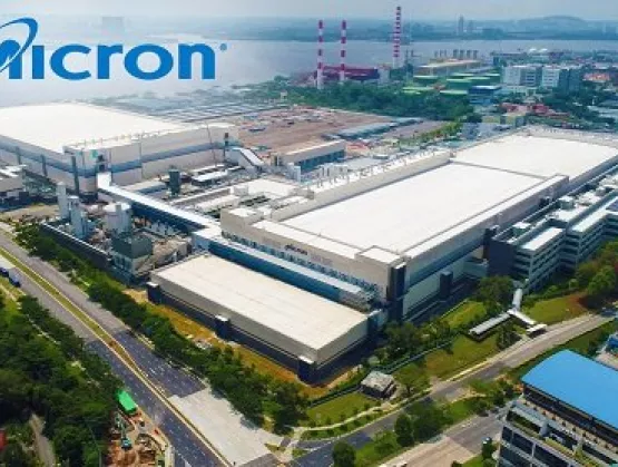
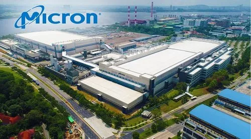
Making Strides TogetherKnowledge is power – especially when it is shared. This principle formed the foundation for Micron’s Go and See virtual visit of its Singapore manufacturing plant on 26 August 2020 as 27 companies including GLOBALFOUNDRIES, ST Microelectronics, Infineon, TEL, ViTrox , IBM, HP and UTAC joined the first-of-a-kind virtual factory visit. The chip industry powerhouses gathered to see how Micron’s Lighthouse frontend wafer fabrication facility leverages Fourth Industrial Revolution technologies to drive new production and cost efficiencies.They saw clear markers of a transformed organisation and spoke with working-level staff, managers and front-line employees. Company representatives also met virtually with Micron management teams from organisations that led its digital transformation – from pilot programs to integration at scale – to realise significant financial and operational benefits. The mix of technologies they deployed to make it all happen included artificial intelligence (AI), big data analytics and the Industrial Internet-of-Things (IIoT).Micron’s Singapore-based fab facility earned Lighthouse certification earlier this year from the World Economic Forum’s Global Lighthouse Network. The Go and See tour was co-sponsored by SEMI Southeast Asia and McKinsey Company.Transformation is CrucialBy embracing Lighthouse principles, semiconductor sectors and companies can accelerate their digital transformation to boost operational and financial efficiency while helping increase productivity across the electronics supply chain. It will take time for Southeast Asia semiconductor manufacturers to transform to digital operations, though we’re seeing growing interest in Industry 4.0 practices as they begin to understand that the deployment of new technologies and applications will help them better understand real-world benefits of smart manufacturing use cases and solutions. SEMI believes shining the spotlight on companies like Micron can illuminate the way forward for other companies to help drive the industry’s digital transformation. We look forward to seeing companies build on this momentum as they start to leverage leading-edge technologies to improve efficiencies and promote sustainability.Bee Bee Ng is president of SEMI Southeast Asia.
Read More
Would you buy your next hotdog in parts, from un-coordinated suppliers? For example: Get the bun from a baker, the sausage from a butcher, mustard and/or ketchup and veggies from the nearest supermarket? If yes, you may find the sausage being too small, the veggies too big for the bun, and, when you finally finished adding mustard/ketchup and start eating, you may “enjoy” a cold sausage on a soggy bun!This “hotdog example” is just a very simple way to highlight the advantages of a well-coordinated semiconductor supply chain. What may be a few dollars and cents wasted in this hotdog purchase, can become millions of dollars lost to delays and inefficiencies during the roll-out of a new electronic system.Complexity is Increasing the ChallengeThe very innovative semiconductor industry is continuing to develop more complete and complex building blocks for electronic system solutions, with the intent of making our customers’ lives easier. However, every new technology takes increasingly more time for technical and business interfaces to mature before all the semiconductor supply chain members can serve customers in a smooth, efficient and cost-effective manner. In particular, coordination between design and manufacturing has always turned out to be in the critical path.SEMI, the manufacturers’ trade organization, and the Electronic System Design (ESD) Alliance, representing electronic design automation (EDA) tools vendors, developers of intellectual property (IP = ready-made building blocks for ICs) and IC design service providers, both recognized these challenges. Late in 2018, these two industry organizations decided to jointly address this painful, costly and often a very frustrating, yet critical path and became Strategic Association Partners, The goal is to establish a well-coordinated semiconductor supply chain.To make the value propositions of this partnership highly visible and demonstrate the first joint accomplishments, SEMI’s well-known SEMICON West conference and, in its first year, ES Design West, will be conveniently co-located in San Francisco’s Moscone Center from July 9 to 11, 2019. The synchronized schedules and geographic proximity of these events not only outlines the multi-faceted interdependence of manufacturing and design but encourages and enables conference attendees to do, what previously would have been viewed as “forming cross-border relationships.” It’s a new word now — please join the path to success and expand your network!Navigating SEMICON West and ES Design WestJust in case you are not yet planning to come to San Francisco early July, please check the Agendas-at-a-Glance for SEMICON West and ES Design West, to see how broad and valuable these parallel conferences are for your business. In addition, every customer, partner and semiconductor industry supplier can, from July 9 –11, walk from one conference section to the other, arrange face-to-face meetings, in dedicated meeting rooms, with representatives from both camps and discuss, from the first project planning step to the final production ramp-up, the many topics that need to be coordinated across parts or the entire supply chain to minimize delays and/or cost over-runs.Who Will Lead the Discussions?Conference attendees can, in addition to meeting many important supply chain partners face-to-face, hear about the latest technologies and market trends from key executives in our industry. Featured speakers are: David Pellerin, Head of Global Business Development, Amazon Web Services Lisa Su, President, and CEO, AMD Gary Dickerson, President, and CEO, Applied Materials Laurent Le Faucheur, Principal Engineer, Digital Signal Processing and Machine Learning, Arm, Ltd. Renee St. Amant, Ph.D., Research Engineer in Emerging Technologies and US Innovator of the Year, ARM Dean Kamen, President DEKA Research Development, Founder First and First Global Jeffrey Welser, Ph.D., Vice President and Lab Director, IBM Research-Almaden Dean Drako, President and CEO, IC Manage, Inc. Oreste Donzella, Sr. VP Chief Marketing Officer, KLA Corporation Prakash Narain, President, and CEO, Real Intent, Inc. Aart de Geus, Chairman, and Co-CEO, Synopsys, Inc. Manish Pandy, Fellow, Synopsys, Inc. Nate Baxter, General Manager, Development and Production Group, TEL US Like in previous years, SEMICON West and ES Design West offer a range of special features, addressing Smart Manufacturing, Smart Transportation, Smart MedTech and Smart Workforce development in dedicated pavilions as well as an AI Design Forum. Also, the many exhibitors from both camps will give conference attendees convenient opportunities to get to know new supply chain partners and/or refresh long-term business relationships. Search for the exhibitors you want to meet early July here. Questions to Ask for a Well-Coordinated Semiconductor Supply ChainIf I may, I would like to ask my many friends in the manufacturing camp to spend some time in the ES Design West section and ask the exhibitors a few questions, like: What can you do to get me to profit faster? To reduce development and unit cost? To improve yield, product quality, and reliability? When can you visit my team to discuss how your company can contribute to our goals?Vice versa, I would like to encourage my friends in the design camp to spend time in the SEMICON West section and ask exhibitors what their companies offer. When talking to manufacturers of IC, passive components or circuit boards, assembly and test houses, please ask very specific questions like: How can we help you reduce iterations between you and your customers? How can we help to improve IC test programs? How can we increase the throughput of your manufacturing equipment? How can we apply machine learning (ML) and Artificial Intelligence (AI) to minimize equipment downtime, improve yields and/or shorten production ramp-up?I can assure you that you’ll not only win great friends “across the border” but will be very impressed by the expertise you’ll find in the other camp and the willingness for and benefits of cross-border cooperation.I look forward to meeting you at SEMICON West and ES Design West. Also, if your schedule allows, mark your calendars for the June 12 MEPTEC Luncheon at SEMI in Milpitas, June 18 for the GSA’s Silicon Summit in Santa Clara and June 25 to 27 for the IMAPS SiP Conference in Monterey, CA. Hope to see you at one or all of these important events!Article originally published in 3D InCites. Herb Reiter is president of eda 2 asic Consulting.
Read More
This year, SEMI ISS covered it all – from a high-level semiconductor market and global geopolitical overview down to the neuro morphic and quantum level. Here are key takeaways from the Day 1 keynote and Economic Trends and Market Perspectives presentations.In the opening keynote, Anne Kelleher from Intel pointed to the huge growth of data, with fabs collecting more than 5 billion sensor data points each day. The challenge, Kelleher noted, is to turn massive amounts of data into valuable information. Moore’s law is not dead. New models of computing benefit still from Moore’s law and advances in Si/CMOS technologies for conventional, deep learning, neuro morphic and quantum computing.With customers expecting continual improvements in applications, the question is whether the chip industry is moving fast enough to meet these expectations, Kelleher said. A broad supply chain, equipment and materials innovations, and attracting the “best of the best” college graduates to fuel innovation is key, she said.In the economic trends session, Nicholas Burns (ambassador ret.) from Harvard University pointed out that we will see a major shift in power. The U.S. will remain the major world power over the next 10 years, but we will see a major shift in power in the next coming decades as the gap with countries like China, Russia and India continues to narrow.Duncan Meldrum from Hilltop Economics said that we are passing the peak growth of economic cycle. He warns that a more likely outlook is that a global growth recession is developing. Although semiconductor MSI growth will see a noticeable slowdown in 2019 and 2020, the semiconductor industry is still healthy over the longer term.Bob Johnson from Gartner sees demand shifting from consumer to commercial applications with higher ROIs and budgets. AI, IoT and 5D are the major enablers. He sees structural changes in the semiconductor industry especially for memory but also for Moore’s law with increasing costs and fewer players.The DRAM markets shows volatility and NAND market may be negative in 2019 but non-memory are expected to accelerate mainly because of increasing content and some price hikes.Overall Gartner expects good long-term growth with a CAGR (2017 to 2022) of 5.1%, outpacing 2011 to 2016 CAGR of 2.6%. After a strong 2018 with 13.4% revenue, he forecasts a slower 2019 with 2.6% growth followed by a 8% growth in 2020 and negative growth rate in 2021.Andrea Lati of VLSI went “Back to fundamentals” in his presentation about the industry. VLSI sees a downside bias due to slowing global economy, tariffs, and trade wars. Future drivers are data economy, cloud, AI and automotive.As memory leads the 2019 slowdown, analog, power, logic and other sectors remain in positive territory. VLSI lowered its semiconductor equipment forecast for 2018 from 20% (Jan. 2018) to 14% (Dec. 2018) but increased its sales outlook from 8% to 15% in 2018. VLSI expects revenue to slow into the first half of 2019 but increase to over 4% in the second half of the year, resulting in total 2019 drop of 2.7%. Semiconductor equipment sales are expected to drop from 14% in 2018 to -10% in 2019.Michael Corbett of Linz Consulting, covering wafer fab materials in the years of 3D scaling, sees these as good times for the industry. His outlook for wafer fab materials is bullish based on strong MSI and because wafer fab materials suppliers are getting bigger because of M As.In the Market Perspective session, Sujeet Chand of Rockwell Automation pointed out that as more and more data is generated, the problem is how to get value of all the data collected. There is a need to create the right architecture for machine learning and AI and big data is increasingly being replaced by contextual/structured data. He expects Industry 4.0 to drive foundries to become smaller, more flexible and more productive.In the Technology and Manufacturing session, Aki Sekiguchi of TEL addressed process challenges in the age of co-optimization. The semiconductor industry continues to expand, driven by massive growth of interconnected devices, with heavy demand for processing power and storage. He expects an exponential increase of data from about 40ZB in 2018 to 50ZB in 2020 to 163 ZB in 2026.Major technologies such as DRAM, 3D NAND and logic are dealing with scaling challenges. The density of DRAM (Mb/chip) is plateauing according to 2015 to 2020 trend data, with DRAM is in need of EUV. Memory capacity demand is leading to increasing layers and higher aspect ratios that is concern for 3D NAND and mainly for plasma etch. With Logic already implementing 3D structures, it appears to be in a solid position. Buddy Nicoson of Micron talked about his 50 years in the industry and looked ahead to the next 50. The anchors – quality, cost, scale and speed – won’t change. It has been a great journey so far with unprecedented opportunities and challenges ahead of us. We are getting into a convergence (specialization, integration) and solution-based phase. We will see some inflection points in the coming years, with the best yet to come.Christian G. Dieseldorff is senior principal analyst in the Industry Research and Analysis group at SEMI in Milpitas, California.
Read More
From measurement equipment and components to medical devices, SEMI will showcase SMART technologies at its Smart Starts Here Pavilion, booth 40761, in the Smart Home section at CES, the world’s largest consumer electronics event. Do you want to discuss new technology directions and the latest developments in sensors, displays and electronics manufacturing? Hear about the new SEMI program that promotes “cool” careers in semiconductor manufacturing? Get the outlook for the manufacturing supply chain in 2019 and beyond?Stop by our booth or connect with any of our co-exhibitors in the Smart Starts Here Pavilion at booth 40731 in the Sands Expo Hall A. Co-exhibitors include:Advantest – A world-class technology company, Advantest is a premier manufacturer of measuring instruments used in the design and production of electronic instruments and systems. The company also focuses on research and development (R D) for emerging markets that benefit from advancements in nanotech and terahertz technologies and has introduced multi-vision metrology scanning electron microscopes essential to photomask manufacturing, as well as a groundbreaking 3D imaging and analysis tool.Altergy – Alertgy’s Glucose Monitor is a biosensor-based wristband device that provides non-invasive, real-time blood glucose monitoring for diabetics. The device gives both patients and healthcare professionals on-demand access to blood glucose levels via a smartphone application. C2MI – C2MI is the largest microelectronic innovation centre in Canada. Offering state-of-the-art equipment dedicated mainly to advanced packaging and microelectromechanical systems (MEMS), the centre hosts more than 250 R D scientists. Collaboration and synergy among our partners promote rapid commercialization of advanced prototypes.CHASM – CHASM Advanced Materials is a leading developer and manufacturer of printed electronics materials and battery materials based on proprietary carbon nanotube and ink/coating technologies.Kent Displays – Kent Displays is a global leader in unique eWriter display technology, with expertise in research, development, roll-to-roll manufacturing, and consumer packaged goods design and assembly using the eWriter technology. Kent displays also commercializes and sells the eWriter technology under its brand Boogie Board in a number of global retail markets. mCube – mCube makes the smallest motion sensors in the world. As a technology leader, mCube aspires to be the enabler for the Internet of Moving Things by putting a MEMS motion sensor on anything that moves. With over 500M units shipped, mCube continues to provide the world’s most advanced inertial sensors.Mitsui Chemical – Mitsui Chemical provides chemicals and gases for solutions in energy, agri-system, medical, IoT, and related fields. Mitsui specializes in advanced materials for automotive, ophthalmic lenses, dental, nonwovens, agrochemicals, and packaging. N5 Sensors – N5 Sensors manufactures chip-scale gas sensors that provides reliable gas detection in small-footprint packages. N5’s patented gas sensor technology represents a new era in low-power, microscale gas and chemical sensing that aims to replace conventional gas sensors. N5 is currently offering sensors and modules for integration. Its platform technology enables development of sensors for different gases ranging from toxics such as chlorine, nitrogen dioxide, to explosives such as hydrogen and methane, to environmental gases such as carbon dioxide.OMRON – OMRON Corporation is a global leader in the field of automation based on its core technology of "Sensing Control + Think." OMRON's business fields cover a broad spectrum, ranging from industrial automation and electronic components to automotive electronic components, social infrastructure systems, healthcare, and environmental solutions. Established in 1933, OMRON has over 36,000 employees worldwide providing products and services in 117 countries. In the field of industrial automation, OMRON supports manufacturing innovation by providing advanced automation technologies and products, as well as through extensive customer support, to help create a better society. PlayNitride – PlayNitride’s PixeLEDTM display can be used in addition to traditional displays. Focused on GaN-based MicroLEDs, PlayNitride, a fabless company, offers an innovative mass transfer process and SMAR.TechTM pixel repair technology. PlayNitride also provides a broad range of products and services including research and development in the field of compound semiconductors.Si-Ware - Si-Ware Systems' NeoSpectra specializes in the design and manufacturing of Microelectromechanical Systems (MEMS) powered miniature Fourier Transform InfraRed (FT-IR) spectrometers, or spectral sensors. Its sensors are affordable, robust, and easily adapted for a diverse range of industries.TEL - A leading global provider of semiconductor and flat panel display (FPD) production equipment, Tokyo Electron Limited (TEL) develops, manufactures and sales a wide range of products. All of TEL's semiconductor and FPD production equipment product lines maintain high market shares in their respective global segments. TEL provides outstanding products and services to customers through a global network of approximately 75 locations in 16 countries in the U.S., Europe, and Asia.ULVAC - ULVAC is a leading supplier of production equipment for the semiconductor, FPD and solar cell industries. Semiconductor products include MEMS release equipment, the ENTRON metallization system with PVD/CVD/ALD capability, etching systems for various applications including solutions for LED, power device and non-volatile memory. The systems and components are designed with innovative production technology for cost-effective device fabrication.Uneo - UneoTM offers high-quality sensor manufacturing services and product module design and consultation support to shorten product design cycles.Heidi Hoffman is senior director of Technology Communities Marketing at SEMI.
Read More
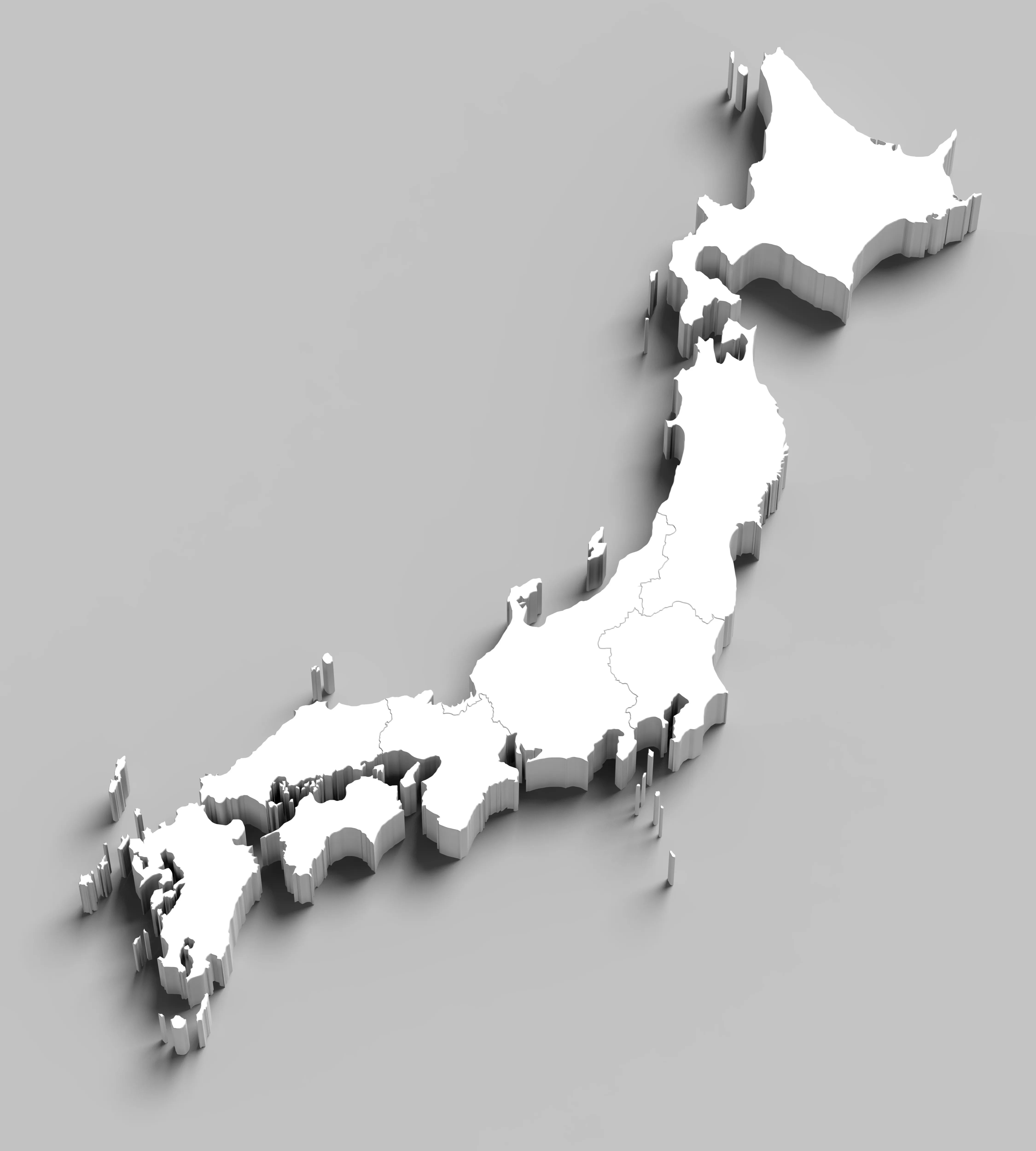
Kyushu, the third largest island in Japan, is home to the semiconductor production bases of integrated device manufacturers (IDMs) with world-class cutting-edge technology. SONY, Toshiba, Hitachi, Mitsubishi, Fujitsu and Nissan are among the sector’s shining stars, though a host of other IDMs tied to the supply chains of other major enterprises have also set root in Kyushu. Collectively, the companies earned Kyushu the name Silicon Island of Japan.Kyushu’s flourishing IDM industry sprouted from favorable tax and other government policies that reduced semiconductor production costs to levels lower than elsewhere in Japan. Once the IC producers had established bases, equipment and materials companies naturally followed, leading to the influx of many parts manufacturers. Together, they came to Kyushu, one after another, to make the island a magnet for manufacturing. And so it was to Kyushu that a SEMI China delegation travelled for a meeting at TEL’s factory in Kumamoto to learn more about the secrets to the rapid growth of the island’s semiconductor industry and promote cooperation between Chinese and Japanese enterprises. Underscoring the rise of the Silicon Island of Japan, China will soon become TEL’s largest market, said Masami Akimoto, Chairman of Tokyo Electron Kyushu Limited, speaking at the event. Masami Akimoto hopes for support from SEMI China.The island of 12 million people contributes to the growth of the global semiconductor industry, expected to reach USD 500 billion in size in 2019 as China’s semiconductor sector, fueled in part by government-backed investment funds, continues its rapid expansion. Despite the gains, China still lags other regions in advanced manufacturing, said Lung Chu, president of SEMI China, which is doing its part to draw more advanced manufacturing to the region through its SIIP platform. The initiative encourages pan-regional cooperation with China’s semiconductor industry to promote free trade, open markets, technology innovation and IP protection – all to help China better integrate with the global semiconductor industry. SEMI China President Lung Chu(L) issues visit memorial to Masami Akimoto(R), Chairman of Tokyo Electron Kyushu Limited. Chicken shall be led by the HenUnlike other regions with comprehensive semiconductor industries, Kyushu’s is primarily focused on production and assembly, with more than 200 manufacturers of semiconductor equipment and parts.SEMI China Delegation at Tokyo Electron Kyushu LimitedTEL built its first factory in Kumamoto, a city covered by volcanic ash in the center of Kyushu, 34 years ago. Today, TEL every month produces 80 to 90 sets of equipment, each consisting of, on average, over 400 thousand parts that must be certified and authorized by TEL before delivery to its module manufacturers and assembly into complete machines. Having blossomed over the past few decades, the island’s supply chain now supplies TEL with all its equipment parts. SEMI China Delegation at Fajita WorksTEL supplier Fajita Works, a high-precision plate metal manufacturer founded in 1945, is emblematic of other companies in the Kyushu supply chain. It keeps a low public profile as it serves several longtime customers and earns ardent loyalty from its workers, an ethos reflected in the change next January of its slog from “Only One” to “Great company, Great life.”Quality is the life of the enterpriseLong before the rise of its legendary automobile and consumer electronics companies, Japan was known for inferior, counterfeited products, labeled “Made In USA” and shipped to the United States by more than 100 factories. The net effect was to shrink and commoditize American markets. The tide in Japan’s product quality and stained reputation began to turn in the 1980s, when Japan’s semiconductor industry began to produce memory with an error rate 27 times lower than its U.S. competitors, giving Japan an upper hand in quality that it would never relinquish. SEMI China Delegation at HORIBAKyushu-based flowmeter supplier HORIBA, among the many Japanese companies famous for their product quality, ships 38 percent of its products into the automotive market and 27 percent into the semiconductor sector. Cleanliness is as vital a part of the company’s culture as quality. Each depends on the other, with fine detail held to the highest importance. On its visit to HORIBA, the SEMI China delegation, passing by an office area before entering the factory, sighed at the sight of the spotless, neatly kept furniture and workspace: They had never seen an office so sparkling clean. HORIBA’s success is rooted in immaculate offices, factories and the company’s motto “Enjoy innovation and pay close attention to product quality.”After Kumamoto sustained heavy damage during a 2016 earthquake, HORIBA workers returned rocks scattered by temblor to their original position, knowing that order is critical to lean, efficient manufacturing and that, indeed, “the devil is in the details.” SEMI China Delegation in Kumamoto City Full confidence in the exploration of Chinese marketConsumer electronics stalwarts Sony and Panasonic feature semiconductor factories in Kagoshima, the southernmost city in Kyushu and Japan, though rumor had it two years ago that Panasonic planned to pull out. The Panasonic plant, which provides batteries for Tesla, remains. The Sony facility produces image sensors for the iPhone.Semiconductor equipment maker ULVAC, SEMI China’s most important strategic partner, is also based in Kagoshima. During the delegation’s visit to the company, Lung Chu noted that while China is the world’s largest semiconductor market, the region meets just 13 percent of domestic chip demand. Stressing that ULVAC can play a crucial role in helping China become a bigger player, he expressed admiration for ULVAC’s professionalism along with hope that it will maintain its rapid growth and leverage SEMI resources to catalyze rapid development of Internet of Things (IoT), artificial intelligence (AI), and 5G technologies in China and rise into the top 10 of global equipment manufacturers. SEMI China President Lung Chu (L) issues visit memorial to ULVAC Kyushu President and CEO Kenji Yamaguchi ULVAC Kyushu president and CEO Kenji Yamaguchi made clear the company’s interest in Lung Chu’s insights into Chinese semiconductor industry while underscoring its core competency of producing semiconductors for flat panel displays. The Kyushu Factory of ULVAC is full of vitality and market competitiveness. SEMI China Delegation at ULVAC EBARA, a precision machinery company located in Kumamoto, has manufactured chemical-mechanical planarization (CMP) equipment for over 20 years and delivered nearly 2,400 mechanical polishing machines worldwide. While the company expects to ship 50 sets per year to China starting next year, it has the capacity to deliver 20 sets per month, enough to meet demand of Chinese semiconductor makers. SEMI China Delegation at EBARAThe most telling takeaway from the SEMI China delegation’s visit to the Kyushu: Japan ranks number one worldwide in research and development (R D) investment as a proportion of GDP and is also at the top in the percentage of R D funds controlled by private enterprises. The outsize investment strategy has enabled Japan to maintain its hold as one of the world’s top technology innovators.Like Sakurajima, the famed Kyushu volcano, the SEMI China delegation will continue to harness its forces to build relationships with the island’s semiconductor supply chain as it works to develop win-win pan-regional relationships and foster the growth of China’s semiconductor industry. Best view of Sakurai volcano Gang Yao is a marketing director at SEMI China.
Read More
What’s next for smarter, more connected electronics manufacturing - Part 3 The fast-maturing infrastructure now enabling analysis of exponentially larger data volumes brings the microelectronics industry to an inflection point, where the winning companies will be the first to master the use of this data to solve the industry’s emerging challenges. SEMI expands its coverage of these vital issues with a Smart Manufacturing Pavilion and three days of talks SEMICON West, July 10-12 in San Francisco. While deep learning is starting to be applied to image recognition for wafer inspection, it is also being considered for sequential pattern recognition in order to evaluate equipment parameter traces. The next emerging applications will start to use those learned patterns to predict outcomes, and then use those predictions to automate process control. One early application of deep learning is IC process development. “People don’t think of research and development as the first place to automate, but it’s where applying our digitization and simulation has first had impact,” says David Fried, Coventor vice president of Computational Products. He noted that insertion is easier in the lab than in the fab. Technology at 10nm and beyond is now so complex that companies at the leading edge must use process modeling to understand the effect of process variation on their designs. Learning cycles can now be accelerated during development by simulating 10,000 digital wafers instead of running 25 actual wafers during screening, Fried says. Applying structured analysis and machine learning to the data simplifies optimization across the 500 or more interrelated process steps. Coventor has recently introduced a statistical analysis package that aids the design and analysis of process variation experiments by using large volumes of data from its models. Fried says these models are next being used to accelerate the yield ramp in manufacturing. Digital simulation also could speed development of high-mix, lower value products While digital twins are best known for their use in complex, high value products like jet engines, the simulation technology could also enable the electronic manufacturing services (EMS) sector to reduce the time, cost and risk of developing its high mix of products. “The EMS sector’s use of digital twins will be vital for it to smooth the move of CAD/CAM digital design data for so many different products into manufacturing, and to accelerate validation testing of designs and products by doing more of it in the virtual world,” says Dan Gamota, vice president of Engineering and Technical Services at Jabil. Gamota also highlights the push for traceability from the automotive and healthcare markets, where the digital models could be used to quickly assure that the design was built exactly as specified. “In the past year, traceability has evolved from just ‘nice to have’ to ‘how to achieve,’” he adds. “Companies are expecting it, but aren’t willing to accept the cost and risk of doing it alone. We need the community to discuss realistic implementations, identify the most critical elements and bring together the ecosystem partners to build baseline reference architectures for key digital building blocks. The community also needs to assure the reliable flow of data among the electronic manufacturing segments from semiconductor to OSAT to EMS.” Predictive maintenance and virtual metrology applications could mature in next few years While predictive maintenance initially seemed a likely early application of machine learning in factories, it remains a challenge for the electronics sector. “The difficulty is that it’s not clear where to get the most bang for the buck,” says Tom Ho, president of BISTel America, noting that it may make the most sense to track the failure performance of a single expensive part, like an electrostatic chuck, since predicting the failure performance of a whole complex system like an etcher is much harder. “Collecting enough data from all failure types, including especially the rare events, is difficult unless you have a long history of a lot of tools,” adds Doug Suerich, PEER Group product evangelist. “The gain from collecting performance information from many tools across the industry could be big, but many companies still need to overcome concerns around exposing their IP.” Another big opportunity for prediction is virtual metrology – predicting the wafer outcome from the process or sensor data with enough accuracy to replace the physical metrology. “Virtual metrology is improving, and since metrology can be slow and expensive, any reduction could mean a huge potential savings,” says Suerich. “But it is still seen as too scary for many companies. Two to three years from now, companies will expand the practice from lower risk areas into processes that require more confidence in the results.” Moving beyond prediction to automated control needs digital models Once the results are predicted, the model can be used to control or automatically optimize a process and enable the system to learn by itself, usually by reinforcement learning on a digital model. The model can then independently make adjustments to optimize the manufacturing process. “Automated process development is getting close now. Instead of smart guys turning the knobs, deep learning is automating the smart tuning,” says Suerich, suggesting the industry could see widespread adoption in as little as two to three years. This type of machine learning needs a good digital model, and masses of data for learning. One approach uses human experts to build a physics-based model of the clearly understood parts of the process, then turns to deep machine learning to optimize the lesser-understood variables. The alternative, the data-first approach, runs a computer algorithm to suggest the solution purely from data, without human input, and then relies on the human to evaluate the usefulness of the results. Modeling digital twins of wafers could enable automated process control, chamber matching, and fleet matching, says Fried. If every wafer had its own virtual twin with all the upstream metrology and structural information needed to make equipment control decisions, it could feed forward that information to enable the seamless transition from one step in the process to another based on understanding their complex interrelationships. This could potentially improve uniformity across wafers and equipment, and reduce the need for metrology, he argues. Moving metrology sensors into the chamber will also require model-based algorithms to enable dynamic process control in close to real time, says Fried. These algorithms will be needed to acquire, parse, and process the data at high speed, and then to choose how to adjust the controls. “There will be a model behind collecting and interpreting the metrology data,” he notes. “That’s a really rich vein for improvements in process control.” “The end goal is to collect equipment data in real time, analyze it with AI, and send back controls to optimize manufacturing processes,” Jabil’s Gamota says. “This requires a robust architecture for communication between equipment and consistent formats for data collection and analysis. But the cost and complexity of this heavy lifting is too great for any one company to do alone. We need a consensus-based architecture for ingesting, analyzing and acting on the data.” SEMI tests data transfer protocols, benchmarks best practices SEMI is launching a smart data project to identify the various data transfer protocols needed for inter-company communications. The project will feature a proof-of-concept model in a development fab to produce verifiable results so SEMI can better understand how different approaches meet member needs. SEMI’s smart manufacturing technology communities and the Fab Owners Alliance are also benchmarking current smart manufacturing practices in the microelectronics industry to help SEMI members better understand the path forward and potential return on investment. Speakers over all three days at SEMICON West addressing these issues include Active Layer Parametrics, Applied Materials, Applied Research Photonics, ASML, Bosch Rexroth, Cimetrix, Coventor, ECI Technologies, Edwards Vacuum, Final Phase Systems, GE Digital, Infineon, Jabil, Lam Research, Osaro, Otosense, PEER Group, Qualcomm, Rockwell Automation, Rudolph Technologies, Schneider Electric, Seagate, Siemens, Stanford University, TEL, TIBCO Software. See semiconwest.org. What’s next for smarter, more connected electronics manufacturing - Part 1 What’s next for smarter, more connected electronics manufacturing - Part 2 Paula Doe, SEMI
Read More
What’s next for smarter, more connected electronics manufacturing - Part 2The fast-maturing infrastructure now enabling applications for big data and artificial intelligence means disruptive change not just at individual companies but also in data connections among companies across the microelectronics manufacturing value chain. SEMI checked in with some leading players on the changes they see coming in the next several years for this article series. The trade group is expanding its programming on smart manufacturing to address these industry-wide developments at SEMICON West, July 10-12 in San Francisco.“The ramp of EUV, and the smaller geometries and smaller process margins, will drive an exponential increase in the amount of metrology data to manage,” says Neal Callan, ASML vice president, Silicon Valley. Callan notes that moving to multibeam e-beam inspection will increase data volume from megabytes per second to gigabytes per second and from thousands of data points to millions of data points. “The process is so tight and the margin so small that stochastic variation, or noise, becomes more dominant – at least it’s noise until we can learn to understand and control it. And understanding and controlling this variation will be key to delivering 5nm patterning,” he says.Single-beam e-beam inspection is already driving large increases in data as engineers extend the slow technology to broad, high-speed defect metrology applications by more intelligently instructing the system where to look for problems. Callan says ASML is now using the scanner data on wafer focus, alignment and leveling. The company is also using the computational lithography model from the design to identify the smallest process windows in the pattern that are most likely to see problems. The model then quantifies the number and significance of those instances.“The collection of all this diverse data means that tools will need to be plug-and-play so all tool data is instantly available to all systems and software,” says Doug Suerich, PEER Group product evangelist. “We need tools that can be discovered automatically by the network so it can start slurping up data immediately. The adoption of the Interface A (EDA) standard is accelerating and fabs are starting to ask for it. The proliferation of sensors also needs to self-discover. If you are going to add thousands of new sensors into a facility, you can’t afford a time-consuming integration process.”“We are now seeing that engineers are greedy for more data – if they can get the data, it’s becoming a need-to-have,” adds Tom Ho, BISTel America president. “Getting more data from more sensors, from the sensors on the tool that are not being fully utilized, and from untapped data sources like vibration is another big coming opportunity.” Process complexity drives demand for feed-forward between silos with computational models ASML co-optimizes its scanner process with etch and reticle process steps. Source: ASML In addition to the drive for trace-back of data, the increasing complexity of interrelated processes is also driving demand for feed-forward of data. “Feed-forward is becoming more important,” notes Ho. He points to the example of 3D NAND features, now getting so deep that identifying the layer being measured is a challenge unless the signal at the step before can be recognized. “We need partnerships with our peers to understand how to take advantage of the sensors they use, integrate them with our data, and then feed-forward corrections to the other systems,” concurs Callan. “To drive the best CD uniformity and overlay, we need to co-optimize litho and etch,” agrees Henk Niesing, ASML director of product management. He notes that the company is working with etcher makers to measure the overlay and CD, decompose the finger prints, and then use models to steer automated control that best adjusts both the scanner and the etcher. ASML is also working with Zeiss on co-optimization between the scanner and the reticle to make even higher-order corrections by locally modifying the reticle.These higher-order corrections, applied on each exposed field, drive the need for even more data, and at higher speed but without higher cost, notes Jan Mulkens, ASML senior fellow. These corrections increase demand for computational metrology, which combines various metrology sources with physics and deep learning models trained on real data to predict and control process results in real time. “We’re working on computational metrology to ideally use all the knobs we have in the fab,” he says. So far this effort has largely involved linking data between two companies. More consistent data formats would enable data exchange to be extended to more companies. “The software versions also need to be managed for upgrades so they still match after one party updates the system on its tool,” notes Niesing. Speakers on these issues of smart manufacturing and data handling at SEMICON West include Active Layer Parametrics, Applied Materials, Applied Research Photonics, ASML, Cimetrix, Coventor, ECI Technologies, Edwards Vacuum, Final Phase Systems, GE Digital, Infineon, Jabil, Lam Research, Osaro, Otosense, PEER Group, Rockwell Automation, Rudolph Technologies, Schneider Electric, Seagate, Seimens, Stanford University, TEL, TIBCO Software. See semiconwest.org.What’s next for smarter, more connected electronics manufacturing - Part 1What’s next for smarter, more connected electronics manufacturing - Part 3Paul Doe, SEMI
Read More
What’s next for smarter, more connected electronics manufacturing - Part 1The fast-maturing infrastructure now enabling applications for big data and artificial intelligence means disruptive change not just at individual companies but also in data connections among companies across the microelectronics manufacturing value chain. SEMI expands its smart manufacturing program with a Smart Manufacturing Pavilion with displays and three full days of talks to address these industry-wide developments at SEMICON West, July 10-12 in San Francisco.Autonomous autos’ demand for zero-defect systems and 100 percent traceability back to the manufacturing data for each die is driving a push to traceability across the chip sector. “Far more chips are being used by the automotive sector, and its very different requirements are driving demand for traceability,” says Tom Ho, president of BISTel America. “Our chipmaker customers are looking for traceability solutions and the trend is the same in backend packaging and assembly – automotive applications are driving the sector to traceability.”Traceability is also driven by the growth of systems in a package as fabless chipmakers look to connect back to the packaging companies’ fault analysis labs and die interconnect history to diagnose and fix the cases where known-good die are failing in the system, adds Mike Plisinski, CEO of Rudolph Technologies. Plisinski adds that makers of consumer products like phones that can also see harsh conditions are demanding higher quality and traceability as well. The electronic manufacturing services (EMS) sector also must establish an architecture for traceability to collect critical manufacturing-related data and to interface with OSATs and semiconductor fabs. The reason is that EMS companies are adding traditional OSAT processes such as assembly of products with bare die and complex optics modules requiring clean rooms. “A unified sand-to-smart-phone smart manufacturing roadmap should be established,” says Dan Gamota, vice president of Engineering and Technology Services at Jabil. “We need to identify protocols for manufacturing data communications that can be adopted across the supply chain.”To enable smart manufacturing, vendors need to collaborate on getting their production equipment to interoperate and support factory analytics and data management systems. Source: SEMI One big challenge, of course, is how to format this diverse data so it can be linked and used by various supply chain stakeholders. “Smart data needs to be contextual and it needs data standards across the supply chain so it’s easy to link from the front end to the back end, follow common lot IDs front and back end, and have a way to map streaming data from sensors to a discrete lot ID,” notes Ho. New approaches to metrology, analysis and test that increasingly exploit machine learning on simulations will also be needed to help predict which die and connections that test well now may fail in the future as conditions change.Another issue is how to securely share the needed data across companies without jeopardizing IP. “On the equipment side we collect data across customers on how the tool is running to improve the equipment,” notes Neal Callan, ASML VP Silicon Valley. “Next we need to integrate performance and reliability data that today is not as well shared.”The other big hurdle is how to pay for data sharing. “The challenge is that the final manufacturers reap the benefit of traceability, but since they expect their suppliers to deliver good die, they don’t want to pay more for it,” notes Plisinski. He suggests that over the next two to three years, traceability and predictive fault prevention will become the norm as the automotive sector is compelled to invest in it to assure safety. Meanwhile, fabless companies will face so much complexity in integrating different die from different suppliers in SiP that they will no longer be able to afford to simply use the cheapest supplier, potentially driving a fundamental shift in relations and division of labor among fabless chipmakers, OSATs and fabs. Standards extend across supply chainSEMI member committees are collaborating to build the infrastructure to enable these developments. Standards committees are updating standards for higher bandwidth data exchange and extending semiconductor-like vertical and two-way horizontal equipment communication standards to flow shops to enable assembly players to optimize and trace back results across players. The SMT/PCBA community is integrating its smart manufacturing work into SEMI standards, and the SEMI A1 standard was a key reference document in the development of the Japan Robotics Association’s Equipment Link Protocol.Speakers addressing these issues at SEMICON West include Active Layer Parametrics, Applied Materials, Applied Research Photonics, ASML, Bosch Rexroth, Cimetrix, Coventor, ECI Technologies, Edwards Vacuum, Final Phase Systems, GE Digital, Infineon, Jabil, Lam Research, Osaro, Otosense, PEER Group, Qualcomm, Rockwell Automation, Rudolph Technologies, Schneider Electric, Seagate, Siemens, Stanford University, TEL, TIBCO Software. See semiconwest.org.What’s next for smarter, more connected electronics manufacturing - Part 2What’s next for smarter, more connected electronics manufacturing - Part 3Paula Doe, SEMI
Read More