downloadGroupGroupnoun_press release_995423_000000 copyGroupnoun_Feed_96767_000000Group 19noun_pictures_1817522_000000Member company iconResource item iconStore item iconGroup 19Group 19noun_Photo_2085192_000000 Copynoun_presentation_2096081_000000Group 19Group Copy 7noun_webinar_692730_000000Path
Skip to main content
Default Banner Image

semiconductor manufacturing

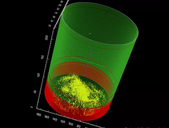
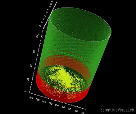
Sapphire is a precious gemstone, consisting of aluminum oxide (α-Al2O3) with occasional traces of other elements such as iron, titanium, chromium, vanadium or magnesium. While sapphire stones found in nature mostly go to jewelry applications, the lab-grown sapphire – produced in a scale of up to several hundred tons per year – is widely used by the electronic industry. Now one can hardly find a branch of technology where this crystal is not used.Sapphires are mainly applied in infrared optical components, high-durability windows, wristwatch crystals, and the very thin electronic wafers used as the insulating substrates of solid-state electronics. High thermal conductivity, low reactivity, and appropriate unit cell size make sapphire an ideal material for a wide range of such electronic substrates for manufacturing of components such as LEDs and CMOS chips.SEMI spoke with Ivan Orlov, CEO of Scientific Visual, after his presentation at SEMI Strategic Materials Conference at SEMICON Europa, 12-15 November, 2019 in Munich, Germany, to learn more about the future of sapphire.SEMI: Why is sapphire an ideal material for a wide range of electronic substrates? Orlov: Sapphire undoubted advantages are its chemical inertness and ability to withstand high temperature, radiation and mechanical loads. In addition, it exhibits low dielectric loss and very good electrical insulation that makes sapphire a good candidate for substrates for LEDs and laser diodes or wafers for epitaxial growth. However, the most important advantage is that sapphire crystal lattice does very well matching semiconductor materials deposited to its surface, in particular nitrides of group III elements. To plainly benefit from these features, the grown sapphire must have as few macro- and micro-defects as possible, as substrate defects are inherited by semiconductors layers grown on the substrate surface. Hence the importance to detect defects in the raw sapphire material. This is the area where our team at Scientific Visual contributes. SEMI: Flaws are usually identified only after costly wafering and polishing steps, because rough surface of raw crystals prevents detection of the defects. What can be done to prevent defects?Orlov: Today, major players are investing in growing larger crystals without mastering in depth the growth process. Let’s face it, the semiconductor substrate industry, which is primarily based in Asia, is using empirical research methods. The raw sapphire boules are still inspected manually, and this qualitative assessment is exploited in two folds. The first step is to further process the boule. Furnace operators then adjust the growing parameters depending on the results of the manual inspection.Due to the lack of visibility into internal crystal defects, the crystal growth and its downstream processing remain an art rather than a science. The primary reasons are the difficulty to measure, locate and quantify precisely the defects in the full crystal volume. Scientific Visual equipment enables defects in raw boules to be fully quantified and categorized. With such objective measurements and knowing the full set of growth parameters, the Process Engineering (PE) team can, with the assistance of deep learning algorithms, considerably improve the growing process. Our quality control tools give Process Engineering team the “eyes” to see complete defect distribution in raw crystals, enabling it to make minor modifications in the growth process to improve yields, reduce costs and shorten the time to market for products.SEMI: What lead to those advancements and what problems did your team set out to solve? Orlov: Breakthroughs in immersion tomography, machine vision and parallel computing drove advancements in automated quality control technology. Previously crystal inspection accuracy was limited by the acuity of the operator’s eye and subjective bias. Light distortion and the diffusion of crystals made it impossible to accurately identify internal defects.Scientific Visual equipment give operators an undistorted 3D view of all defects in a crystal boule or ingot. However, only deep learning technology can correlate a hundred thousand growth data points to identify a final defect pattern.Defect pattern in non-processed item cored from EFG sapphire plate. Well visible is a typical wavy pattern of surface layers and sandwich structure in the volume. Color code marks sapphire defect density: from deep blue (non-defective material) to deep red (highest defectiveness.) SEMI: What challenges are addressed by your approach? Orlov: Increasing the yield of semiconductor substrates like Sapphire, Gallium Nitride and Silicon Carbide is paramount to reducing the price of wafers while increasing their quality. The upstream growth and downstream wafering processes are not deterministic. So far, most of the producers can only determine the quality during the late stages of the process. This condition creates huge constraints for teams in charge of production and processing. Automated Quality Control (QC) at the early stage of the production chain relieves all the unknowns, ultimately reduce the cost of material.SEMI: And what are the main opportunities?Orlov: There are massive opportunities to increase the yield and to ease the full processing chain from growth to the wafering process. Objective Quality Control (OQC) paves the way to industry-wide standards that categorize crystal quality at each step of growth to enable full certification of the defectiveness of the material and facilitate its trade and exchange.SEMI: What’s one of your predictions for the future of new materials?Orlov: The explosion of e-mobility and electric vehicles and the development of other green technologies will drive rising demand for low-defect sapphire, silicon carbide and gallium nitride substrates thanks to the streamlining of the full processing chain. Manual quality control will soon give way to full automation as quality control in sapphire and other raw crystals production is the only missing link in a fully automated semiconductor production chain. I believe that in five years, automated raw crystal inspection will become standard in the industry. Our mission is to empower every crystal grower to achieve this important milestone.Dr. Ivan Orlov obtained a Ph.D. in Crystallography from the Federal University of Technology in Switzerland EPFL and an MSc in Solid-State Physics in Moscow, Russia. Ivan co-founded Scientific Visual in 2010 to answer the challenge of the synthetic crystals industry struggling with high defect yield. Prior to this he worked in a company specialized in diamond optics. He has more than 10 years of experience in R D with focus on optical materials, industrial crystals and non-destructive quality control technologies. Dr. Orlov was a SEMI Task Force member for sapphire standard development in China and collaborates with ISO committee in Switzerland to establish industry-wide sapphire quality standards.Serena Brischetto is senior marketing and communications manager at SEMI Europe.
Read More
On July 1st, Japan’s Ministry of Economy, Trade and Industry (METI) announced updated licensing policies and procedures on the export and transfer of controlled items and their relevant technologies to the Republic of Korea (ROK). METI’s stated purpose for the actions were “in order to ensure appropriate implementation of export control.”In particular, METI will tighten controls on certain items and their relevant technologies as follows: Remove the ROK from its “white list” of trusted partners, limiting the ROK’s preferential treatment for exports Mandate individual licenses for exports of certain chemicals including fluorinated polyimide, photoresist, and hydrogen fluoride – all used in semiconductor and electronics manufacturing – and technology transferred with exports of manufacturing equipment to the ROK. Bulk licenses for the chemicals will no longer be available. METI has indicated that its actions were not intended as punitive, but rather as necessary to ensure proper management of the export control system and the effective tracking of chemicals, materials and technologies that could be used to develop weapons of mass destruction (WMDs). Nevertheless, the trade actions are cause for concern as they could have a negative impact on our members operating in Korea and Japan and the global supply chain in general.After the METI announcement, SEMI immediately consulted its International Board of Directors and assembled a global advocacy response team comprised of SEMI member companies and SEMI regional presidents in both Japan and Korea to assess risks to SEMI members operating in both regions and to the industry’s global supply chain. Additionally, SEMI conveyed its concerns to Japan and ROK trade officials, stressing that the semiconductor industry will bear the brunt of the new measures if the trade dispute escalates.SEMI president and CEO Ajit Manocha said: “We informed both governments of potential impacts of an escalation to SEMI members, their economies and the global supply chain and are encouraging them to resolve their differences. SEMI’s focus is to ensure the global microelectronics supply chain remains strong and intact.”SEMI member companies have stated that METI and the Japan government have provided assurances that trade with the ROK will not be encumbered and that semiconductor companies will see minimal impact regarding export license approvals. To this end, SEMI will continue to engage our members in Korea and Japan, monitor the dispute as it continues to unfold, and facilitate regular meetings between industry and the involved governments to ensure that industry impacts are identified and risks are mitigated. In the event the dispute escalates, SEMI is prepared to take action in accordance with its Global Trade Principles.SEMI released its Global Trade Principles last year to provide guidance to governments around the world in developing policies that benefit both regional economies and the industry. These trade principles are based on SEMI’s four trade pillars of free and fair trade, open markets, supply chain growth, and respect for IP and national security.Member companies negatively impacted by any changes in Japan’s regulatory policies or with any questions should contact their regional SEMI office or Jay Chittooran, Public Policy Manager, SEMI Global Advocacy, at [email protected] Russo is Vice President of Global Industry Advocacy at SEMI.
Read More
Semiconductor, electronics and equipment manufacturers today face a number of logistics and supply chain challenges that could be overcome by systems providing a secure, tamper-resistant, single source of truth. Chief among these challenges is limited data sharing due to data security barriers among suppliers, shippers, manufacturers and test houses, an impediment to achieving optimal product quality and regulatory compliance. Additionally, inefficient and inadequate processes for tracking goods make it more difficult to isolate shipping problems, track faulty parts and verify product authenticity. Counterfeiting has become a serious problem that costs US-based semiconductor manufacturers $7.5 billion annually.How Blockchain Can Help Clear Data Sharing BottlenecksBlockchain functions could help alleviate many data sharing pain points in manufacturing. Blockchain’s distributed functionality, bundled security measures, and associated features such as smart contracts have the potential to help manufacturers quickly trace goods, manage records transparently, and automate supply chain processes and payments. No isolated blockchain platform would solve all of these problems on its own. But, when combined with other solutions and applied to particular use cases, blockchain has the potential to optimize operations and foster an environment of trust and collaboration among consortium members. Three core features of blockchain make it a valuable technology for manufacturing: Distributed and immutable system of record. With a distributed system of record in the blockchain network, there is no "central" data store controlled by one organization. The distributed ledger provides all participants with a view into the data, thus increasing transparency, data distribution timeliness, information sharing, and data access. Security also improves as there is no single central data store open to external attacks. Once data is inserted onto the chain, it cannot be easily changed. Security and Trust. Blockchain integrates best-of-breed cryptographic mechanisms to guarantee the digital identity of the network participants and secure the privacy of the data stored to enable role-based data access. It brings trust to a potentially trustless environment without the need for a centralized third party. Smart Contracts. Smart contracts are embedded business logic that can be added to a blockchain. They enable the automation of many processes and the secure handling of contracts. Blockchain Use Cases in ManufacturingIn each stage of manufacturing, blockchain could be applied in a variety of use cases to expedite processes and alleviate security issues. A few examples that merely scratch the surface of what may be possible follow.In pre-production, manufacturers may implement blockchain solutions for Collaborative Planning, Forecasting and Replenishment (CPFR). These systems monitor inventory levels, enabling suppliers to replenish supplies before they run low. The expensive, proprietary B2B networks used today could be replaced with blockchain as the common sharing protocol, using non-proprietary or public networks.Suppliers may also combine blockchain with IoT sensors on shipping containers to provide a tamper-resistant record of shipping conditions. This could be used to ensure that temperature and humidity tolerances for chemicals and equipment are not exceeded during transit from the supplier. The identity and materials in components and subcomponents of manufacturing equipment could be collected on a blockchain to verify compliance with environmental and health regulations. During production, a manufacturing process machine can be registered on a blockchain with a unique identity; its performance and maintenance history can be recorded. A maintenance service provider could then be automatically notified, via a smart contract, when a predictive maintenance alert is written, allowing repair of machines before they fail. In the distribution stage, customers could search the ledger for a product’s complete history, reducing counterfeiting and solidifying the origin of properly sourced goods. When faulty product is identified, the manufacturer may search the ledger to quickly locate the faulty supplier or bad test results and alert all receivers of the defective product.ConclusionWith blockchain, manufacturing can become a more collaborative process among suppliers, manufacturers and customers. Blockchain can help streamline the supply chain and inventory replenishment, improve tracking and regulatory compliance, and reduce counterfeiting. Augmenting blockchain with IoT enables use cases like predictive maintenance and monitoring of goods during transit. Blockchain is not yet mature and its business value still needs to be proven. However, it is poised to help manufacturers decrease costs and fraud, and provide customers with faster, more secure delivery, increased visibility, and consistency.More Resources on Blockchain and ManufacturingTibco is an active member of SEMI’s Smart Manufacturing Technology Community, which holds regular meetings on this and other topics. Join now to help shape the future of Smart Manufacturing. For more information on blockchain use cases in manufacturing, please see these resources. Read this Whitepaper: Blockchain and Manufacturing: A Match Made in the Factory Watch this Webinar: Blockchain and Manufacturing - A Match Made in the Factory Visit the TIBCO Blockchain Solutions page Mike Alperin is a TIBCO principal manufacturing industry consultant embedded in the Data Science team where he applies analytics, machine learning and big data technology to current industry problems. Prior to this he was the product manager for a leading commercial yield management application. He has worked at start-ups and global semiconductor manufacturing companies as a yield manager, device engineer, process engineer and failure analyst. Mike is based in Austin, Texas.
Read More
Critical subsystems for the IC equipment market continued to grow to a new record of $11 billion in 2018. While 2019 is expected to be a downturn year, the long-term outlook remains unchanged with an average growth rate of 3 percent. Last year may have been a new high for revenues, but it will be remembered as a year of two parts: record quarterly revenues in Q1, followed by rapidly falling orders in Q3 and Q4. Normally, this would not be a problem as suppliers are used to managing volatility in their businesses. However, encouraged by solid end market drivers and optimistic customers, the timing of this downturn was particularly bad as it coincided with the addition of significant new manufacturing capacity for critical subsystems that will be needed to supply the industry into the next decade. The resulting step change in costs against the backdrop of falling revenues has put strain on the financials of these suppliers. Although current visibility is poor, the order decline appears to be stabilising and the worst is nearly over. Revenues are expected to recover in the second half of 2019 followed by a promising outlook for the following three years. Critical Subsystems for IC equipment history and forecast to 2022. After a pause in 2019, the trend is expected to continue to reach new industry records. Suppliers of subsystems used in vacuum process tools, such as deposition and etch, have benefited the most from critical subsystems growth since 2012. Vacuum intensity of semiconductor processing continues to grow and in 2018 the value of vacuum process tools exceeded the value of non-vacuum process tools for the first time. This trend is expected to continue with vacuum based semiconductor process equipment accounting for over 60 percent of wafer fab equipment revenues by 2023. In summary, 2019 is expected to be down 10 percent to 20 percent as the industry digests the recent large additions to semiconductor manufacturing capacity, followed by a new cycle starting in 2020.Julian West is a technical and marketing analyst at VLSI Research Europe.
Read More
SEMI met with Jay Zhang, business development director at Corning Incorporated, to discuss recent innovations at Corning that allow fine granularity CTE engineering as well as high Young’s modulus. We also talked about the impact of this work on in-process warp control, as well as the associated production methodology that provides rapid prototyping and high-volume manufacturing. We spoke ahead of his presentation at the 3D Systems Summit, 28-30 January, 2019, in Dresden, Germany. To register for the event, please click here.SEMI: What is Corning’s mission and vision and your role within the company?Zhang: Corning is one of the world’s leading innovators in materials science with a track record of 165+ years of life-changing innovations. We excel in glass science, ceramics science, and optical physics and succeed through sustained investment in RD E. Our products include Corning® Gorilla® glass, a durable material used on more than six billion mobile devices worldwide, and industry-leading LCD glass for display applications. We have recently dedicated a unit of the company called Precision Glass Solutions to address the emerging need for glass in the semiconductor industry. Here we apply Corning’s long history of glass science expertise and deep customer relationships in consumer electronics to support cutting-edge applications like wafer-level optics for precise 3D sensing and carrier solutions for temporary bonding applications in semiconductor manufacturing. It’s our most recent work in the Carrier Solutions product line that I’m excited to present: a new carrier glass product optimized for fan-out, called Corning Advanced Packaging Carriers.SEMI: What projects are you currently working on that you think will make a difference in 2019?Zhang: My team is excited to introduce Corning Advanced Packaging Carriers this year. This is a new line of product within our portfolio of Carrier Solutions. These ultra-flat glass carriers are specially developed to reduce customers’ challenge of in-process warp by up to 40 percent, which in turn helps advanced packaging customers achieve better yield.Corning Advanced Packaging Carriers feature high-stiffness properties and are available in a wide range of coefficients of thermal expansion (CTE) in fine granularity. These attributes help customers select an ideal glass carrier that will minimize in-process warp for their package. Furthermore, we make sample quantities of these carriers available in just four to six weeks to help maximize efficiency during customers’ R D process.My team is excited about the potential of this new product, but also encouraged by our results. We have already supplied this product and have heard from one of the largest semiconductor companies in Taiwan that it has reduced in-process warp by as much as 150μm.SEMI: Your presentation at the 3D Systems Summit will focus on Agile Manufacturing of Glass Carriers for Advanced Packaging. What exactly will you be sharing?Zhang: There is a lot of interest right now in using glass as a carrier substrate in temporary bonding applications in advanced semiconductor packaging – especially in fan-out processes. We also know that in-process warp is a significant challenge to companies pursuing advanced packaging because different CTE materials are added during the process. My team has done a lot of work to understand the impact that an ideal CTE glass carrier substrate can have on minimizing in-process warp. We have studied the available levers – both theoretical and in real-life fab environments – that can help address this challenge. I will present our findings on how it is possible to select a glass carrier with the ideal CTE and Young’s modulus to reduce in-process warp by up to 40 percent, and how Corning has developed an agile manufacturing platform to support customers with these ideal carriers from their R D stage through mass production.SEMI: What do you think will be a hot topic in the next few years?Zhang: We expect high-end fanout technology to address more applications beyond just mobile APs. There is also an interesting dynamic playing out between wafer-level and panel-level fan-out technologies. Corning is active in both areas. In developing and offering high performance glass carriers, we hope to help enable our customers to expand the fan-out applications space.SEMI: What are your expectations regarding the summit in Dresden, and why do you recommend your members and other industry leaders to attend the 2019 3D Systems Summit?Zhang: Europe is where some of the most advanced packaging technologies are born. Fan-out also saw early commercialization there. I hope to meet many scientists and technologists at 3D Systems Summit and exchange technical and business ideas. We also hope to get early feedback from other attendees about the value of our new product offering. Serena Brischetto is a marketing and communications manager at SEMI Europe.
Read More
SEMI met with Erez Halahmi, vice president at 0eC SA, to discuss a new way to transfer information not only between chips but also between servers to reduce power consumption while boosting performance. The two spoke ahead of his presentation at the 3D Systems Summit, 28-30 January, 2019, in Dresden, Germany. To register for the event, please click here.SEMI: What is Zero energy connection’s (0eC) mission and vision and your role within the company?Halahmi: Prof. Naaman of the Weizmann institute of Science (Israel) and I founded OeC SA and invented the Zero energy connection (0eC) technology. OeC SA offers a completely new and innovative solution for interconnections, which dovetails with the current technological trend of “less is more.” In fact, we constantly search for a reduction in energy consumption in favor of capacity, all while simplifying manufacturing processes. We try to look at things differently. This is why our technology is so out of the box. It is a completely new way to transfer information, not only between chips but also between servers.SEMI: What projects are you currently working on that you think will make a difference in 2019?Halahmi: I am working on several diversified exciting projects including the development of a planar field emitter and a rechargeable battery with energy density higher than 1KWh/Kg. Planar field emission is a field emitter made with standard FAB processes that enable a pixelized matrix of emitters at the resolution of photolithography. The rechargeable battery is a novel battery type that delivers unprecedent energy density.SEMI: Your presentation at the 3D Systems Summit will focus on a new way to transfer data. Why is this a key topic?Halahmi: Metals have been used to transfer data since the realization of the first integrated circuit by Jack Kilby in 1958. What happened next? Photonics slowly entered the market supported by huge investments, and the global market grew over the years. However, even with such enormous growth, photonics is not easily integrated with CMOS processes and the market also faces the conversion energy issue on top of the rising costs of process change. Integrating photonics with CMOS requires converting an electrical signal to a photonic signal and back. This costs energy and adds circuitry complexity. What to do? We identified a need to create something out of the box – on one hand using the same CMOS processes without conversion, and on the other hand significantly increasing performance. More details will be released at my presentation at the 3D Systems Summit in Dresden. I am certain that you will find our invention very intriguing. SEMI: What do you think will be the main focus in the future?Halahmi: My belief regarding many aspects of our life is that history repeats itself. Look for example at the comparison Gallium Arsenide (GaAs) versus Silicon (Si). GaAs was never able to defeat the simplicity of Si. The same applies to data transfer. However, for a solution to overtake the metal interconnect, it is not enough to offer many advantages, but the same order of production simplicity should apply. Consequently, big companies will continue to focus on metal solutions for transferring data, though some smaller companies might adopt our technology due to its relative simplicity of production and great benefits.SEMI: What are your expectations for the summit in Dresden, and why do you recommend other industry leaders to attend the 2019 3D Systems Summit?Halahmi: The summit is a great opportunity to learn about new technologies and meet the people behind these innovations. It is a unique chance to meet and question the inventors themselves and learn more about your competitors. See you soon in Dresden!Serena Brischetto is a marketing and communications manager at SEMI Europe.
Read More
SCIS is a SEMI Technology Community that tackles critical component defectivity for the semiconductor manufacturing industry. The organization develops test methods for measuring defects in these critical components. Originally, this SEMI community was looking at challenges surrounding sub-10nm process nodes, but our constituents – Integrated Device Manufacturers (IDMs), capital equipment OEMs, and (sub)component suppliers – felt that the immediate need was for standards that would apply to process nodes that are already being used for volume semiconductor device manufacturing.IDMs need ways to tell their supply chain how defects attributable to these critical components factor into the overall process-node defect budgets and wafer-contamination limits. Chipmakers and IDMs needed to start with a baseline: How problematic are existing critical components in the overall fab systems and how do these contaminants contribute to defects and how do they affect overall process yields?These questions must be answered for every component in the fab’s process line including the drums that hold the fab chemistries, fluid delivery systems, and components used in the wafer-processing chamber. All of these critical fab-line components come into contact with each manufactured wafer, in one way or another, and each is a suspect with respect to contamination, defects, and yield problems. SCIS develops test methods for these fab-line critical components testing that are used to identify the defects caused by these components and for establishing baselines.SCIS has seven working groups dealing with various critical components. Each is developing various test methods for many critical fab-line components. There are many facets with respect to testing each of these critical components.Take something as simple as a seal, such as an FFKM (perfluoroelastomer, made from polymers) seal. These seals are ubiquitous in fab lines. In harsher environments, such as inside of a processing chamber, these seals are exposed to high temperatures and harsh chemistries. Different FFKM seals will have different characteristics such as thermal resistivity and chemical resistance, depending on customer specifications, and can also vary from one manufacturer to another. In addition, these characteristics can change depending on environmental conditions – or just the passage of time.SCIS looks at defect traits from the perspective of each component in the fab line and decides which of the components’ parameters contribute most to process defects. Initially, the SCIS Seals Valves Group collected a list of seal-related issues or parameters. The working group then cross-checked these parameters against different manufacturing processes used in the fab including ALD (atomic layer deposition) and CVD (chemical vapor deposition). Some processes are harder on seals than others. Then the working group prioritized these various parameters according to their contribution to the overall process defect budget. IDMs provided important input during these steps because they work with these seals on a daily basis. At this point, the SCIS working group had a prioritized list of parameters, vetted by various stakeholders in the semiconductor manufacturing industry. The group then set to develop standardized measurement methods for these critical parameters.Based on this work, the SCIS Seals Valves Group has already published two documents. The first is a standard that specifies methods for testing seal-induced impurities such as ashing (analysis of metals content of the ash) and TOC (total organic content).The second document published by the Seals Valves Group is a guide that documents BKMs (best known methods) for handling seals – from the moment they’re cured in an oven to packaging, shipping, handling in a fab, and installation – to reduce contamination problems during use. For example, some seals are sensitive to light. Some polymer seals degrade when they come into contact with IPA (isopropyl alcohol), which is often used for prepping. A degraded seal can emit contamination particles during processing, which will cause yields to fall. (This latter bit of information came directly from a major IDM, which demonstrates the invaluable role that users of these components can play in the development of testing standards.)The Seals Valves Group’s current work focuses on developing a standard for measuring seal leak rates. This standard will define test methods for evaluating a seal’s ability to maintain pressure under vacuum. Although there are well-established standard for testing seal CSR (compressive stress relaxation) in the aerospace industry, there’s no such standard for the semiconductor industry. So originally, the Seals Valves Group tried to tackle that challenge by developing a similar standard for SEMI’s constituents. However, a more practical and immediate parametric challenge turned out to be seal leakage rates.Installed seals are exposed to high temperatures and harsh chemistries in the semiconductor fabrication process. The Seals Valves Group decided to develop a test method that would determine how well seals perform over time with respect to leakage rates as the seals are exposed to cyclic harsh conditions. The goal is to simulate the working conditions for these seals, as closely as possible and in a repeatable manner.There are, of course, some challenges associated with this work. For example, IDMs and equipment OEMs don’t want to reveal their exact process conditions as they are proprietary. So the Seals Valves Group took a step back and focused on developing a test method based solely on exposure to elevated temperatures.Development of this thermal test requires the design of a standardized test jig to help ensure consistent, repeatable tests, shown in Figure 1. Figure 1: Elastomer seal test jig developed by the SCIS Seals Valves Group.The seal under test, shown in red in Figure 1, sits at the center of the jig. A second seal, shown in green, is used to seal the actual test environment. Two thermocouples in the jig’s top and bottom monitor of the temperature inside of the jig. There are gas and purge lines for controlling the ambient pressures on either side of the seal under test.Figure 2 illustrates how the jig is connected to the gas sources. Figure 2: The Seals Test Jig is connected to helium and nitrogen gas sources and to a calibrated leak (vacuum) line. The seals leak test is based on a helium leak test. Helium is one of the smallest atoms so it will leak through just about any small gap and, with time, permeate through the material as well. In addition, helium is inert, and testing for helium using a mass spectrometer is a well-established technique for leak testing. Helium leak testing can be one thousand to one million times more sensitive than using mechanical, pressure-decay test techniques. The jig’s nitrogen lines serve to purge the test chambers of helium between leak tests.Developing just a test jig is not sufficient. The Seals Valves Group also developed a test sequence for using the jig. There were no existing standard, so the group needed to use its knowledge of the seals’ composition and operating conditions to develop certain test parameters. For example, the group elected to use 200°C as the maximum temperature for the high-temperature portion of the test because FFKM seals start to degrade at 250°C.At this point, the Seals Valves Group has gone through several iterations of a proposed test sequence. There was some initial reluctance to provide detailed inputs, but after a few iterations of the proposed method (and an understanding that this would become an industry standard to hold suppliers accountable), inputs have become more forthcoming.This is an excellent example that demonstrates why it’s so important for SCIS working groups to get chipmakers, IDMs, component vendors, and even feedstock materials vendors to participate in these standardization efforts. Standards are far more useful if they’re based on real-world conditions.Currently, the SCIS Seals Valves Group is working towards finalizing the seals-leak test sequence. The jig has been designed in AutoCAD and a prototype will soon be manufactured. Although the test and jig have been developed with significant industry participation, the validity of the test has yet to be determined. The validity will be verified though Alpha testing before the jig design and test method are incorporated into a standard.However, SEMI is not a test house. It’s a facilitator. The testing will therefore be performed by a neutral third party capable of carrying out the test under fab-like conditions. SEMI’s role is to work with different testing entities such as SUNY Polytechnic Institute in Utica, New York or IMEC in Belgium.SEMI will solicit bids for this work through its SCIS Executive Advisory Committee, which consists of C-level executives from device makers, semiconductor capital equipment OEMs, and major critical component suppliers. This project has leveraged many of the relationships that SEMI has developed over the years and has broken new ground in standards making for SCIS and for SEMI.For those looking to learn more about SCIS or engage in ongoing efforts, please contact Paul Trio, senior manager of Strategic Initiatives at SEMI, at [email protected].
Read More