downloadGroupGroupnoun_press release_995423_000000 copyGroupnoun_Feed_96767_000000Group 19noun_pictures_1817522_000000Member company iconResource item iconStore item iconGroup 19Group 19noun_Photo_2085192_000000 Copynoun_presentation_2096081_000000Group 19Group Copy 7noun_webinar_692730_000000Path
Skip to main content
Default Banner Image

semiconductor manufacturing

As the global economy is constantly transformed, the need for new skills has never been higher. The microelectronics industry is thoroughly affected by this urgent need. To develop a workforce fit for the future, it is crucial to invest not only in reskilling and upskilling, but also in skills anticipation and inclusivity. To tackle this need, the European microelectronics ecosystem has adopted many bottom-up initiatives and good practices supporting lifelong learning. Many companies collaborate with universities and training institutes to offer work-based training, and numerous events take place to support women participation in STEM and to attract more young talent to a microelectronics career. Despite these great efforts, further pooling of investments is necessary if Europe is to develop efficient lifelong learning programs. Creating strong skills partnerships is vital for sustainable upskilling and reskilling initiatives. According to the World Economic Forum (2021), greater private-public collaboration on large-scale upskilling and reskilling initiatives could boost global GDP by $6.5 trillion and lead to the creation of 5.3 million net new jobs by 2030. What is the Skills Partnership? Against this backdrop, SEMI Europe is launching the Skills Partnership for Microelectronics. The partnership brings together industrial and education partners from the microelectronics ecosystem to implement the Pact for Skills, an EU initiative which aims to boost upskilling and reskilling investments in key ecosystems for Europe’s competitiveness. Following the high-level roundtable with SEMI Europe’s Advisory Board, hosted by European Commissioners Thierry Breton and Nicolas Schmit, the microelectronics sector was selected in November 2020 as one of the key ecosystems for the first wave of implementation of the Pact, alongside automotive and aerospace/defense. Read more details about the October 2020 roundtable. 59 partners have already endorsed the Pact for Skills for Microelectronics. The Skills Partnership for Microelectronics aims to: Exchange good practices of upskilling and reskilling initiatives of the microelectronics industry Develop sustainable collaboration mechanisms that will monitor microelectronics skill needs, learning from the examples of the METIS blueprint project Promote the microelectronics sector as a career choice Boost the presence of women and other under-represented groups in the sector. The partners will have the opportunity to liaise not only with European, but also with national and regional authorities and clusters, so that a pan-European holistic approach to microelectronics skills development is achieved, and a significant flux of public and private investments on skills is mobilized. To launch this ambitious partnership, SEMI Europe held an initial workshop on March 17. Participants included representatives from the European Commission’s DG Connect, DG Employment and DG Grow, national and regional authorities, and over 70 industry and education partners. The workshop opened with representatives from the European Commission informing all stakeholders about the Pact for Skills initiative, as well as about EU skills-related funding opportunities. In the framework of the Pact for Skills, the Commission will support the ecosystems with a Networking Hub, a Knowledge Hub and a Guidance Resources Hub. These platforms will be available later in 2021 and will act as a one-stop-shop to support the partners and provide information on EU policies and funding opportunities. Other presentations went on to set the scene, presenting the main priorities of the partnership. Françoise Chombar, CEO of Melexis, highlighted the skills challenge experienced by the microelectronics industry. She emphasized the importance of lifelong learning and the danger of the gender disbalance in the sector and underlined the huge innovation potential and profitability that could be unleashed for Europe if the gender gap is successfully addressed. Moreover, the preliminary results of the METIS Microelectronics Skills Strategy were presented, to offer the basis for the partnership’s approach to skills anticipation. The partnership will establish working groups that will investigate the industry needs, leading to a better connection with the offer of education and training programs. Last but not least, the partnership aims to promote national and regional funding of upskilling and reskilling initiatives. In this regard, representatives from national and regional authorities and clusters participated in the meeting. The government of the Basque region had an active role, presenting the region’s priorities, incentives and main actions on promotion of lifelong learning initiatives. The next steps The meeting concluded with an overview of the next steps for the newly launched partnership. In the next workshop, the partners will align on the specific KPIs, as well as on the focus areas where they would like to engage (skills anticipation in semiconductor manufacturing, skills anticipation in semiconductor design, gender balance, etc.). In that framework, the executive board will be established, as well as the working groups that will lead the work of the partnership and set targeted objectives. If you want to take active part in the creation of this large-scale initiative, please fill in your details here. To learn more about the initiative, click here or contact [email protected]. Stefania Gavra is public affairs manager at SEMI Europe.
Read More
As the Biden administration begins to advance its policy goals through U.S. government agencies, SEMI is eager to work with these new officials and appointees to advance innovation and strengthen U.S. leadership in the microelectronics industry. SEMI President and CEO Ajit Manocha today sent a letter to Commerce Secretary-Designate Gina Raimondo advocating for strengthening American manufacturing, investing in research and development and pursuing multilateral rather than unilateral U.S. export controls. SEMI also “requests Commerce perform a comprehensive review of recent policies and formally seek industry input via publication of a Notice of Inquiry (NOI), giving industry its first formal opportunity to provide its views on these significant regulations.” The letter discusses the importance of how export controls are implemented, advocating that “multilateral controls – where items of concern are controlled by all major producing nations – create a level playing field, maximize effectiveness, and minimize harm to U.S. national security and economic competitiveness. Unilateral U.S. controls over items for which there are comparable non-U.S.-origin items are generally ineffective in supporting national security goals and are likely to erode any technological advantages enjoyed by U.S.-origin items.” Foreign availability of semiconductor manufacturing equipment, materials and design software is an important consideration for U.S. export control policy related to those items. In an appendix to the letter, SEMI provided charts detailing the foreign availability of major types of semiconductor manufacturing equipment and materials. For nearly all items, there are competitive alternatives to U.S.-origin items available from non-U.S. sources. With many semiconductor technologies concentrated in a handful of key exporting nations, the letter encourages a unified approach via a plurilateral export control regime instead of unilateral U.S. controls for these technologies. SEMI provided a framework of issues that need to be considered and properly addressed in negotiating a plurilateral agreement related to semiconductor industry export controls. The previous administration created several unilateral controls that were implemented with little or no opportunity for public or industry comment and which created several unintended consequences. In addition to the request to publish an NOI, the letter asks Commerce to correct unintended controls related to the August 2020 expansion of EAR General Prohibition Three and reduce the backlog of license and classification requests. SEMI is pleased to work with the U.S. Department of Commerce and other policymakers by providing industry data, trends and perspectives to ensure export controls effectively serve national security interests without undue harm to technological development and leadership in this dynamic, globally competitive industry. Kimberly Ekmark is director of Public Policy and Advocacy at SEMI.
Read More
D-SIMLAB Technologies, a Singapore-based provider of simulation-based business analytics and optimisation software solutions, recently joined SEMI. I spoke with Peter Lendermann, the company’s co-founder and Chief Business Development Officer, about the company’s role in the smart manufacturing movement, how customers are benefiting from D-SIMLAB solutions, and what the future holds for smart manufacturing. Ng: What is D-SIMLAB’s mission?Lendermann: Our mission is to develop, market, and deliver high-performance simulation-based decision support solutions that enable corporations to enhance their performance in a sustainable manner leading to significant cost savings. In particular, we focus on semiconductor manufacturing material flow planning and optimisation but also do business in aviation where we help customers optimise their spare parts support operations. What these two domains have in common are three important attributes: They are capital intensive, their underlying operations are complex, and operations are also heavily affected by random, i.e. unpredictable events, which makes both planning and execution of manufacturing operations very challenging. D-SIMLAB is a spin-off from the Singapore Institute of Manufacturing Technology (SIMTech) under the Agency for Science Technology and Research (A*STAR). Our head office is in Silicon Island Singapore. We also have representations in Germany and the U.S. Most of our staff are industrial and computer engineers with up to 20 years of operations experience in their respective industry domain, as well as vast data analytics and software development capability.Ng: What solutions does D-SIMLAB offer to optimise semiconductor manufacturing?Lendermann: In the three-pillar smart manufacturing framework of Connect, Sense and Predict advocated by SEMI, our focus is on Predict though we emphasise the equal importance of the subsequent Act: Our solutions can Predict, for example, WIP waves or usage-based preventive maintenance due dates. But much more value-add can be realised once some decisions with regard to how to Act can be derived from such a prediction. The ability to pro-actively adjust action plans in a timely manner is essential to overcoming challenges arising from changing customer due dates, mix profile changes, untimely production line issues, and production capacity to be shared with R D lots effectively, so that ultimately our customers can enhance capacity, reduce cycle times and improve the due-date performance of their factories.To that end, our D-SIMCON solution suite spans the full spectrum of decision-support tools required to forecast, manage and optimise material flow – from operational scheduling and dispatching, WIP forecasting and dynamic and static capacity planning all the way to specific applications for fab load mix optimisation or for the enhancement of the product/layer dedication and resist allocation in the lithography area. Our solutions are implemented in numerous 6-, 8- and 12-inch wafer fabs operated by both IDMs and foundries worldwide with capacity ranging from 40,000 to 200,000 wafers per month.Ng: What are the key enablers of D-SIMLAB’s success?Lendermann: Our success lies in deploying production-ready solutions for our customers, allowing them to extract immediate value. Our solutions enable the portrayal of many domain-specific characteristics such as queue time constraints or specific equipment behaviour, which is absolutely essential to generating operationally feasible plans or schedules in order to be able to Act in the best possible manner according to what has been Predicted. Moreover, we have modules for automatic generation, calibration and maintenance of the underlying capacity model, including resolution of data inconsistencies as well as verification and validation of the model, to allow near real-time responses to continuously changing operations. And the associated optimisation approaches focus on creating maximum possible value with as few iterations as possible and within minimum time through smart heuristics and parallel computing infrastructure – a paradigm that is as powerful as it is cost-effective.Ng: What are a few of your more notable customer successes?Lendermann: As a result of the first implementation of our novel, multi-objective based Scheduler cum Dispatcher, a tool capacity gain of 8%, a transportation capacity gain of 10%, and an operator workload reduction of 25% were concurrently realised at one of the critical equipment groups in our customer’s fab. At another set of equipment groups in the same fab, a 7% increase of lots within the critical queue time limiting area was achieved.Another use case we successfully realised is fine-tuning of Preventive Maintenance plans: Based on a seven-day lot arrival forecast at each equipment generated with our WIP Forecaster, a recommendation is made when PM would be best possible without causing too much disruption in the WIP flow. The effect of this synchronisation of the PM plan with material flow enabled a dramatic reduction of the average queue lengths at critical equipment groups and the associated cycle times without incurring any capacity loss. Reduction of average queue length as a result of synchronising preventive maintenance with material flow. Ng: What challenges has D-SIMLAB been facing in the COVID-19 world?Lendermann: Obviously, software delivery projects have become more challenging for the time being since our engineers cannot be on-site frequently. But it also turned out that more and more services can be delivered remotely, which has the nice side effect of making the services more cost-effective for customers. Overall, we are confident that our solid customer base will enable us to sail steadily through these challenging times.Ng: Where does D-SIMLAB see the technological development heading?Lendermann: In the future, enriching decision support and manufacturing execution solutions with machine learning and other AI techniques will be critical in reducing dependency on human experience. This path is essential to making manufacturing operations fully Industry 4.0-compliant. D-SIMLAB will certainly be at the forefront of this development. Bee Bee Ng is president of SEMI Southeast Asia.
Read More
Semiconductor process development is no easy task, with each generation of devices more difficult and expensive to create. Traditional cycles of build-and-test development are becoming obsolete, since they are too expensive and time-consuming for the most advanced processes.The High Cost of Process DevelopmentMost chip designers developing new products rely on existing manufacturing processes, but someone had to create those processes to make the designs possible. The goal of process development is to create new semiconductor manufacturing processes that provide high yield while achieving the required device performance. In contrast to new chip design, however, it requires an entirely different set of engineers and skills.The traditional approach to process development involves building multiple test wafers to determine the ideal process for a given device. After one set of wafers is fabricated and analyzed, insights from the previous round help to refine process steps for another round of fabrication. Due to smaller feature sizes, each new process generation is more sensitive to variation. This adds even more complexity because smaller feature sizes and parasitic effects require more measurements and testing as well as additional fabrication. The cycle is repeated many times before the entire process flow can be finalized, making it time- and cost-intensive, especially for the most advanced technology nodes.Testing Virtual Wafers Instead of Real WafersToday, there is an alternative to this slow, expensive way of doing things. Virtual fabrication lets computers simulate all of the processing that occurs when real wafers are built. These virtual models allow semiconductor process engineers to test manufacturing equipment settings with far greater variation than is possible in a physical fab. Designers can simulate the entire process flow, running the equivalent of thousands of wafers in days instead of months. Designers can quickly see graphical animations to visualize process steps, modify process recipes and device geometries, and measure how these changes affect electrical behavior.Improving Yield Using Statistics in Virtual Wafer FabricationBecause of the high volume of data generated, designers are turning to statistical analysis to provide greater confidence in their choice of process settings. Defects and random variations can be modeled in a virtual fab in a way that’s not possible in a real fab, letting developers test the sensitivity of the device structures against the unpredictable aspects of processing.There’s more than one approach to optimizing the process settings used in a new memory or logic fabrication sequence. The simplest one involves taking a single variable and exploring its effects. Critical dimensions (CDs), for example, establish those feature sizes of a device that ensure desired electrical performance. A particular dimension can be swept from low to high values – developers can then measure the effects of that range on device behaviors such as threshold voltage. This allows developers to ensure that the electrical behavior of their device design addresses the range of expected feature sizes and variability. The interactions with intersecting process steps can also be tested for further validation, since these interactions can lead to unanticipated device performance.But, in reality, this approach isn’t sufficient for studying the complex web of interactions between process steps and the resulting structures.A second approach leverages Monte Carlo analysis, randomly varying a wide range of process and device parameters and calculating the resulting device geometry and performance. This data can be used to automatically identify the process and design settings needed to achieve yield and performance goals. It’s an area where simulation shines, providing a useful way to test the interactions between many different processes.Statistical experiments using virtual fabrication illustrate step-by-step methodology to optimize process and design settingsVirtual Fabrication PlatformSEMulator3D is a virtual fabrication platform created by Coventor, a Lam Research company. It allows the definition of all process steps, the modeling of devices, the collection of metrics, electrical and device analysis, the statistical analysis of results, and the visualization of process steps through graphical animation. Today, semiconductor companies use it for both optimizing and scaling leading process nodes and for developing advanced new technologies like GAA (Gate-All-Around) transistors.The ability to do this work virtually is the future of semiconductor process development. Virtual fabrication accelerates new process time-to-market by months, opening up market opportunities worth hundreds of millions of dollars for semiconductor companies.Visualization of process steps of a Gate-All-Around transistor shows 3D construction in SEMulator3D. To learn more about virtual fabrication and how it’s changing the future of semiconductor technology development, download our whitepaper Speeding Up Process Optimization with Virtual Fabrication.Lam Research is a longtime member of MEMS Sensors Industry Group®, (MSIG), a SEMI technology community that connects the MEMS and sensors supply network in established and emerging markets, enabling members to grow and prosper. Visit us today.David M. Fried, Ph.D., is vice president of Computational Products at Lam Research, where he is responsible for the company’s strategic direction and implementation of virtual process solutions, including the Coventor SEMulator3D virtual fabrication 3D process modeling solution. Fried leads the execution of technology strategy for technology platforms, partnerships, and external relationships. His expertise touches upon such areas as Silicon-on-Insulator (SOI), FinFETs, memory scaling, strained silicon, and process variability.Fried is a well-respected technologist in the semiconductor industry, with 60 patents to his credit and a notable 14-year career with IBM, where he was involved in successive process generations from 65-nanometer and lower. His most recent position was 22nm chief technologist for IBM’s Systems and Technology Group. He holds bachelor’s, master’s and doctoral degrees in Electrical Engineering from Cornell University.Republished with permission from Lam Research.
Read More
Solving challenges in semiconductor manufacturing requires an ongoing collaborative effort by customers, device makers, equipment and materials suppliers, and academia. ASMC 2021 will continue efforts to help the industry overcome these hurdles. To that end, we are now soliciting abstracts from industry experts across all areas of semiconductor manufacturing for presentations at the event, May 3-6, 2021 at the Saratoga Hilton/Saratoga Springs City Center in Saratoga Springs, New York.The conference provides an unparalleled platform for semiconductor professionals to network and learn the latest information in the practical application of advanced manufacturing strategies and methodologies. ASMC 2021 will be co-chaired by Ishtiaq Ahsan, Ph.D. of IBM Research and Alexa Greer of KLA.We’re looking for presentations in topic areas including the following: Advanced Metrology Advanced Equipment Processes and Materials Contamination Free Manufacturing Big Data Management and Mining Defect Inspection and Reduction Equipment Optimization Factory Automation Industrial Engineering Smart Manufacturing Yield Methodologies Click here to submit an abstract for a technical presentation. Provide an extended abstract of no more than two pages (max. of 1000 words, MS Word or PDF) with supporting data, charts, figures embedded in the last page. See author kit for details. Summarize the topic and theme in as much detail as allowed by the word count limitation. Include title, author(s), company affiliation(s), contact information, topic and five key words describing the work. The final technical manuscript must show a complete set of data to support initial abstract. Here are key deadlines and dates for industry experts to keep in mind: Abstracts Due: October 30, 2020 Author Notification: December 15, 2020 Manuscripts Due: February 9, 2021 Final Manuscripts Due: April 6, 2021 Presentations Due: April 20, 2021 Conference Dates: May 3-6, 2021 ASMC 2021 could be held as a virtual event depending on progress in containing COVID-19. Whether the event is on-site or virtual, all abstracts accepted for presentation will be published by IEEE. Speakers should be prepared to present live or online.Speakers also may be invited to publish their papers in a special section of ASMC 2021, which will be featured in IEEE Transactions on Semiconductor Manufacturing. All technical presentations will be considered for the ASMC Best Paper Award sponsored by Entegris. Students presenting an oral paper or poster will be considered for the ASMC Best Student Paper Award sponsored by GLOBALFOUNDRIES.For a complete overview of topics and other information, please visit the ASMC 2021 Call for Papers web page.Margaret Kindling is senior manager of Programs for SEMI Americas.
Read More
SEMI President and CEO Ajit Manocha has voiced his support for amendments the United States House of Representatives and Senate included in the Fiscal Year 2021 National Defense Authorization Act (NDAA) that would authorize important programs to support semiconductor manufacturing and research in the U.S.“SEMI is very pleased the House and Senate included in the NDAA provisions to support semiconductor manufacturing and research in the United States,” Manocha said. “The U.S. has not kept pace with the growth of semiconductor manufacturing abroad. The U.S. share of global semiconductor manufacturing capacity has been cut in half to just 12 percent over the past 20 years and is forecast to fall to 10 percent by 2023. We applaud the sponsors for their support, leadership and hard work to win House and Senate approval to increase federal government support for the industry. However, this is just the start of what needs to be done to reverse this 20-year decline. The CHIPS for America Act’s investment tax credit for new and expanded semiconductor manufacturing facilities is essential to provide a robust, transparent and reliable federal incentive that will be the foundation of renewed growth of U.S. fabs.”In addition to authorizing a new grant program, the House and Senate amendments would direct the Defense Department to create programs with the private sector to: Direct the Defense Department to create programs with the private sector to encourage the development of advanced, measurably secure microelectronics, Establish a Multilateral Microelectronics Security Fund the U.S., its allies and partners will use to reach agreements promoting consistency in their policies related to microelectronics, Direct the President to establish a subcommittee on semiconductor technology and innovation within the National Science and Technology Council, and Direct the Secretary of Commerce to establish a national semiconductor technology center and other important new programs. The House amendment would authorize an additional $1.2 billion for semiconductor research. Both the House and Senate are expected to complete debate and pass the NDAA bills this week.SEMI members operate semiconductor supply chain facilities across the U.S. Of the 25 states with at least one major facility, 18 boast large semiconductor manufacturing fabs and other facilities while seven offer semiconductor equipment and materials production. Operating for decades, many of these facilities are key pillars of local economies and underpin hundreds of small businesses that supply components and materials. The U.S. semiconductor supply chain accounts for about 240,000 high-skill and high-wage jobs nationwide.Joe Pasetti is Vice President of Global Public Policy and Advocacy at SEMI.
Read More
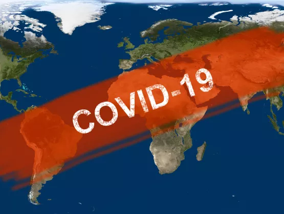
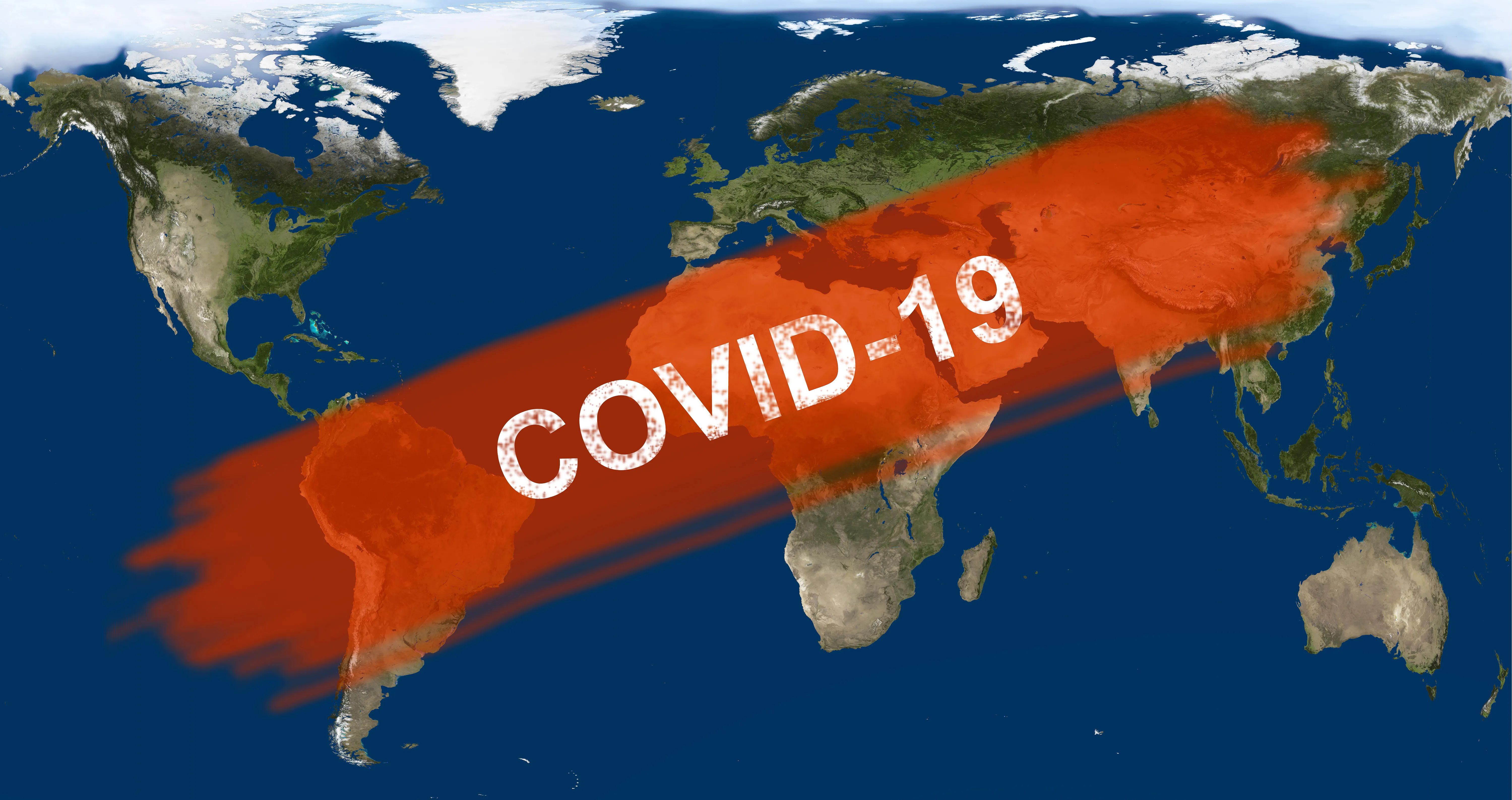
Part 1 of 2Read Part 2. While companies navigate the ongoing COVID-19 crisis, corporate leaders should be evaluating a number of key business continuity issues as well as steps they can take to not only react to business disruptions but also reshape their business and recovery plans.We spoke with Dan Steele, Senior Director and the APAC Head of Environmental, Health, Safety, and Security (EHS S) at GLOBALFOUNDRIES (GF) Singapore, via teleconference for insights into the best practices he and his team have implemented from their Business Continuity Plan (BCP) to guide them through the health crisis.SEMI: How did GLOBALFOUNDRIES Singapore first respond when the country reported its first COVID-19 case?Steele: Since the early days of our company, we have had a Business Continuity / Crisis Management (BCCM) team in place that is responsible for business continuity planning for the site. At the beginning of this journey with the coronavirus, we believed in two truths: maintaining the safety and well-being of our employees and consistently communicating precautionary measures the company has taken to protect them and our business. These actions are critical to keeping our employees safe, while keeping the anxiety level low. By informing and updating employees in a timely manner, we ensure that they are well-educated about the crisis as it unfolds and the foreseeable circumstances that could be ahead of us. Once the world was well into the coronavirus outbreak, our CEO declared in a message to all employees that “we entered this pandemic crisis together, and we will exit it together.”We have also established links to pertinent government websites and made them conveniently available to ensure employees have access to the latest available information for their personal lives.SEMI: What actions has GF Singapore taken in response to the crisis so far?Steele: On January 29, our BCCM team activated the first line of defense by initiating temperature checks at all building entrances for every individual including employees, contractors, visitors, and customers who come into our facilities. We asked each to declare their state of health and travel history and issued a temperature card to every employee and resident contractor. They are all required to record their temperature twice daily – once before coming to work and again at midday – and they present the temperature log to security upon their arrival.The following week, our teams split into an A/B work arrangement to ensure continuity of our operations. We proactively pared down our teams to the staff essential for our on-site operations, while enabling the rest to work from home. We also advised our most vulnerable employees with impaired immune systems or who are pregnant to work from home. Concurrently, we moved all meetings of 10 or more people to virtual communications and only allowed meetings with fewer than 10 to be held in rooms with participants sitting at least one meter apart. We informed our customers of our efforts and moved all planned on-site visits to online visits.In line with Singapore’s efforts to curb the spread of COVID-19 within the community, GF restricted site access of people who had recently traveled to countries with sustained community transmission and regularly updated the restriction list. To conduct contact tracing, we created our two degrees of separation list that we used to track employees with families and close associates who were linked to a COVID-19 case. Employees provided the information voluntarily. On our campus, we enforced strict safe distancing measures by limiting access to meeting rooms, marking off-limits tables and removing chairs in the cafeteria, limiting the number of elevator riders to no more than four, and placing boxes or other spacing indicators at smoking zones, bus stops and temperature-taking lines. We also initiated a daily log of employees taking the company buses tagged to the bus number, time, and employee identification numbers in anticipation of the need for contact tracing.Most recently, when the Singapore-Malaysia border closed, we activated the next phase of our BCP that was already in place – housing over 450 Malaysian employees in Singapore hotels.Throughout this crisis, we continuously monitor and evaluate possible impacts to our supply chain to ensure the continuity of our business. This is a standard element of our ongoing business continuity management system.Most importantly, we frequently communicate with our employees and tell them everything the company is doing and why we are doing it. We encouraged employees to monitor their health, stay home if they are unwell, and seek immediate medical treatment if necessary at one of our panel clinics or other medical facilities.SEMI: What are your top concerns amidst this health crisis?Steele: At GF, we are managing through the crisis with an unwavering focus on two guiding principles: the safety and well-being of our worldwide team, their families and communities; and delivering on our commitments to our clients. As the world’s leading specialty foundry, GF has a unique role in the global supply chain. Our semiconductor technology is vital to a range of industries including health care, communications, infrastructure and security. With these priorities in mind, the company undertook unprecedented steps and has adapted to the crisis by dynamically adjusting its protocols, health and safety measures, and business processes to protect its teams while maintaining manufacturing excellence.We are committed to safeguarding the well-being of our employees while supporting and sustaining our on-site operations and protecting customers’ products. A major concern is the impact on our employees. We understand that COVID-19 can be infectious even if an individual is asymptomatic – we are always concerned that temperature screening alone is not sufficient. This is the reason that from day one we have encouraged our employees to monitor their health, follow all government advice for proper hygiene and seek medical attention if unwell as early as possible, and not come to work.Dan Steele has over 25 years of experience in environmental, health and safety, and security operations. He has also held other leadership roles in facilities engineering, quality, reliability and assurance, and risk management.Bee Bee Ng is president of SEMI Southeast Asia.
Read More