downloadGroupGroupnoun_press release_995423_000000 copyGroupnoun_Feed_96767_000000Group 19noun_pictures_1817522_000000Member company iconResource item iconStore item iconGroup 19Group 19noun_Photo_2085192_000000 Copynoun_presentation_2096081_000000Group 19Group Copy 7noun_webinar_692730_000000Path
Skip to main content
Default Banner Image

cybersecurity

For years, cybersecurity in manufacturing was often treated as a mere compliance issue. Suppliers filled out questionnaires. A scan report was produced before shipment. A checklist was reviewed during qualification. A document proved that the equipment was "secure enough" at a given point in time. This model is no longer sufficient. As equipment becomes more software-driven, connected, and remotely maintained, cybersecurity responsibility is moving closer to the product itself and therefore closer to the OEM. Fabs still define their security expectations, but OEMs are increasingly expected to provide evidence that their equipment can remain secure throughout its lifecycle.Semiconductor manufacturing is entering a new phase of cybersecurity. The question is no longer simply, "Was this equipment compliant when it was delivered?" A stronger question is emerging: "Can this equipment continuously demonstrate that it is operating securely and reliably?" This shift matters because semiconductor equipment is no longer isolated machinery. It is software-intensive, networked, remotely maintained, data-producing, and deeply integrated into fab operations. Equipment controllers, factory interfaces, service laptops, recipes, logs, remote access tools, operating systems, middleware, and data acquisition services now comprise a significant digital presence surrounding the physical process. The risk is not theoretical. Industrial automation and control systems are now considered cybersecurity assets throughout their lifecycle rather than merely engineering systems. In the global semiconductor manufacturing industry, this shift is evident through the following SEMI standards:SEMI E169 provides guidance for equipment information system security. SEMI E187 defines cybersecurity requirements for fab equipment.SEMI E191 addresses cybersecurity status reporting for computing devices connected to the factory network.These semiconductor-specific standards align with the broader industrial cybersecurity trend. The ISA/IEC 62443 series addresses cybersecurity throughout the industrial automation lifecycle, including product development, integration, operation, maintenance, and supplier responsibility. The National Institute of Standards and Technology (NIST) has moved in the same direction with Cybersecurity Framework 2.0 by adding "govern" as a core function and making cybersecurity the responsibility of leadership, risk management, and the supply chain rather than just a technical activity.In Europe, this shift is also becoming regulatory. Under the Cyber Resilience Act, starting September 11, 2026, manufacturers will be required to actively report vulnerabilities and severe incidents affecting products with digital elements. They must provide an early warning within 24 hours and a full notification within 72 hours. This will encourage many industrial suppliers to strengthen their vulnerability management.A fab does not only need to know that an equipment was shipped with a supported operating system. It also needs to know if the system remains aligned with the approved configuration after installation, maintenance, remote support, patches, upgrades, troubleshooting, and years of production use.A fab needs more than a document saying that network security was considered. It needs practical evidence showing which ports are open, which services are active, which accounts exist, which software is running, and whether local protection mechanisms are still enabled. A fab does not only need supplier declarations. It needs operational proof.This is where the semiconductor industry faces a specific challenge. A fab cannot simply copy standard IT cybersecurity practices and apply them directly to production tools. The cost of disruption is too high. A patch that is harmless in an office system may affect equipment behavior, timing, qualification, or process stability. A security scan that is acceptable in IT may be intrusive in a production environment. Generic endpoint controls can create unacceptable side effects if they interfere with motion, recipes, automation, or equipment availability.Therefore, semiconductor cybersecurity must balance three constraints simultaneously:Protect the equipment and the factory network.Preserve deterministic production behavior.Generate evidence that can be trusted by fabs, suppliers, auditors, and increasingly, regulators.For this reason, the future of cybersecurity in semiconductor manufacturing will likely be built around five practical pillars.1. Secure by design, but validated in operationSecurity measures must be implemented from the outset of equipment architecture. The product baseline should include supported operating systems, hardened configurations, secure communication channels, access control, logging, and vulnerability handling. Figure 1: Equipment controllers expose trusted security context However, design is only the starting point. The equipment must also support validation after delivery. Fabs need a way to confirm that the deployed configuration still matches the secure baseline. This is especially important after field service, software updates, recipe changes, local troubleshooting, or remote maintenance. The industry is shifting from "trust me, it was secure at release" to "here is the evidence that it is still secure today."2. Cybersecurity evidence must become structured dataAll too often, cybersecurity evidence remains trapped in PDFs, spreadsheets, emails, and manual audit reports. This approach is not scalable. A modern factory needs structured, machine-readable cybersecurity information. This data does not need to be collected at the same frequency as process data, it should rather be collected at the right frequency for assurance, such as daily, weekly, after a restart or maintenance, or before a production release.This creates a strong opportunity for equipment manufacturers. The equipment controller can serve as a source of trusted security context. It can provide controlled, well-defined information about the current state of the equipment's software and configuration. This does not replace cybersecurity tools. Rather, it complements them with equipment-native context.This is important because the equipment itself knows things that external tools may not: which services are expected, which processes are part of the controller, which ports are required for automation, which accounts are intended for servicing, and which configuration belongs to the validated release.3. Communication security must move closer to the protocol layerMany industrial environments have relied on network segmentation, virtual private networks (VPNs), and perimeter controls. While these controls remain useful, they are insufficient for a Zero Trust approach.The next step is establishing stronger identities and trust between communicating systems. When equipment and factory systems exchange messages, they must know with whom they are communicating, and the communication channel must protect the confidentiality and integrity of the messages.This direction already exists in part of the semiconductor communication landscape. In EDA, also known as Interface A, SEMI E132 defines equipment client authentication and authorization, requiring clients to authenticate before further communication and enabling authorization controls for access to equipment functions and data.The same trust expectation is now emerging more visibly for SECS/GEM communication. A SEMI task force is working to secure HSMS communication, which is central to SECS/GEM-based host-equipment integration. The objective is to improve trust at the communication layer while preserving the proven behavior and interoperability that made HSMS successful in fabs.For semiconductor manufacturing, this must be done carefully. The industry cannot disrupt decades of host-equipment interoperability. The practical approach is to secure communication while maintaining existing automation behavior. This is a good example of the semiconductor cybersecurity challenge: modernizing the trust model without destabilizing the production model.4. Cybersecurity must be lifecycle-managedA semiconductor tool can remain in operation for many years. During that time, operating systems age, third-party components evolve, vulnerabilities are discovered, remote support practices change, and fab expectations become stricter. This means cybersecurity cannot be treated as a delivery milestone. It must be managed as a lifecycle capability, from design and release to installation, maintenance, upgrades, and end-of-support planning.For semiconductor OEMs, this creates a very practical challenge. They need clearer answers to questions that fabs will increasingly ask:Practical questionWhy it mattersWhat is the support status of each software component?To understand exposure to known vulnerabilities and end-of-support riskHow are vulnerabilities evaluated?To separate theoretical exposure from real equipment riskHow are patches qualified without creating regression risk?To protect cybersecurity without compromising process stability or tool availabilityHow is the customer informed?To support faster risk decisions and stronger supplier trustWhat is the fallback if a patch cannot be deployed?To define compensating measures and avoid unmanaged riskHow is the secure baseline restored after maintenance?To prevent configuration drift after service actionsHow is evidence retained?To support audits, incident response, and lifecycle traceability The answer is not simply more documentation. The answer is better evidence: structured, repeatable, and linked to the real equipment state. For semiconductor OEMs, the practical task is to convert cybersecurity requirements into evidence that fabs can verify during integration, operation, maintenance, and upgrades.Evidence categoryWhat the fab needs to knowWhy it mattersOS and software baselineSupported OS, installed components, patch statusReduces exposure to known vulnerabilitiesNetwork exposureOpen ports, active services, remote connectionsHelps detect unexpected attack surfacesAccess controlLocal accounts, roles, privilege modelLimits persistence and unauthorized accessEndpoint protectionFirewall, anti-malware, hardening statusConfirms local defenses remain activeLogs and monitoringSecurity events, configuration changes, authentication eventsSupports investigation and traceabilityMaintenance historyUpdates, remote sessions, service actionsShows what changed and whenVulnerability handlingKnown vulnerabilities, mitigation status, patch planSupports lifecycle accountability This lifecycle view is important because every change can modify the equipment security posture. A patch, a remote support session, a local service action, a new account, an opened port, or a firmware update can all move the tool away from its validated baseline. Figure 2: Cybersecurity becomes a lifecycle process This is also where upcoming regulations will change the supplier conversation. Vulnerability handling, reporting, and product security documentation will become part of business trust, not only technical trust. For semiconductor OEMs, the direction is clear: cybersecurity evidence must become part of the product lifecycle, not a separate compliance package prepared only when the customer asks for it.5. Compliance must be risk-based, not tool-prescriptiveOne of the important lessons from industrial cybersecurity is that standards and customer requirements are most effective when they specify the necessary capabilities and evidence rather than forcing every supplier to use the same tools or implementation methods. In the semiconductor industry, the SEMI Standardized Semiconductor Cyber Assessment (SSCA) is a useful example of this direction. It provides a semiconductor-specific assessment framework designed to evaluate cyber readiness and risk across the supply chain, from device manufacturers to OEMs and beyond. It also uses maturity-based questions to help assess the security posture of an organization, which supports a more risk-based view of cybersecurity capability rather than a simple pass/fail interpretation.This risk-based and maturity-based approach is also important at the equipment level. Semiconductor tools are not uniform products with identical architectures. A metrology tool, a sorter, an inspection system, an etcher, and an AMHS component may have different risk profiles, software stacks, connectivity models, and operational constraints. Even within one piece of equipment, cybersecurity responsibility is distributed across multiple layers: the main equipment controller, load ports, robots, sensors, embedded PCs, software libraries, remote access components, and third-party subsystems. The right question is not: "Did every OEM use the same scanner, report format, or internal process?" A better question is, "Can each OEM demonstrate that the equipment meets the required cybersecurity outcome, that the evidence is repeatable, and that the lifecycle process is controlled?"This question must also be addressed recursively across the supplier chain. A fab will ask the OEM for evidence. The OEM, in turn, must obtain and manage evidence from its subsystem suppliers. Those suppliers may need evidence from their own module, software, firmware, and component suppliers. In practice, cybersecurity assurance becomes a chain of trust that runs from the fab down to the lowest relevant technical layer. Figure 3: Cybersecurity assurance becomes a chain of trust The strategic direction is clear for semiconductor OEMs. Cybersecurity should be part of the equipment's value proposition. A secure equipment controller will execute more than just automation logic. It will also support secure communication, controlled access, structured logs, lifecycle traceability, vulnerability management, configuration evidence, and visibility into the security state.This is not just about reducing cyber risk. It is also about reducing integration friction with advanced fabs. It is about conducting audits more quickly. It is about limiting late-stage surprises. It is about giving customers confidence that they can operate, maintain, and upgrade the equipment without compromising factory security.The semiconductor industry is entering a phase in which cybersecurity will be judged less by static declarations and more by operational proof. That is a healthier model. Static compliance tells a fab what was once true. Operational proof shows what is true now. For semiconductor manufacturing, this distinction will become more crucial.About Dr. Fahad GolraAs Director of Product Innovation for Agileo Automation, Dr. Fahad Golra drives next-generation solutions in connectivity, data modeling, and communication architectures. Since joining the company in 2019, he has been a key force behind Agileo’s push toward Industry 4.0, championing interoperability, digital twins, and edge-to-cloud systems. With 15 years of experience spanning academia, research, and industry, Fahad brings deep technical insight and thought leadership to the semiconductor industry. An active contributor to SEMI, the Semiconductor Manufacturing Cybersecurity Consortium (SMCC) and the OPC Foundation, he is a frequent speaker at industry events and a published author advancing the dialogue around smart manufacturing and automation.
Read More
Q3 2025 was packed with activity. From finalizing the Standards program for SEMICON West, to organizing the event’s corresponding Global Standards Summit (GSS), the Standards team is excited to share its most recent quarterly developments.On Tuesday, October 7, leaders from across the industry convened in Phoenix, Arizona, for the second annual GSS. This half-day summit focused on future standardization needs for supply chain traceability and environmental sustainability. In addition, the Standards team conducted two workshops at SEMICON West. The first, SEMI Liquid Chemicals Analytical Workshop, detailed recent advances in analytical methodology and instrumentation related to particle measurement, trace metals, and organics in liquid chemicals. The second, Enhancing Voltage Sag Immunity: SEMI F47 Standards Updates Insights Workshop, offered a forum for sharing improvements to SEMI Standard F47 to further enhance tool performance and reliability. Finally, Q3 saw the official introduction of SEMI Standards T26 and E195. SEMI T26-0925, Specification for Electronic Supply Chain Traceability Using Distributed Ledger Technology, will be crucial for improving security and transparency for the industry’s supply chain. Additionally, SEMI E195-0925 is now available for purchase. This standard, Test Method Using Adhesive Replacement Substrates to Assess Particulate Surface Contamination on Critical Chamber Components, offers a testing approach for measuring the ISO 14644-9 cleanliness of a critical chamber component.To participate in upcoming standard developments, learn more about becoming a member of the SEMI International Standards Program. Global Standards Summit The SEMI GSS made its North American debut at this year’s SEMICON West in Phoenix. Building on its inaugural event at SEMICON Japan 2024, GSS is a strategic forum dedicated to creating an industry-wide standardization roadmap for the next three and seven-year benchmarks. The 2025 GSS continued conversations from SEMICON Japan on environmental sustainability, while expanding its program to include supply chain traceability. As geopolitical tensions, mounting cybersecurity threats, and rising technological demands continue testing the limits of the industry’s supply chain, the need for global standardization is becoming increasingly apparent. The 2025 GSS program addressed these concerns and others across multiple sessions, offering insight on how these challenges are being addressed in the industry while highlighting critical areas still in need for standards development. Key outcomes from the GSS program include: Addressing data sharing across multiple supply chain tiers while protecting IP rights and a call for harmonization across standards. The presentation by Randy Hall from the Provenance Chain Network, offered approaches on how data owners can share information with authorized users without compromising sensitive manufacturing details. While there are standards gaps that hinder broader adoption, there is opportunity to address insufficient visibility across the industry’s supply chain amid ongoing cybersecurity threats by harmonizing across existing standards implementations. An integrated modeling framework for informing energy efficiency and carbon reduction approaches. Developed by the International Roadmap for Devices and Systems (IRDS) Environmental Sustainability for Semiconductor Facilities (ESSF) team, this effort helps address demands for maintaining rapid technological progress while still meeting the industry’s ambitious sustainability goals.Standardization opportunities for improving sustainability within manufacturing facilities. Nate Monosoff from Jacobs offered insight into the decision-making tradeoffs that balance sustainability with other facility performance areas, focusing on standard methods for calculating ESG performance. GSS concluded with a panel discussion that featured leaders from AMD, FTD Solutions, Intel, The Provenance Chain Network, Jacobs, Qualcomm, and Tokyo Electron. In this session, our thought leaders discussed the fundamental importance of standardization for our industry, standards adoption, incentivizing stakeholders, and how standards can be designed to remain flexible and adaptive as technologies and regulatory landscapes evolve. SEMI Standard T26In line with the 2025 GSS theme of supply chain traceability, the Standards team is pleased to introduce SEMI T26, Specification for Electronic Supply Chain Traceability Using Distributed Ledger Technology. This standard was published in September to define a secure and decentralized traceability system that all members of the electronics supply chain can safely share. This system is based on distributed ledger technology to improve industry-wide reliability assurance.Update on Document 7130CIn February, Document 7130C was approved during the North America Metrics Technical Committee Chapter Meeting. The document officially became SEMI E195 - Test Method Using Adhesive Replacement Substrates to Assess Particulate Surface Contamination of Critical Chamber Components in September.SEMI E195 describes a quantitative method for measuring the ISO 14644-9 surface cleanliness for particle concentration of a critical chamber component (CCC), by means of an adhesive replacement substrate. The purpose of this standard is to ensure measuring and reporting consistency across CCCs or processing equipment manufacturers. To help acquaint the industry with this standard, SEMI offered a combined, in-person course on SEMI E194 and SEMI E195 during SEMICON West. The course provided fundamental information on each standard, in addition to other process approaches for improving reliability and yield.Other SEMI Updates:SEMI Preventive Maintenance Automation White Paper SEMI Korea conducted a Global PM Automation Survey in August to better understand today’s preventive maintenance readiness issues for autonomous fabs. The results will be included in SEMI’s upcoming PM Automation Whitepaper and will ultimately guide future developments for related SEMI Standards. Standardized Semiconductor Cyber Assessment FrameworkIn Q3, the Semiconductor Manufacturing Cybersecurity Consortium (SMCC) released its Standardized Semiconductor Cyber Assessment (SSCA) framework. This document provides a detailed cybersecurity readiness plan for semiconductor companies across the supply chain. Its goals are to standardize industry-wide cybersecurity risk evaluations, establish and accelerate the adoption of best practices, and improve information sharing and collaboration. Download the SSCA framework for free.New Data Standard for Equipment Edge Governance In June, Document 6938C was approved during the Taiwan Information Control Technical Committee Chapter Meeting. The document officially became SEMI E196 - Guide for Equipment Edge Data Governance. SEMI E196 provides guidance for identifying equipment data supplied by manufacturers that can be used in equipment engineering or analysis applications.New Guide to Meet IRDS Yield Table RecommendationsAt the NA Summer Meetings, Document 6601B passed TC Chapter review with technical changes and a Ratification Ballot was issued in Cycle 7-2025. Pending final Procedural Review, Guide for Meeting IRDS Yield Table Recommendations for High Purity Polymer Materials and Components Used in Ultrapure Water, will cover areas that establish criteria for allowable contribution by critical components used for UPW treatment plant and distribution system. This document will be proactively updated to manage the risks associated with the high purity polymer materials used in the semiconductor process. The biggest challenges today are metals and particles and certain organics.Flex Standards Meeting at FLEX 2026Meet the leaders of the SEMI Standards Flexible Hybrid Electronics (FHE) Task Forces at Flex 2026, in Arizona, February 24-26, and learn about ongoing FHE standardization efforts!Standards Introduced in Q3 2025New and revised standards released in Q3. July 2025 StandardsAugust 2025 StandardsSeptember 2025 Standards Get InvolvedSEMI Standards development activities take place throughout the year in all major manufacturing regions. To participate, join the SEMI International Standards Program.SEMI Standards are available through individual download purchases or online via SEMIViews. Sign up for a 30-day SEMIViews trial.For more information, please visit the Standards website and events page. For any questions regarding SEMI Standards activities, please contact your local SEMI Standards staff. Paul Trio is Director of Standards at SEMI.
Read More
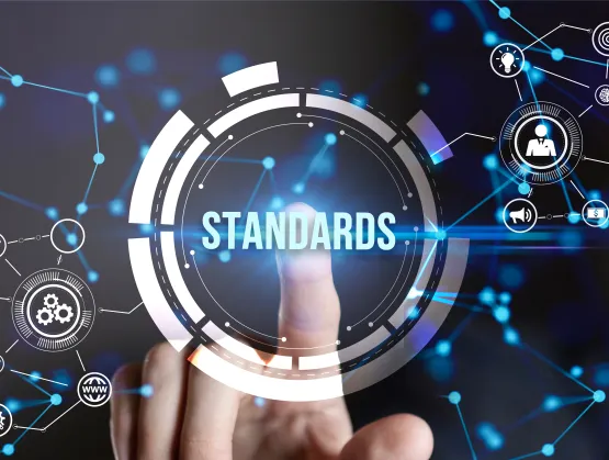
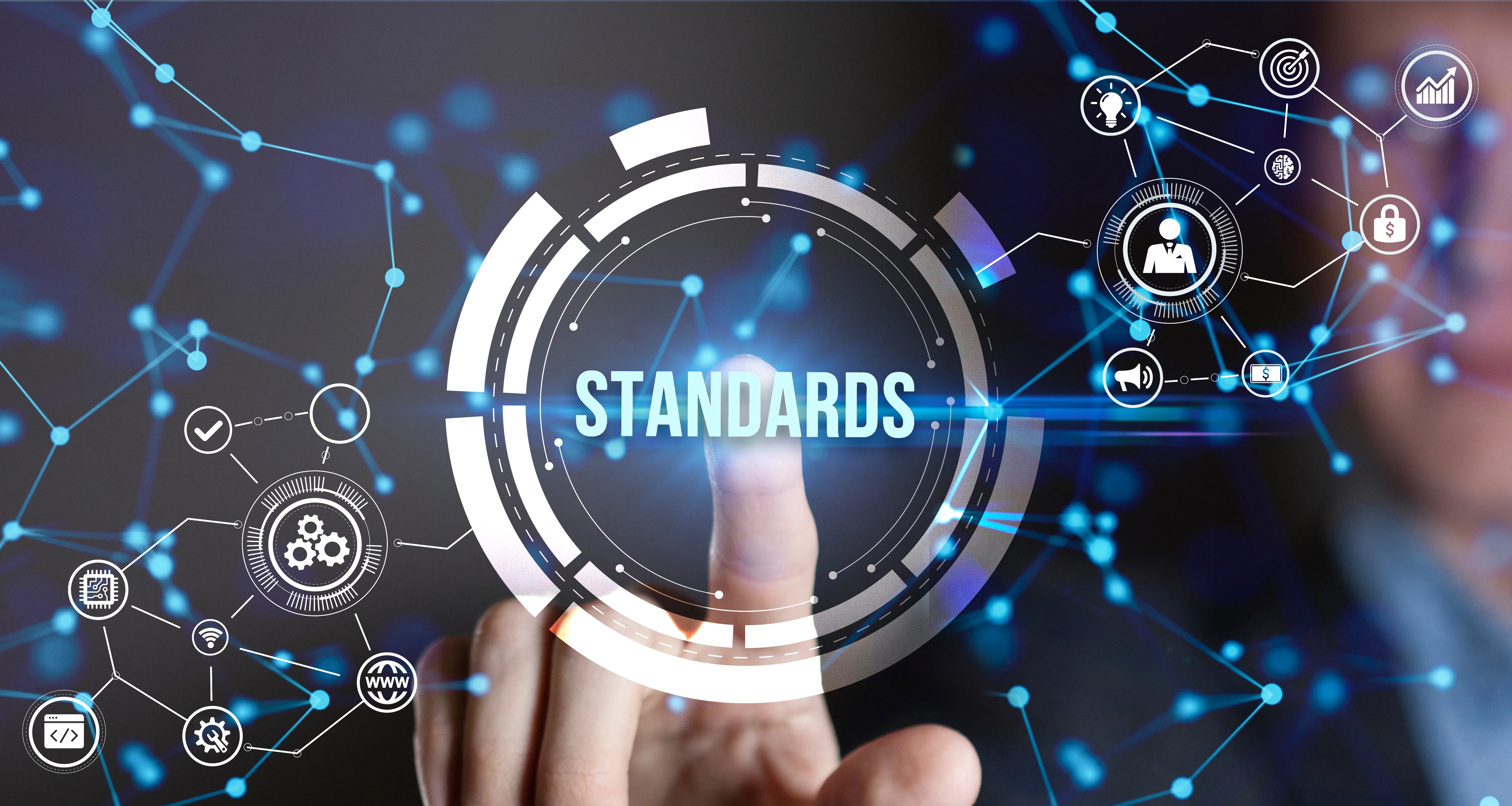
In Q2, the SEMI International Standards Program made progress on several emerging initiatives. Together, we reached a critical milestone for one of our data standards initiatives with Document 6938C recently passing Technical Committee review in mid-June 2025. Ballot 6938C, which provides guidance on how to identify manufacturing equipment data provided by the equipment supplier that can be used in equipment engineering or analysis applications, is slated to join SEMI E190 and E190.1 in providing industry-enabling data standardization.In addition, we began major revisions to SEMI Standards S2, S8, and S10. These standards govern environmental, health, and safety (EHS) considerations, equipment user fatigue and injury reduction, and equipment risk assessment and evaluation, respectively. In our recently concluded North America Standards Summer 2025 Meetings, the NA EHS Technical Committee Chapter approved a revision ballot to SEMI S10. The ballot (7169) proposed several major revisions to the SEMI S10 Safety Guideline on risk assessment which included changes to references to equipment to objects under consideration. Other changes also included the relocation of the assessment of the risk of harm to property other than the OUC to a Related Information section. Additional details are provided below.We’re eagerly preparing for this year’s SEMICON West event, taking place for the first time ever in Phoenix, Arizona. We are also pleased to announce the return of the SEMI Global Standards Summit taking place Tuesday afternoon, October 7 at SEMICON West. Our inaugural Summit was held last year at SEMICON Japan 2024 last December. The Summit aims to identify standards-critical areas and work towards an industry standardization strategy for the next 3- and 7-year time horizons. This year's Global Standards Summit will feature sessions on Supply Chain Traceability as well as Environmental Sustainability. Similarly, as cybersecurity considerations become more complex, SEMICON West will host a dedicated Cybersecurity Forum from October 7-9 to address today’s most pertinent challenges. More detailed program information will be available soon. Finally, we’re looking forward to our SEMI Standards + Award Ceremony Networking Event at SEMICON West. Following the International Standards Meeting and Standards Summit on Tuesday, October 7, join us for appetizers, drinks, and great conversation from 6-7:30 p.m. In the meantime, learn more about becoming a member of the SEMI International Standards Program.Balloting for Document 6938Document 6938C introduces a new potential standard – Guide for Equipment Edge Data Governance. Under development by the Equipment Edge Data Governance (EEDG) Task Force since 2021, Document 6938C was balloted in Cycle 3-2025 and approved during the Information Control Taiwan Technical Committee (TC) Chapter meeting held on June 12, 2025. It has since received approval by the International Standards Committee Audits and Reviews Subcommittee and is now undergoing final processing for publication by SEMI. As manufacturing equipment offers more accessible data than ever, poor communication, inconsistent expectations, and data security concerns continue to halt or slow factory integration efforts. If passed, this new standard will help organize the information that supports smart manufacturing efforts at the edge. In addition, the EEDG Guide will provide a comprehensive set of best practices to both users and suppliers to increase the value of existing equipment data. Update on Revisions to SEMI S2, S8, and S10 Safety GuidelinesOur 2025 Q1 Standards Watch newsletter announced a significant overhaul for SEMI Standards S2, S8, and S10.S2, SEMI’s standard for performance-based environmental, health, and safety (EHS) considerations for semiconductor manufacturing equipment, is undergoing discussions on redefining safety interlock systems. The S2 task force will issue an informal ballot to the general audience for feedback. The results then will be used to develop a formal letter ballot.First developed in 1995, SEMI Standard S8 works to reduce fatigue and injury by matching equipment to the user’s size, strength, and range of motion. Although this safety standard has been periodically updated since its inception, its last substantial revision was in 2018. The ballot to revise S8 ultimately failed the EH S TC Chapter review at this year’s Winter Meeting. With 214 comments and negatives to consider, the task force is revising the ballot and plans to reissue in Cycle 7 of August 2025.Finally, SEMI Standard S10 is moving through ballot 7169. This standard defines a consistent means of risk estimation that other SEMI Safety Guidelines can invoke. Ballot 7169 will separate facility and building risk assessment to a non-normative portion of the document, ensure EHS risks are separately calculated from commercial object risks, and clarify risk assessment of observed events from risk assessment of foreseen events. Ballot 7169 results were reviewed on June 5 during the North America Standards Summer meetings. The document was approved and is being processed for publication by SEMI.Cybersecurity Forum at SEMICON West 2025This year’s SEMICON West will feature a dedicated Cybersecurity Forum to address the semiconductor industry’s rapidly-changing cybersecurity landscape. The SEMI Cybersecurity Forum will gather industry experts to share knowledge and experience on the following topics. The goal is to develop actionable strategies and a deeper understanding of current and future cybersecurity risks. Cybersecurity in Legacy Semiconductor ToolsEmerging and Existing Cybersecurity Legislation and ComplianceCybersecurity in Maintenance and ManufacturingImpact of Cybersecurity Events on Semiconductor Manufacturing OperationsSupply Chain SecurityThreat Landscape in Semiconductor ManufacturingThe 2025 call for abstracts is now closed. Speakers will be announced in Q3.SEMI E187 Compliance Guidance White PaperThe SEMI Semiconductor Manufacturing Cybersecurity Consortium (SMCC), in collaboration with industry experts, is pleased to announce the release of the SEMI E187 Compliance Guidance Whitepaper. This comprehensive resource is designed to support semiconductor equipment suppliers and device manufacturers as they work to meet the requirements of the SEMI E187 0122 Standard - The Specification of Cybersecurity of Fab Equipment.Professionals involved in tool development, manufacturing, operations, and security will find the guidance particularly relevant and actionable. It provides guidance to address all twelve SEMI E187 requirements and focuses on new to fab equipment.Download the Whitepaper for freeSEMI Standards North America Summer MeetingsThis year’s SEMI Standards North America Summer Meetings were held from June 2-5 at SEMI’s headquarters in Milpitas, California. The meetings convened 11 committees and 40 task forces to discuss topics ranging from EHS to facilities, 3D packaging, MEMS, and more. In addition to the results of ballot 7169, technical changes to ballot 6601B, New Standard: Guide for Meeting IRDS Yield Table Recommendations for High Purity Polymer Materials and Components Used in Ultrapure Water, was also approved by the Liquid Chemicals North America TC Chapter, since the activity began in 2019. A Ratification Ballot will be issued in Cycle 7-2025 to verify the changes. In total, over 15 activities, ranging from Auxiliary Information, Reapprovals, and Line-Item ballots, also recently passed Procedural Review by the International Standards Committee (ISC) Audits Reviews Subcommittee and will be forwarded to Publications for final processing. The next SEMI International Standards Meeting will be held at SEMICON West from October 7-9 at the Phoenix Convention Center. Some technical committees and task forces may meet virtually outside of this meeting set, so be sure to check the SEMI Standards calendar of events for updates. Standards Introduced in Q2 2025New and revised standards released in Q2. April 2025 standards: https://store-us.semi.org/collections/standards/stdpbc-0425May 2025 standards: https://store-us.semi.org/collections/standards/stdpbc-0525June 2025 standards: https://store-us.semi.org/collections/standards/stdpbc-0625Get InvolvedSEMI Standards development activities take place throughout the year in all major manufacturing regions. To participate, join the SEMI International Standards Program.SEMI Standards are available through individual download purchases or online via SEMIViews. Sign up for a 30-day SEMIViews trial.For more information, please visit the Standards website and events page. For any questions regarding SEMI Standards activities, please contact your local SEMI Standards staff. Paul Trio is Director of Standards at SEMI.
Read More
With microelectronics manufacturing increasing in complexity and facing more cybersecurity threats, the SEMI International Standards Program has made crucial progress on efforts to address these challenges and others, in the first quarter of 2025. MEMS manufacturing readiness and cybersecurity came into sharp focus with the introduction of SEMI Standard MS15 - Guide to MEMS Manufacturing Readiness Levels. In addition, this quarter saw the opening of the public commentary period for a SEMI-led semiconductor manufacturing cybersecurity profile, developed for the National Institute of Standards and Technology’s (NIST) Cybersecurity Framework (CSF) 2.0. Through collaborative efforts, we held a successful North America Standards Winter Meeting in February, co-hosted a MEMS webinar, and published over 15 new and revised standards in areas such as equipment automation software, facilities, materials, and more.With exciting developments still to come, we’re looking forward to a wonderful year ahead.MEMS Manufacturing Readiness This March, SEMI unveiled its new standard, SEMI MS15 – Guide to MEMS Manufacturing Readiness Levels. This standard offers readiness level definitions, processes, and practices for creating MEMS products that meet targeted specification performance, quality, cost, and time-to-market. This standard is broken into eight distinct levels that cover basic research, all the way through high-volume production. Prior to the official release of SEMI MS15, we held a webinar that previewed how MEMS Manufacturing Readiness Levels will facilitate efficient MEMS development. Led by co-chair, Michelle Bourke of Lam Research, the SEMI MEMS Sensors Industry Group (MSIG) hosted a webinar featuring MEMS experts from SoftMEMS, HP, Teledyne MEMS, and Polar Semiconductor. Speakers shared insight into creating a structured and balanced MEMS manufacturing approach to drive successful products to commercialization. Cybersecurity Resilience Like 2024, cybersecurity remains pertinent in 2025. Last October, SEMI introduced SEMI Standard E191 and its subordinate standard, SEMI E191.1 to help define cybersecurity status information reporting. SEMI E191 and E191.1 join SEMI’s existing cybersecurity standards, SEMI E187 and E188. Last year also saw the development of the NIST CSF 2.0 Semiconductor Manufacturing Profile under SEMI’s Semiconductor Manufacturing Cybersecurity Consortium (SMCC). In partnership with NIST, SMCC advanced a community profile for CSF 2.0 that will serve as a cybersecurity framework specific to semiconductor manufacturing. The profile opened for public commentary between February 27 and May 30, with the final version slated for official release in Q3 of this year.As the semiconductor industry becomes increasingly reliant on digital technologies, we will continue to prioritize cybersecurity standards and initiatives essential for safeguarding the global supply chain.North America SEMI Standards Winter MeetingsFrom February 24 to 27 at SEMI’s headquarters, leaders from 11 committees and over 40 task forces collaborated on new and revised standards and safety guidelines for environmental, health, and safety, equipment automation and software, liquid chemicals, traceability, and more. Three SEMI Standard draft documents that were reviewed at the North America SEMI Standards Fall Meetings last November have also been approved and published. In addition to SEMI MS15, SEMI F122 – Guide for Facilities Data Package for Manufacturing Equipment Installation and Building Information Modeling, and SEMI E193 – Specification for 300 mm Film Frame FOUP (FFF), have also been approved and published. SEMI F122 suggests formats for reporting facilities data required to plan, prepare, model, and optimize a facility for the installation of manufacturing equipment by fab owners and manufacturing equipment customers. SEMI E193 drives consistent implementation of interfaces for film frame carriers that are compact and work with existing 300 mm FOUP standards and BOLTS interfaces. These standards are now available for purchase. The North America SEMI Standards Summer Meetings will take place from June 2-5 at SEMI’s Milpitas, California headquarters. Some technical committees and task forces may meet virtually outside of this meeting set – check the SEMI Standards calendar of events for updates!Standards Introduced in Q1 2025New and revised standards released in Q1. January 2025 standards: https://store-us.semi.org/collections/standards/lang-english+stdpbc-0125February 2025 standards: https://store-us.semi.org/collections/standards/lang-english+stdpbc-0225March 2025 standards: https://store-us.semi.org/collections/standards/lang-english+stdpbc-0325TestimonialsHear from Doug Suerich, Director of Marketing at PEER Group, how his work is helping shape smart manufacturing standards and global cybersecurity policies through our powerful collaborative platform. Get InvolvedSEMI Standards development activities take place throughout the year in all major manufacturing regions. To participate, join the SEMI International Standards Program.SEMI Standards are available through Individual Download purchases or online via SEMIViews. Sign up for a 30-day SEMIViews trial.For more information, please visit the Standards website and events page. For any questions regarding SEMI Standards activities, please contact your local SEMI Standards staff. Paul Trio is Director of Standards at SEMI.
Read More
In an era where technology permeates every aspect of our lives, the semiconductor industry serves as the backbone of innovation. From IoT devices to data centers, every piece of technology relies on integrated circuits (ICs) such as intellectual property (IP) cores and system on chips (SoCs). As these technologies become increasingly pervasive, the importance of hardware security assurance in the design and development of IP and SoCs cannot be overstated. Evolving cyber threats and sophisticated attacks make it essential for vendors to integrate advanced security measures into their workflows.Market Pressures Driving Demand for Enhanced Hardware Security The semiconductor market is projected to reach $1 trillion by 2030. At the same time, semiconductor devices and system designs are becoming increasingly complex. With that complexity comes the added difficulty and effort required to conduct thorough security analyses. Additionally, competitive pressure to reduce time-to-market means that vulnerabilities can be more easily overlooked or exploited, making it crucial for the industry to adopt automated security solutions. As more products are deployed in critical systems, from consumer electronics to national infrastructure, the stakes become even higher, underscoring the necessity for robust security measures.According to the SEMI Electronic Design Market Data (EDMD) report, in 2023, the electronic design automation (EDA), semiconductor IP, and related services market reached $17.1 billion, fueled by the increasing complexity of semiconductor designs and the growing emphasis on security. While the overall EDA market is growing at a 7.4% compound annual growth rate (CAGR), the semiconductor IP segment is expanding at 9.7%, and in comparison, the logic verification tools market alone is surging ahead at 24.2%. Deeper verification processes and tools are needed to not only handle the rising complexity of semiconductor designs, but also to support the growing emphasis on secure-by-design principles to ensure robust and reliable products in an evolving technological, security, and threat landscape. As a result, the market for logic verification tools — a key component of the EDA market — is surging. The Rising Cost of Cyber Threats from Data Breaches and Architectural Flaws Pavani Jella, Silicon AssuranceThe average cost of a data breach is $4.88 million1, encompassing lost business, regulatory fines, legal fees, and damage to brand reputation. As the semiconductor market grows, the potential financial impact of security breaches due to hardware vulnerabilities also escalates. Companies must invest in robust security measures to mitigate these risks and protect their financial health.Cyber threats from the exploitation of architectural flaws are another threat. Plundervolt is one example of an architectural flaw that could lead to hardware exploitation. Discovered by ethical hackers, Plundervolt is the name of an attack that exploited voltage fault injection to compromise the security of Intel processors. By manipulating the voltage supplied to the CPU cores, attackers could induce errors in the SGX enclave, allowing them to leak sensitive data or even bypass security protections intended by the enclave. This flaw was particularly concerning because it operated at the hardware level, making traditional software security measures ineffective. The attack leveraged the SoCs’ power management features, specifically dynamic voltage and frequency scaling (DVFS), to achieve its malicious objectives.Exploiting such a vulnerability could lead to the exposure of sensitive data, such as cryptographic keys and proprietary information, compromising the confidentiality of secure enclaves. This breach could erode trust in an IP or SoC provider’s security features, particularly in environments that rely on using the IP or SoC for protecting critical data. In cloud environments, a successful exploit could result in multi-tenant data breaches, impacting numerous users.The vulnerability also poses risks to secure applications, potentially leading to manipulated outcomes and decrypted communications. Businesses could face significant financial losses, operational disruptions, and regulatory consequences due to such an attack. It is a stark reminder of how architectural flaws in SoCs can be exploited, leading to severe security breaches that are challenging to mitigate without hardware-level fixes.Industry Believes Hardware Security Assurance Is a Key Priority A majority of security professionals from a diverse group across industry, defense, government, and academia rate hardware Trojan detection, IP piracy protection, and SoC vulnerability assessment as high priorities. This prioritization reflects the industry's awareness of the critical importance of security measures in maintaining the integrity and reliability of semiconductor products.As a result of this awareness, investments in cybersecurity are expected to reach $345.4 billion by 2026, growing at a CAGR of 9.7%2. This substantial investment demonstrates the global commitment to enhancing security measures across all industries, including semiconductors, to combat the escalating threat landscape.New EDA Tools and Investments Needed to Combat Cyber Threats The adoption of new EDA solutions is essential, despite the initial costs. Costs can range from $100,000 to $1 million per license for general EDA design and verification tools, depending on the complexity and capabilities of the software. Pre-silicon security EDA tools can detect vulnerabilities early in the design phase, significantly reducing the risk of exploitation and the need for costly post-production fixes while enhancing product reliability. Secure-by-design principles ensure that security measures are integrated throughout the development process, rather than added as afterthoughts.Integrating these new tools also requires investment in training and potential adjustments to existing workflows. However, the improved security and efficiency provided by these tools can offset these initial costs.While the costs of acquiring advanced EDA tools and deploying them in the workflow is significant, the investment is justified by the long-term benefits of enhanced security and reduced risk of costly breaches. Secure-by-design practices can prevent significant financial losses from security breaches, offering substantial long-term savings. Companies that invest in robust security measures are better positioned to demonstrate market leadership and build customer trust and loyalty, while avoiding the reputational and financial damage associated with breaches.ConclusionThe semiconductor industry is at a critical juncture where the application of advanced EDA solutions for hardware security is not just beneficial, but essential. The time to act is now.The increasing sophistication of cyber threats and the financial repercussions of security breaches make it imperative for IP and SoC vendors to adopt advanced EDA security assurance solutions to secure their designs. By investing in cutting-edge EDA tools and prioritizing security from the earliest stages of design, vendors can safeguard their products, maintain market competitiveness, and protect against the ever-evolving landscape of cyber threats.References1. IBM Cost of a Data Breach Report 20242. KPMG 2024 Global Semiconductor Industry OutlookPavani Jella is the Vice President of Business Development at Silicon Assurance, a member of the Electronic System Design Alliance (ESDA) a SEMI Technology Community. Silicon Assurance specializes in hardware security assurance solutions. With a strong background in the semiconductor and EDA industries, Pavani plays a pivotal role in driving strategic growth and fostering innovative partnerships. Passionate about the intersection of technology and security, she helps organizations adopt state-of-the-art solutions that ensure the resilience and trustworthiness of their hardware systems.
Read More