downloadGroupGroupnoun_press release_995423_000000 copyGroupnoun_Feed_96767_000000Group 19noun_pictures_1817522_000000Member company iconResource item iconStore item iconGroup 19Group 19noun_Photo_2085192_000000 Copynoun_presentation_2096081_000000Group 19Group Copy 7noun_webinar_692730_000000Path
Skip to main content
Default Banner Image

sensors

Air pollution is one of the grand challenges facing the entire planet — from the wealthiest nations to the least developed. The World Health Organization reports that nine out of 10 people breathe air containing high levels of pollutants, and that polluted air takes over seven million lives annually through stroke, heart disease and respiratory ailments.As a result, the world is thirsty for reliable, high-performing chemical and environmental sensors that can provide previously unavailable real-time awareness of environmental conditions. On one level, this seems like a relatively simple step, given that smartphones are already equipped with miniaturized sensing technologies that can monitor our living environment and activities.While highly desirable, embedding air pollution sensors in common mobile and wearable devices has not been feasible previously because the necessary trade-offs between high performance and miniaturization have made it impossible.This situation drove a CEA-Leti team to develop a novel generation of fully integrated optical chemical sensors that leverage MEMS technologies. The team successfully merged multiple functionalities on the same chip, using integrated optics and photonics, fluidics, acoustics and electromechanical transduction. How did the team overcome significant technical obstacles to design a proof-of-concept device that senses multiple environmental pollutants — housed in a minimal hardware footprint?Advancing Chemical Sensor Capabilities with Silicon Featuring high selectivity, real-time performance, and fully reversible capabilities, optical chemical sensors are perfect candidates for industrial, environmental and biomedical applications. Consequently, in recent years, worldwide R D initiatives have invested substantial effort to improve them.R D programs have focused particularly on the mid-infrared (Mid-IR) wavelength range (2.5 - 12 µm) — also known as the molecule fingerprint region, which provides a unique combination of fundamental absorption order-of-magnitude bands and unambiguous identification of specific chemicals. A multitude of molecules generate strong and distinct absorption lines in the Mid-IR, providing a foundation for accurate spectroscopic detection. Traditionally, however, these sensors have required large and expensive lenses for infrared (IR) light, making them too big and costly for resource-constrained wearables and mobile devices.Fortunately, recent advances in integrated silicon photonics and quantum cascade laser (QCL) technologies have spurred investigation of new chemical sensor architectures. Richard Soref, a research professor at the University of Massachusetts Boston’s department of engineering, introduced the extension of Near-IR technology into the longer-wave Mid-IR infrared region in 2006. Soref’s concept showed that highly sensitive and selective gas sensors could be fabricated on planar substrates at low cost by co-integrating silicon MEMS, group IV photonics, and specifically designed III-V hetero-structures.While this approach showed promise, it preceded the widespread availability of most mobile devices and wearables. Foreseeing today’s proliferation of those devices, CEA-Leti developed the different building blocks required to implement these concepts in real devices.A New Concept of Integrated OpticsLeveraging these interesting findings, the institute developed a new combination of integrated optics and multiple sensor functions on a single chip: QCL sources, a photo-acoustic (PA) cell, and a mid-IR photonic integrated circuit (PIC) combiner. Their integration on a planar substrate (Figure 1) helped to achieve higher performance, new capabilities, and higher reliability at lower cost, all in a smaller package (less than a 1 cm3 or smaller than a 1-cent coin) with reduced weight and power consumption (less than 100 mJ per measurement). Figure 1: Fully integrated optical sensor (Courtesy: CEA Leti) This configuration represents a multi-gas-detection enabler. The PIC replaces costly, fragile discrete optics while the PA detector uses a MEMS microphone to replace bulky multi-pass cells.PA spectroscopy is among the most sensitive techniques available for monitoring chemical emissions or detecting gas traces. It relies on excitation of the chemical with a pulsed light source emitting at the absorption wavelengths of such molecules. The relaxation process creates local periodic variations of the temperature, resulting in stationary pressure waves, which high-performance microphones can detect.This new generation of devices, fully fabricated on silicon, shows performance comparable with state-of-the-art systems, with the huge bonus of small size and power efficiency that work well for mobile and wearable electronics. By supporting integration onto common technological platforms, such as on-chip photoacoustic sensors, researchers have successfully realized these miniaturized and cost-effective Mid-IR photonic devices in silicon. Mobile device and wearables manufacturers can now take advantage of manufacturable integrated devices for applications that are highly sensitive to size, performance and cost. Adding gas sensing to mobile devices and wearables is now very feasible.For more information on chemical sensing at CEA-Leti, please visit or contact: http://www.leti-cea.com/cea-tech/leti/englishCEA-Leti is an active member of SEMI-MEMS Sensors Industry Group. The technology research institute, along with Fraunhofer and imec, recently joined SEMI’s family as a Strategic Association Partner under a memorandum of understanding (MOU). Under this agreement, CEA-Leti will work with SEMI to advance technology roadmaps, industry standards and cutting-edge technologies including Internet of Things (IoT), artificial intelligence (AI) and machine learning that enable new capabilities across healthcare, automotive and other electronics manufacturing ecosystems. Sergio Nicoletti has more than 20 years of experience in micro and nanofabrication, including magnetic, superconducting and chemical sensing devices and technologies. Having joined CEA-Leti in 2006 as project manager for optical sensing devices used in chemical detection, Nicoletti is currently business development manager at the institute.Previous positions include research and project management at CNR-IMM (Bologna, Italy) and at Hitachi Global Storage Technologies. Nicoletti was also a visiting scientist at HGST (San Jose, Calif.), where he worked on magnetic recording-head devices.Nicoletti holds more than 20 patents and has more than 70 publications in peer-reviewed journals. In 2016, he was appointed coordinator of the European H2020 project MIRPHAB and is director of the project’s pilot line.Nicoletti received his Ph.D. in physics, with a focus on HTc superconducting devices, from Université Joseph Fourier (Grenoble, France). References“Photoacoustic cell on silicon for mid-infrared QCL-based spectroscopic analysis,” JG Coutard, A Glière, JM Fedeli, O Lartigue, J Skubich, G Aoust, A Teulle, T Strahl, S Nicoletti, M Carras, L Duraffourg. Proceedings Volume 10931, MOEMS and Miniaturized Systems XVIII; 109310V (2019) https://doi.org/10.1117/12.2506514“Miniaturization of mid-IR sensors on Si: challenges and perspectives,” S Nicoletti, JM Fédéli, M Fournier, P Labeye, P Barritault, A Marchant, A Glière, A Teulle, J Coutard, L Duraffourg - Silicon Proceedings Volume 10923, Silicon Photonics XIV; 109230H (2019) https://doi.org/10.1117/12.2506759
Read More
New MEMS-based products are constantly emerging, fueled by the Internet of Things (IoT), autonomous driving, smart manufacturing and healthcare applications. The MEMS pressure sensor market is no exception to this trend1. Its growth has been driven mainly by automotive applications such as tire pressure management system (TPMS) regulations in China, fuel and ignition systems, thermal systems, oil-pressure monitoring, and indoor and outdoor navigation systems. Easy to customize and integrate, miniature, sensitive, accurate and low-power MEMS devices are especially well-suited to the accuracy, power consumption, sensitivity and miniaturization that pressure sensors require.Yet MEMS design also presents some specialized challenges, such as a strong coupling between fabrication technology and design. Complex physical structures that exhibit non-linear behavior, custom packaging requirements, and a final product that requires integration with surrounding CMOS circuitry are just a few examples. What’s more, there is a lack of standardized processes and process validation in MEMS design ecosystems. Pressure Sensor (Courtesy: X-FAB) As with other products based on MEMS technology, designers must increasingly customize pressure sensors for higher performance – sensitivity and linearity, in this case – while decreasing their package size. Designers can accomplish the task by studying sensor performance and manufacturability using computer models prior to fabrication. This can ensure that the sensor meets its required specifications while simultaneously reducing manufacturing cycles and cost.The Power of CollaborationThis is where strong collaboration among EDA providers, MEMS technologists and designers delivers tangible benefits. EDA providers and MEMS foundries can collectively help MEMS designers to incorporate foundry process constraints into their designs.In the semiconductor industry, first-pass successful silicon relies on standardized manufacturing processes, thorough technology characterization, accurate model generation, established simulation and verification, and extensive reuse of proven design blocks. In the MEMS world, where processes and products are developed concurrently, and processes change with every product, is it possible to adopt standardized processes, design methodologies, and tools that enable efficient reuse of existing technology and design knowledge? The challenge lies in maintaining the flexibility to optimize products for a diverse array of requirements. The ideal design platform should ease sharing of technology and design data between the foundry and its customers, enabling two-way collaborative development and allowing foundry technologists to easily perform a feasibility assessment of a customer’s project. This approach offers important benefits, allowing designers to explore and evaluate the suitability of a foundry’s process technology in their unique application. It also supports accurate prediction of device performance prior to fabrication and reduces costly build-and-test cycles. Combining standardized manufacturing processes, MEMS process design kits (PDKs), and a proven design flow are the starting point for development of manufacturing-ready designs.A Real-Life Example using Pressure SensorsAn EDA company, Coventor (a Lam Research company), along with MEMS foundry partner X-FAB, collaborated to develop a PDK that would ensure that manufacturing constraints are automatically considered early in their design process. The design flow is based upon an X-FAB fabrication platform that supports multiple process options for the manufacturing of absolute and relative MEMS pressure sensors. The PDK is a “golden container” for all the process and material characteristics of the silicon membrane and substrate, glass, passivation layers, and piezoresistive components. It enforces material properties and guarantees their correct implementation during the simulation. It also includes a component library containing ready-to-use, 3D parameterized devices (such as membranes and resistors), all pre-designed with foundry-supported materials to support their respective design rules. The components are readily partitioned for optimized meshing and simulation, saving design and simulation time. Figure 1: The elements and design flow of the PDK designed by Coventor and X-FAB. (Courtesy: Coventor)Designers can use components from the library to create a custom design — which might include different membrane shapes and sizes, and resistors of varying shape, size and position — to simulate the impact of different technology variants (such as resistor doping profiles, membrane and substrate thickness, glass material properties, and passivation schemes). This allows them to anticipate the effect of these design changes on sensor sensitivity for varying pressure and temperature regimes.Extensive validation of the pressure sensor design platform is currently underway. So far, the simulations have exhibited very good correlation to actual device measurements across a range of pressure and temperature conditions, including predictions of non-linear behavior for various pressure sensor designs. At the same time, the simulation accounts for mechanical membrane properties and piezoresistivity. With this type of design platform, a foundry can provide guidelines to help customers select both the fab technology and design features that lead to an optimal design solution. Figure 2: Simulation results depicting mechanical displacement in a pressure sensor design (Courtesy: X-FAB) Let’s Face the Next Challenges…A complete design platform for MEMS must eventually include not only MEMS device design, but system integration functions, such as the application-specific integrated circuit (ASIC) design and packaging/assembly of the product. In addition to the design verification that the PDK provides, additional partnerships among foundries, integrated device manufacturers (IDMs), research centers, equipment suppliers, and EDA vendors will help to define requirements and solutions that address every level of design and production. These might include tasks such as describing standardized material properties and process specifications, creating accurate foundry-proven design models, and defining requirements for system-level simulation. In the future, PDK simulations might even include up to tape-out and physical verification. To learn more about this collaborative PDK development work, please click here for the whitepaper.Christine Dufour, MEMS PDK Program Manager, CoventorChristine Dufour is the MEMS PDK program manager at Coventor. She has more than 20 years of experience in the semiconductor industry, leading process design kit development for BiCMOS and CMOS processes at several major semiconductor companies. Ms. Dufour has also worked as a product manager in the RF design environment area. In addition to her extensive experience in MEMS PDK development, she is an expert in all aspects of MEMS design flow and design tool development. Ms. Dufour received an engineering degree at Technological University of Compiegne.For more information on Coventor, a Lam Research Company, visit: https://www.coventor.com/ Viraja Sharma, Development Engineer, MEMS Simulation Design, X-FABViraja Sharma is a development engineer for MEMS Simulation Design at X-FAB. Her work involves the design and simulation of MEMS inertial and pressure sensors. Prior to her tenure at X-FAB, Ms. Sharma performed similar duties for other semiconductor companies. She received her Master of Science degree in Micro and Nano Systems from TU Chemnitz, where she studied MEMS and micro technologies.For more information on X-FAB, visit: https://www.xfab.comCoventor and X-FAB are members of SEMI-MEMS Sensors Industry Group that connects the MEMS and sensors supply network, enabling members to address common industry challenges and explore new markets. 1 Market research firm Yole Développement predicts that MEMS pressure sensors alone will become a $2 billion market by 2023. See: https://yole-i-micronews-com.osu.eu-west 2.outscale.com/uploads/2019/01/YD18018_MEMS_Pressure_Sensor_Market_Yole_Developpement_2018_Sample.pdf
Read More
Creating a custom Internet of Things (IoT) IC is challenging because it involves multiple design domains (digital, analog and RF). Creating a sensor-based IC that combines electronics that use the traditional CMOS IC design flow with a MEMS sensor on the same silicon die, however, can seem impossible. Couple the co-design and verification challenges with a lack of traditional process design kit (PDK) support for MEMS, and you have a tough road to travel to get your IoT designs to market.What can we do to make the sensor-based IoT design community successful?Understanding the ChallengesThe sensor-based IoT IC typically features a MEMS sensor (and optional actuator) that interact with the real world. Analog and digital circuitry processes the signals and sends them to a CPU. The CPU provides the “smarts” to process the data from the sensor and then sends processed data via a radio to the Internet; alternatively, the CPU could activate the actuator. A typical sensor-based IoT IC (Source: Mentor: A Siemens Business) Based on the complexity of the system, designers face many co-design challenges: Analog design requirements imposed by MEMS: MEMS devices often require high voltages and multiple power supplies; they emit small signals that need amplification and conditioning; and they are sensitive to the environment and require calibration. Design flow interactions: Parasitics from MEMS devices might affect circuits and vice versa. Circuit designers need MEMS models for impedance and timing. Integration: MEMS devices operate at different timescales than circuits, which adds a layer of complexity. Compounding the problem is a lack of MEMS PDKs and methods to tie together ICs and MEMS PDKs for integration and cross-verification. After conquering the co-design challenges, the design team has to address mixed-domain simulation challenges that include: Simulating the system: This requires verification of MEMS, digital, analog and RF circuitry with embedded software that runs on the CPU. Timescales: These vary widely, from a single deflection of the MEMS transducer in femtoseconds to a seconds-long simulation of the embedded software performing a measurement and transmitting data. Simulation time: Simulation of a behavioral digital design is extremely fast. However, the system simulation requires stand-in models that incorporate the behavior of the analog and MEMS block to simulate in an acceptable amount of time. The challenge of timescales for co-simulation. (Source: Mentor: A Siemens Business) MEMS is the KeyThe reality is that it’s the MEMS device that adds extra complexity to the sensor-based IC design and verification flow. To amplify the problem, the MEMS manufacturing process is not nearly as mature as the standardized IC process. For example, the standardized IC process includes ready-made PDKs that include everything designers need to move through design and verification flows. Foundries often provide soft and hard IP to quickly build-out design, and EDA tools provide high levels of automation enabled by abstraction and a standardized IC flow. How will MEMS-based design evolve?MEMS-based design must catch up to the standardized IC process. The first step is providing MEMS PDKs that include: Multi-physics domain design rules and material properties Packaging information Wafer and bonding information Fabrication information We must also tackle issues associated with these PDKs, including: Ownership, distribution and maintenance of the PDKs Consensus on the contents of the PDKs Merging of CMOS and MEMS PDKs The industry needs to move toward standardized MEMS manufacturing processes with available PDKs. Companies must provide IP and recommend structured design methods for co-design and verification of ICs that incorporate MEMS. How can EDA help with these flows?The EDA ContributionEDA companies must work with teams in the MEMS IC co-design space, collaborating with MEMS fabricators to help enable PDKs. By incorporating PDK support within their own tools, EDA companies can provide an integrated custom IC flow that allows teams to design and verify MEMS-based ICs. For details about this flow, click here to download the Mentor whitepaper: Fusing CMOS IC and MEMS Design for IoT Edge Devices.Greg Lebsack brings 25 years of executive and technical management experience — along with a proven track record of building strong teams and delivering predictable results — to his role as general manager of the ICDS division of Mentor, a Siemens Business. Lebsack joined Mentor in 2015 after that company acquired Tanner EDA, where he was president. Prior to Tanner EDA, he held management and technical positions in a number of different industries and companies, including Sprint, General Electric and McKinsey Co. Greg holds a bachelor’s degree in business administration from Northern Arizona University.Greg Lebsack recently presented on the topic of Integrated Co-design of MEMS/IC at the MEMS Sensors Technical congress, a technical conference organized by the MEMS Sensors Industry Group.
Read More
Have you ever wondered if you could “feel” what it’s like to revisit your favorite vacation spot while sitting on a couch in your living room? How about walk through a restaurant overlooking the water’s edge as you enjoy a savory dish, while still sitting on that couch?If you follow trends in consumer electronics, you probably imagined a virtual reality (VR) headset that uses a visual interface to simulate the ambiance of the restaurant as you use a voice interface to scroll through the restaurant’s menu. While the tech world has made great progress in evolving the visual and voice interfaces of VR, immersive virtual food-tasting also requires a digital interface that supports a sense of smell and taste. In fact, the National University of Singapore is conducting research on the topic (see the video), and Project Nourished claims to enable “eating and drinking in a whole new way – by hacking vision, gustation, olfaction, audition and touch – with or without caloric intake” – through VR.We’ve already come a long way in our quest to replicate human senses such as touch, vision (via biometric authentication) and voice to build user interfaces to interact with the digital devices around us. In fact, every invention that permanently changed the consumer electronics landscape in the last few decades has in turn brought to life one of these user interfaces (UI). For example, smartphones proliferated touch, video games such as Nintendo Wii and Sony Xbox brought gesture, and most recently, smart speakers and VR headsets have increased the adaptation of voice and vision.Complexities of UI DesignUI design is a complicated task that builds upon years of research in neuroscience, cognitive thinking and engineering. It must also account for individuality because users interact differently with their digital devices. Some, like me, use their left hand predominantly when interacting with a gaming console. Some have a heavy accent, which can make speech recognition difficult, while those with a hearing disability may prefer touch over voice as a user interface. Application, context and proximity of the device to the user also affect UI. For example, a user interacting with a smartphone at home has the option to touch or speak to the device whereas voice is the safest means to communicate with a car’s infotainment system while driving.Consumers often bring their digital devices wherever they go, but still expect a consistent user experience. Therefore, a natural user experience is the key to UI adoption. A multi-sensory approach combining voice, vision and/or touch could prove the most practical solution. For example, if I were to access my account at a bank ATM, I would prefer visual- or touch-interface authentication for security reasons, but I would still want to use a hands-free voice interaction to switch between the different menus on the machine. In this case, a combination of UIs could provide a more natural multi-sensory experience, albeit one that needs a careful design.UI technology development and adoption are largely influenced by the top four players in the consumer electronics industry – Apple, Amazon, Google and Samsung. Apple pioneered the touch interface with the invention of keyboard-less smartphones, and the rest of the industry followed suit. The introduction of Google Glass kickstarted the VR/augmented reality (AR) segment and opened new applications in the gaming and multimedia entertainment segments. While VR headsets work for gaming – and more recently for selling products and experiences – they are large and cumbersome devices that are uncomfortable to wear for extended periods. These are major hurdles for designers to solve. Voice, on the other hand, offers a hands-free user interface that is a more natural and frictionless compared to alternative UIs.A voice UI needs nothing but a voice command to interact with digital devices. However, it comes with its own complexity of varying user speech characteristics such as accent or volume. More importantly, the need to suppress various background noises for efficient use of voice UIs is critical. While edge computing and/or cloud-based artificial intelligence (AI) are critical technologies to enable battery life and performance of smart home devices, the overarching goal of conversational AI is still far from reality.From a business standpoint, the winner of the race for voice UIs must improve AI capabilities while supporting a strong ecosystem of partners. Amazon, for example, is king of this strategy. The e-commerce giant is building an Alexa Voice Service (AVS) ecosystem by way of its Alexa Fund companies and third-party integrations (partners) to realize its goal of proliferating voice everywhere. These partnerships enable the ecosystem to build end-to-end speech systems that can literally take voice interface products everywhere and promote, among other things, hardware startups that are disrupting the MEMS market with products such as environmentally robust piezoelectric microphones.Energy harvesting near-zero-power always-listening microphones, used in partnership with the AVS ecosystem, are enabling voice UI products to expand into battery-operated applications such as hands-free TV remotes, smart garbage cans, Bluetooth speakers, headsets, hardware appliances and automobiles. A good example of a unique voice UI launched at CES 2019: Housewares designer simplehuman’s voice-activated smart garbage can uses Vesper microphones and AVS. Watch the video.While the future might bring additional digital interfaces, along with multisensory experiences using vision, gesture and touch, voice UI is at the forefront of current technological innovation. Soon, Alexa might help cook dinner without intervention, even turning off the stove when food is burning through the use of a scent-detection sensor integrated with a microphone array. Voice UI continues to astound us with its possibilities, and we’re excited for the journey ahead.With more than 12 years of experience working in speech and voice applications for wireless devices, Udaynag Pisipati is a senior field applications engineer at Vesper. He holds a master’s degree in electrical engineering from University of Missouri and an MBA from Santa Clara University. A firm believer in speech as a natural user interface for human-machine interaction, Pisipati’s areas of interest include everything related to speech processing, including microphones/speakers, signal processing and machine learning.Vesper is a member of MEMS Sensors Industry Group (MSIG), SEMI technology community.
Read More
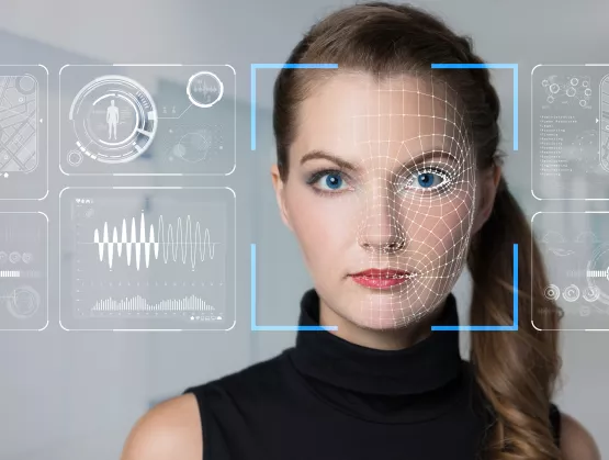
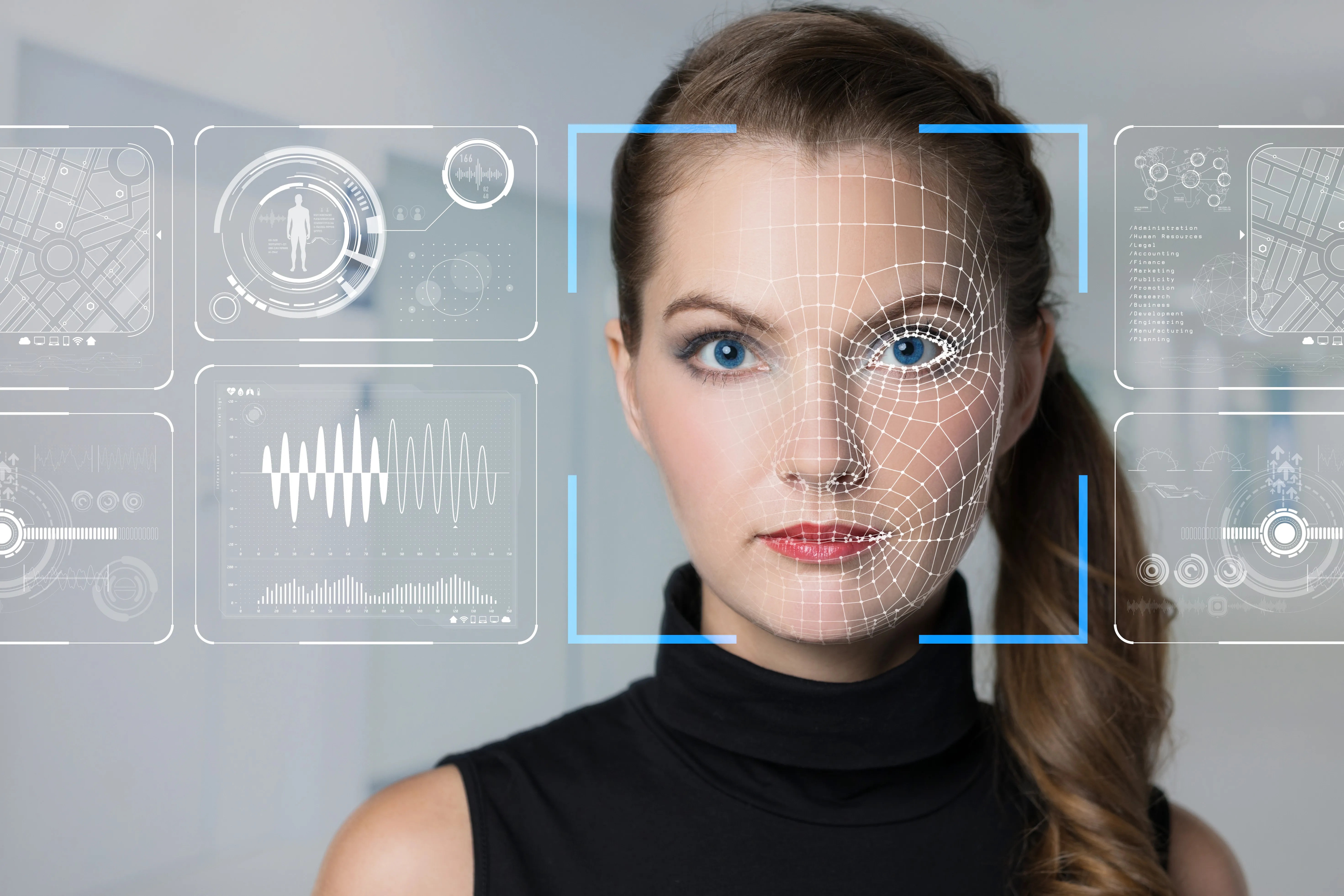
The 3D optical sensing market is once again surging – and it’s all thanks to Apple. What will we see in the next wave of end products enhanced by this technology, how will other market segments approach – and eventually use – 3D optical sensing, and which suppliers stand to gain the most from this very vital technology?Although 3D sensing, facial recognition and optical authentication systems have become only recently hot topics in the consumer electronics market, these mechanisms first made their appearance nearly a decade ago in November 2010. Following that debut, Microsoft soon launched the Kinect system in its Xbox 360 gaming console, marking a milestone as significant as Nintendo’s launch of its Nintendo Wii remote controller in 2010, which catapulted MEMS motion sensors into the high-volume consumer market.The Kinect system used a triangulation-based camera that Israeli developer PrimeSense Ltd. created and then licensed to Microsoft; Apple liked the technology so much that it acquired PrimeSense in 2013. The first version of Kinect applied the Structured Light (SL) method, a depth-sensing principle featuring an infrared (IR) laser projecting dots onto the scene, with a monochrome CMOS sensor measuring the differences in the acquired pattern. The second version of Kinect used the Time-of-Flight (ToF) principle.Kinect for Xbox360 was not only a successful consumer product; it also sparked a new market, thanks to the relatively low cost of the 3D sensing solution. By using the same hardware for Xbox 360 as in its first version of Kinect, Microsoft allowed developers to design their pet projects in the Kinect environment. Adding hand gestures controls to a PC, creating a user-controlled virtual dynamic light (see Kimchi and Chips’ demo), and developing an inexpensive hologram generator (see “Princess Leia” video from the MIT Media Lab) are just a few examples of ecosystem developers and DIYers applying their creativity to Kinect.Apple Goes 3D with Face ID3D optical sensing has expanded from gaming consoles to the smartphone. In 2017 Apple presented its Face ID camera system for the iPhone X, which they launched to celebrate the 10-year anniversary of the iPhone. Face ID is the result of a longer term strategy for Apple, the byproduct of several company acquisitions to expand know-how in 3D sensing and augmented reality (AR)/virtual reality (VR). Between 2015 and 2018, Apple acquired the camera-module maker LinX (2015), the AR startup Vrvana and the imaging sensor firm InVisage Tech (both in 2017), and AR glasses’ designer Akonia Holographics (2018).For a company that has always innovated on its own terms, Apple’s idiosyncratic approach called for deployment of the Structured Light method combined with a ToF device. The result is an amalgamation that utilizes the best features of the two mechanisms, even if the combination is one that is expensive. Apple’s addition of a near-infrared illuminator to its ToF device enhances the system’s effectiveness under most light conditions while also improving the reliability of Face ID; the overall outcome is a more satisfying user experience. The ToF component, which STMicrolectronics supplies, makes use of so-called single-photon avalanche diode (SPAD) receivers that can work with any target material and color, although a higher target illumination is required to obtain good accuracy.The other core components of the Face ID system are the Vertical Cavity Surface Emitting Laser (VCSEL, from Lumentum) and a dot projector (from ams/Heptagon), assembled together in an optical package. Apple’s expensive but reliable approach explains the company’s inclusion of the Face ID system in its latest smartphone and tablet offerings – across the iPhone Xs, Xs Pro and Xr as well as in the latest iPad Pro models. Apple’s Face ID uses facial recognition for authentication on a range of iPhone and iPad Pro models. Image courtesy of Apple. Chinese Phone Makers Get into the GameMeanwhile, other mobile handset manufacturers are rumored to be working on Face ID-like systems or have already presented similar solutions, albeit through a variety of approaches. Some have chosen to use standard ToF devices while others have adopted an SL tactic. In many of these designs, which happen to target Android systems, OEMs generally include a fingerprint sensor as a fallback biometric option to their own nascent 3D facial recognition systems. The fingerprint sensor operates in either standalone mode or integrates into the display.Chinese handset maker Oppo, for instance, uses the SL method on its Find X model with algorithms coming from Megvii. Oppo claims its equivalent of Apple Face ID is faster. I have heard that Vivo has been working on a ToF camera since mid-2018, which it claims provides greater accuracy and security in end-applications such as secure payments and unlocking the phone.Chinese technology giant Huawei’s first 3D facial sensor appeared in its Mate 20 Pro flagship mobile phone. Aside from providing facial biometrics, the front-facing 3D sensor doubles as a 3D scanner, enabling users to digitize live objects that they can then manipulate in 3D AR applications. While still a novelty, the application highlights the use of 3D light sensors beyond that of biometrics. Xiaomi’s Mi Explorer Edition smartphone features a complex SL 3D module to enable 3D facial scanning although it looks like a clone of the Apple solution.Overall, the importance of facial recognition is no longer a matter of dispute, given that Apple’s rivals are now developing counterpart offerings of their own. Leaked code from the next revision of the Android operating system (revision Q), now under development by Google, has confirmed as much. Big and Getting BiggerIHS Markit forecasts that global revenue for ToF sensors in the 3D optical sensing market will surpass $500 million in 2019, up from $370 million last year. We also predict that the ToF market will grow in the coming years, spurred by combo solutions integrated with other light sensors in the same package. This will lead to a cheaper bill of materials (BOM) compared to the BOM for the SL method.At the same time, IHS Markit forecasts that the total market potential for light sensors will be worth much more, reaching $1.5 billion by year 2022. That’s because after a solid start with gaming consoles, 3D sensing has matured and consolidated in the massive smartphone arena.A segment of 3D Sensing’s future growth will come from other use cases and applications that are emerging outside consumer electronics and mobile. These include people-counting and -tracking in consumer and industrial applications, landing-aid and obstacle-avoidance functions in drones, and car-trunk (boot) opening with foot gestures, as well as gesture recognition and passenger detection in automotive. IHS Markit predicts steady growth for ToF and other light sensors. All told, the ToF approach appears to have a greater chance than the SL method in gaining a larger market share, leading to a cheaper and smaller BOM along with reduced integration costs in system assembly and calibration.Sometime this year, Apple and other handset OEMs may include a ToF-based 3D camera on the back of the iPhone to support more immersive gaming experiences and new AR/VR applications. This will further boost the 3D sensing market.To be sure, other mature technologies are available as valid alternatives to optical 3D sensing, including ultrasonic, mmWave and radar. These alternative technologies may gain part of the total market now commanded by 3D sensing, in use cases such as obstacle-avoidance or in-cabin presence detection.To learn about 3D Optical Sensing and Light Sensors from IHS Markit, go to: https://technology.ihs.com/606483/light-sensors-for-consumer-mobile-report-2018Manuel Tagliavini, a principal research analyst at IHS Markit, covers MEMS and sensors technology.Manuel Tagliavini joined IHS Markit in 2017. His key areas of focus are MEMS and sensors for mobile and consumer technologies. He is responsible for the tracking of sensors in handsets, tablets, laptops, and sports and fitness products.Prior to IHS Markit, he spent over 10 years with STMicroelectronics, working in various roles including product engineering, program management, and marketing and business development in the company's MEMS division.Tagliavini earned an Executive Master of Business Administration at SDA Bocconi School of Management and a Master of Science in Electronic Engineering from the University of Parma, both in Italy.Stay tuned with the technological advances and market trends in the MEMS Sensors ecosystem. Join MEMS Sensors Industry Group (MSIG), the SEMI technology community that connects the MEMS and sensors supply network in established and emerging markets, allowing members to grow and prosper.
Read More
For nearly two decades, Sean Ding, CTO and chief scientist of Alibaba Cloud IoT, has worked in software and algorithm architectures, sensing, semiconductors, systems and cloud computing – all areas that have contributed to the rise of the Internet of Things (IoT). It’s no surprise, then, that Alibaba is leading next-generation innovation for the IoT. Ding will bring his expertise to his role as moderator of Brave New World - MSIG Conference on AI+IoT 2019, a half-day forum March 20, 2019, at SEMICON China in Shanghai, China. Maria Vetrano of SEMI spoke with Ding about technologies key to the IoT era including MEMS, sensors, artificial intelligence (AI), edge gateways and cloud computing. SEMI: MEMS sensors are widely used in IoT devices. What is the relationship between AI and MEMS sensors?DING: While MEMS sensors and AI will increasingly co-reside in end-user devices, I do not recommend adding AI next to the sensor (in the same package). That’s because designers continue to use the ASIC for signal conditioning, so A/D converters are still required. Rather, we should look to edge gateways to carry the majority of the workload, including deep learning, because this reduces system complexity and power consumption.SEMI: Why are smarter sensors shifting data processing and analytics to the edge of IoT devices?DING: Data processing and analytics are very important for IoT devices, but we need to focus on understanding the data, parameter calibration and more. The MEMS sensor industry should leave big data analytics to edge computing and cloud computing because AI requires deep learning, demanding a huge amount of data.The challenge is to find the sweet spot for data processing right next to the sensor element.SEMI: What is China’s evolving role in innovation in MEMS sensors for IoT devices?DING: At present, the MEMS community in China needs to figure out how to innovate instead of copying existing technologies, a low-margin business that will not help to grow the industry. One reason why I am so pleased to see the MSIG Conference on AI+IoT in China is that it will encourage greater creativity in the MEMS community in China, and this will ultimately lead to Chinese companies and R D institutions leading innovation rather than copying it.SEMI: What is the right approach to combining smart MEMS sensors with AI in IoT devices? Why is this important for both domestic Chinese and international markets?DING: Combining data from sensors with cloud-edge computing is the right approach. As sensor companies increasingly provide end-to-end solutions, such as “sensor+ firmware + SaaS + app,” we will realize easier and faster integration of sensors in IoT applications.This is incredibly important because China today is the world’s biggest market for IoT hardware. China has 2,000-plus design houses, 200-plus OEMs and thousands of distributors. That said, we still see a highly fragmented market that will benefit from a faster integration methodology.Faster integration of MEMS sensors and AI/machine learning for IoT hardware will benefit designers in international markets as well.SEMI: What do you hope MISG Conference on AI+IoT attendees will take away from the forum? DING: MEMS sensors are highly fragmented, reflecting the highly fragmented applications in which they play. The MEMS sensors industry should figure out how to provide one-stop-shopping solutions for vertical markets. This will speed the scalability of applications and expedite the growth of sensor production. Sean Ding (柯镇) will moderate Brave New World - MSIG Conference on AI+IoT 2019 at SEMICON China on Wednesday, March 20, 2019, at Kerry Hotel Pudong in Shanghai, China.This conference has been organized by the MEMS Sensors Industry Group (MSIG). Register today to connect with Sean Ding and featured speakers at the event.Speakers at the MSIG Conference on AI+IoT 2019 at SEMICON China include: Welcome and Introduction / 欢迎辞Carmelo Sansone, Director, MEMS Sensors Industry Group (MSIG), a SEMI technology community AI Needs Accurate Data – MEMS Sensors Can Provide It / MEMS传感器为人工智能提供真实数据Andrea Onetti, Group VP of Analog MEMS Group, GM of MEMS Sensor Division, STMicroelectronics Enhanced IoT Edge by Smart Sensors / 智能传感器助力IoT边缘智Bennini Fouad, Regional President Asia Pacific, Bosch Sensortec Horizon AI Processor Solution, Enable Industries in AI Time / 地平线AI芯片解决方案,赋能千万业Carl Zhang 张永谦, General Manager/VP, Smart Chip Solutions Division, Horizon Robotics Inertial Sensors in AI Applications / 运动传感器AI应用案例Ben Lee 李彬 , CEO, mCube Ultra-Low-Power Solutions: an Ecosystem Approach / 超低功耗的生态链解决方案Carlos Mazure, IEEE Fellow, Chairman Executive Director, SOI Industry Consortium High-Integrity, Fault-Tolerant Open Inertial Measurement Platform for AI-based Vehicle Automation / 适用于人工智能车辆自动控制的高集成及容错的惯性测量开放平台Dan Dempsey, Senior Director of Automotive, ACEINNA Maria Vetrano is a public relations consultant at SEMI.
Read More
At the SEMI FLEX 2019 and MEMS Sensors Technical Congress (MSTC) (MSTC) February 18-21 in Monterey, California, I had the pleasure of meeting many old friends and colleagues as well as making some great new acquaintances. With MEMS and sensors still a relatively young industry, I am delighted that our community is thriving. We continue to see double-digit growth rates, there is plenty of innovation, and the technology generates massive amounts of data that gets everyone excited about artificial intelligence, deep and machine learning, and blockchain. Those are all the buzzwords that any tech startup needs for funding these days.While it is hard to single out any one presentation at conferences, I was particularly struck by Nadia Shakoor’s keynote address, “Driving Advances in Crop Breeding and Smart Farm Management.” From Nadia I learned that the world’s largest agriculture sensing platform was a mere 45 minutes south of where I live in Phoenix, Arizona. This is a major embarrassment to admit as I have lived here for almost 30 years, have been involved in MEMS and sensors for a decade, and have a particular passion for the use of sensors in agriculture and food to improve crop yields and food quality, and to reduce food waste. This humongous sensor was hiding in plain sight right under my nose!After Nadia’s keynote, I just had to speak to her at the break. Nadia is the senior research scientist and project director for TERRA-REF at the Danforth Plant Science Center based in St. Louis, Missouri. Nadia’s work employs field-level crop phenomics, the biological study of the set of physical and biochemical traits belonging to a given organism (phenomes). Phenomes are fascinating because they change in response to genetic mutation and environmental influences. The Danforth Plant Science Center and its partners are involved in many phenotyping projects using autonomous vehicles, drones, field scanners, satellite imaging and more.After the FLEX MSTC event, I emailed Nadia to ask if I could visit the field scanner and her partner team at the University of Arizona in Maricopa, Arizona. She kindly introduced me to Maria Newcomb, a plant research scientist at the site, who gave me a good look at this mother of all field scanners: the Transportation Energy Resources from Renewable Agriculture Phenotyping Reference Platform (TERRA-REF). TERRA-REF aims to transform plant breeding by using remote sensing to quantify plant traits such as plant architecture, carbon uptake, tissue chemistry, water use and other features to predict the yield potential and stress resistance of 400+ diverse sorghum lines. The TERRA-REF Field Scanner at the University of Arizona Maricopa Agricultural Center. It’s the largest field crop analytics robot in the world, one that’s critical to the crop research underway at the Donald Danforth Plant Science Center in St. Louis, Missouri. Source: Steve Whalley TERRA-REF’s Lemnatec Field Scanalyzer is the largest field crop analytics robot in the world. This high-throughput phenotyping field-scanning robot has a 30-ton steel gantry that autonomously moves along two 200-meter steel rails that have recently been extended another 170 meters. It continuously images the crops growing below it by using a diverse array of cameras and sensors to observe the field at a dense-collection frequency with high resolution. These sensors include RGB stereo; thermal, chlorophyll fluorescence imaging system; hyperspectral cameras; a 3D laser scanner; and environmental monitors.Plant breeding is currently limited by the speed at which phenotypes can be measured, and the information that can be extracted from these measurements. Current instruments used to quantify plant traits do not scale to the thousands or tens of thousands of individual plants that need to be evaluated in a breeding program. The TERRA-REF field scanner system, on the other hand, uses sensors to scan over one acre of plants, collecting thousands of daily measurements throughout the growing season, and these are used to determine plant phenotypes and inform breeding decisions. TERRA-REF’s advanced sensor technologies include: Hyperspectral (250nm-2500nm) Thermal Infrared 2D and Stereo RGB PSII chlorophyll fluorescence 3D laser Environmental sensors The TERRA-REF field scanner platform features a massive sensor-rich scanner head. Source: Steve Whalley The humongous TERRA-REF field-scanner was certainly a sight to behold, looming like a cargo-ship container crane in the vast flat plains of the Arizona desert landscape. I’ve only scratched the surface of what this enormous sensor platform can accomplish so if you are a MEMS/sensor company interested in agriculture and food production, I encourage you to get more information at terraref.org and pay a visit next time you are in the area.Steve Whalley, CEO, Strategic World Ventures, is a strategic consultant to SEMI-MEMS Sensors Industry Group (MSIG). He also consults with established and emerging semiconductor, MEMS and sensors companies.
Read More
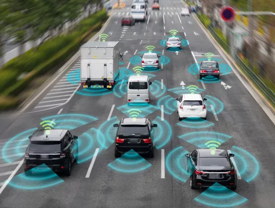
As group vice president of the Analog MEMS Group and general manager of the MEMS Sensor division at STMicroelectronics, Andrea Onetti brings nearly three decades of experience in MEMS, sensors and audio systems to his leadership role at one of the world’s most successful electronics and semiconductor manufacturers. During his keynote at FLEX and MEMS Sensors Technical Congress 2019, February 18-21 in Monterey, Calif., Onetti will address the criticality of sensor accuracy in advancing automotive, industrial and consumer applications. SEMI’s Maria Vetrano spoke with Onetti recently to give FLEX/MSTC attendees a preview of his presentation. SEMI: What are some promising advancements in sensors for autonomous cars? Onetti: The avionics industry is already successfully applying sensors for autonomous operationl. Inertial navigation systems (INS) support the operation of planes during flight, both after takeoff and before landing. Unfortunately, the technology in these navigation systems is expensive and not scalable, and they are hampered by reliability limitations in an automotive environment.Following the steady progress that we have made with MEMS inertial sensors in consumer applications, we are on the cusp of realizing greater accuracy in temperature and time – finally delivering the performance required for autonomous driving. Because we can scale in production – we’re now manufacturing more than a billion units a year – we can select the cream of this production crop for adoption in cars. Consequently, we should see Level 3 and Level 4 autonomous driving for consumers very soon.SEMI: How are companies using sensors to monitor and track their assets in industrial applications? Onetti: Predictive maintenance and asset tracking are the two main verticals in Smart Industry. The adoption of multiple sensors for condition monitoring is helping to detect the faulty operation of equipment and to detect early signs of issues that are otherwise difficult to capture. Ultrasonic microphones can detect leaks in a pipe at an early stage, accelerometers with high bandwidth can act as micrometers, and accurate temperature sensors can catch overheating. Similarly, in asset tracking, we use temperature monitoring in combination with inertial sensors to detect problems during the transport of goods. Shock sensors with extremely high full scale (up to 8000g) can tell whether a lightweight envelop has been dropped. Pressure sensors can switch off a radio system when a cargo plane takes off and can mute smart trackers in compliance with flight regulations. We really can do almost anything! A full slate of ST sensors and microcontroller units (MCUs) enable WEG’s small but powerful motor sensor, which listens to a motor, feels its pain, and shares that information with engineers, operators and others to diagnose problems before they happen. Image courtesy of STMicroelectronics. High-accuracy motion, environmental and proximity sensors are crucial to VR/AR. Image courtesy of STMicroelectronics. SEMI: How will sensors advance user experiences in consumer electronics, such as VR/AR systems?Onetti: Virtual reality (VR) and augmented reality (AR) are great examples of promising consumer technologies that will become pervasive as performance of inertial sensors improves. First, we need super accuracy in time and temperature to provide the right experience to users. To achieve this level of accuracy, we need a major step forward in performance, and that includes power consumption and miniaturization. Fortunately, we are constantly making progress in the high-accuracy motion, environmental and proximity sensors that are critical to these systems. While the scale is vastly different between VR/AR and automotive, the requirements for AR/VR systems are pretty similar to those that will enable autonomous cars. A growing variety of sensors (environmental, microphone, proximity, motion) – combined with a sensor hub in an MCU – are central to VR controllers (above) and VR head mounted displays (below). Images courtesy of STMicroelectronics. SEMI: We don’t hear much about the criticality of higher accuracy in sensors. Why is improving accuracy in sensors especially important – and what role do calibration routines play in achieving higher accuracy?Onetti: A sensor is more than just the performance of the relevant function. It is also the intrinsic accuracy that it brings. This accuracy is tuned by calibration, which is typically an expensive process done at the end of product manufacturing or – better still – during earlier stages of manufacturing.Today more applications require sensors with higher accuracy, which necessitates investing more time in calibration, leading to higher cost.MEMS technology can help by offering solutions with intrinsic higher accuracy, which reduces the cost of calibration for product manufacturers. This naturally delivers major benefits to OEMs and, ultimately, their customers.SEMI: What would you like FLEX and MSTC attendees to take away from your presentation?Onetti: As attendees explore the wide variety of available sensor solutions for their end products, I would ask them to prioritize the role of accuracy in sensor selection – because improved accuracy means higher quality data, and higher quality data means better decisions with reduced need for data processing.While designers understand the role of calibration routines in qualifying individual components for specific applications, it is the continuous evolution of MEMS technology that offers the best possibility of breakthrough reductions in time and cost of these calibration routines. This makes MEMS sensors more attractive and affordable than similar sensor components based on different technologies. Andrea Onetti will present Accuracy Enables MEMS Sensor Pervasion at FLEX/MSTC on Tuesday, February 19 at 11:00 am.Register today to connect with him at the event. To learn more about STMicroelectronics, click here. Maria Vetrano is a public relations consultant at SEMI.MSTC FLEX 2019 is organized by MEMS Sensors Industry Group (MSIG) and FlexTech.Maria Vetrano is a public relations consultant at SEMI.
Read More
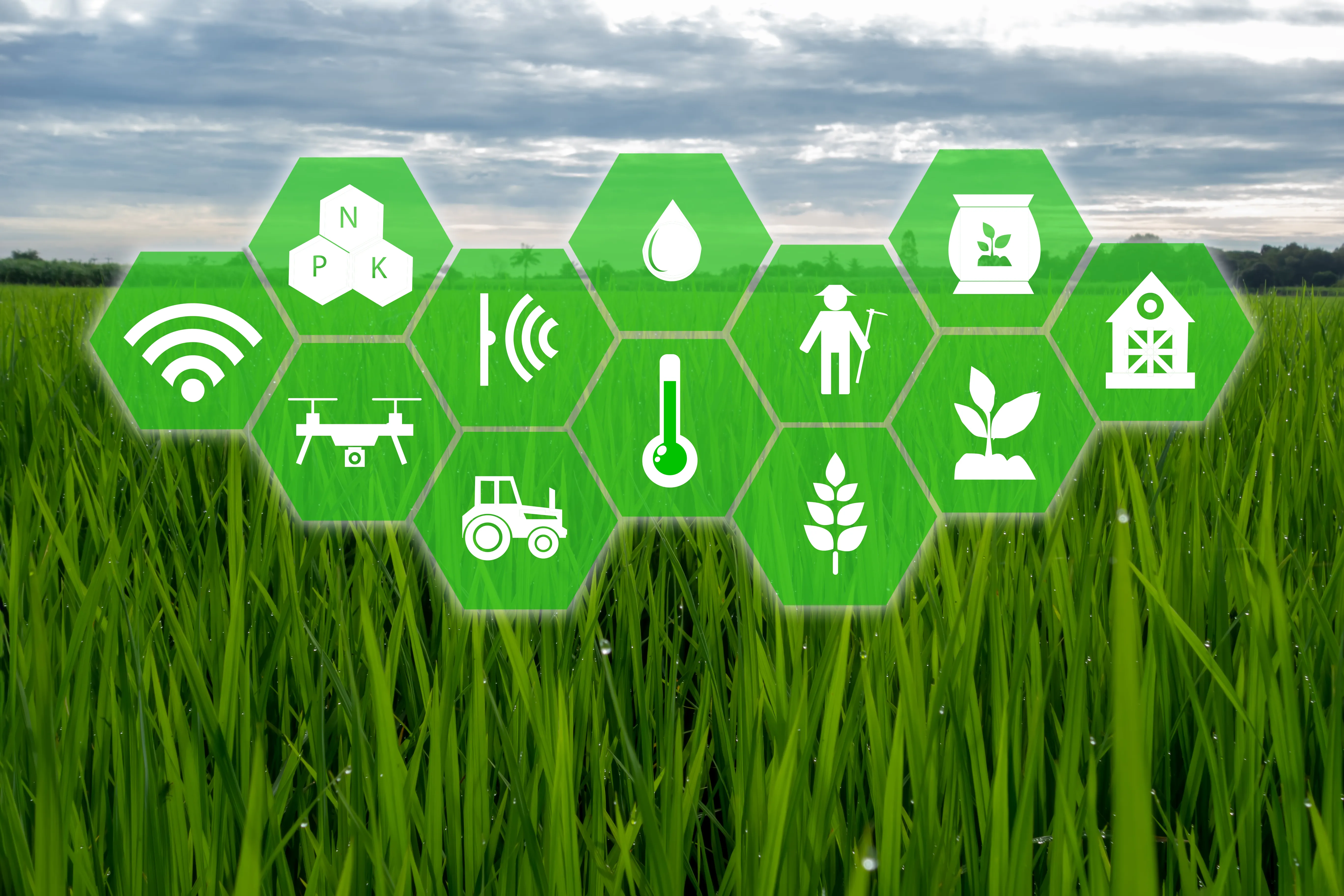
Jason Jelinek, a software technical manager at John Deere Electronics Solutions, has parlayed his more than two decades of embedded software engineering experience into commercializing controls and sensing technologies for rugged/harsh environments, including agriculture/off-road and aerospace. During his keynote at the upcoming FLEX and MEMS Sensors Technical Congress 2019, February 18-21 in Monterey, Calif., Jelinek will address the driving need for advanced sensing technologies that will fuel the continued growth of autonomy in agriculture.SEMI’s Maria Vetrano asked Jelinek to help FLEX/MSTC attendees understand his vision of autonomy in agriculture, which heavily leverages advanced sensing technologies to help farmers master equipment logistics, handle vehicle- and fleet-level operational efficiency, and manage the entire lifecycle of crops.SEMI: Did autonomy in agriculture start with autonomous equipment, such as tractors and combines?JELINEK: Automation, the first step on the road to autonomy, has been occurring in agriculture for a long time. Over the past 100 years, automation has dramatically reduced manual effort and simplified jobs in farming, allowing operators to focus more on administrative and other aspects of their work.The evolution of the combine is a good example of automation in agriculture. Long ago farmers would use a scythe to cut down the crop before bundling or stacking it up. Later they would manually thresh and winnow the crop to get the grain. Over time, we developed windrowers to cut the grain, threshing machines to separate the grain from the chaff, and winnowing machines to get only the grain. Combines now “combine” all those steps to go from grain on the stalk in the field to grain in the hopper. One person in a combine can do the work that once required many people and animals — all in a much shorter timeframe. We are now looking at automating harvesting to maximize yield and reduce fuel consumption. The AUTOTRAC feature on John Deere machines is a recent example. AUTOTRAC divides a field into rows based upon the parameters of the machine in operation, supporting hands-free driving with very high accuracy. It allows consistent, accurate rows for tilling, planting, crop treatment and harvesting, saving considerable time, improving overall quality and freeing the operator to do other work while in the vehicle.The Exact Emerge and Section Control features (which also use AUTOTRAC) will spur greater future autonomy. Control over both the seed spacing (Exact Emerge) and when the machine drops seeds (Section Control) prevents overseeding and provides the right seed-spacing for optimal crop production.As we look to the future, sustained growth in automation of jobs will enable the development of fully autonomous equipment. Currently, however, skilled operators are still closely involved in job management and execution. To realize greater autonomy, we will need machines that make the decisions once made by people.SEMI: How will autonomy in agriculture change the ways that we grow and harvest food — and even affect when we sell it?JELINEK: Autonomy will lead to more efficient production, reducing fuel, fertilizer, herbicide and water requirements. It will also enable fewer people to do more of the work.Let’s start with conditions that are hard, even impossible, to control: weather and staffing.While farming is still tied to the weather — and will remain so for some time — more efficient operations will allow tilling, planting, spraying and harvesting of fields to occur in shorter time windows that more easily match conducive weather conditions.There is also a human-resource issue: The agricultural industry must compensate for population decline in the rural areas where farmers operate. Doing more with less is essential for agriculture to continue to meet the rising food and clothing demands of the world’s population.SEMI: To what degree will we see artificial intelligence in autonomous agricultural systems?JELINEK: While autonomous systems had their start at the vehicle level, they will one day move to the entire fleet, providing suggestions on when the owner should execute operations. Autonomous systems may also help owners to decide when to store or sell crops, based on market conditions, operating costs and desired margin levels. That’s the initial level of artificial intelligence that I foresee.SEMI: How can sensing improve autonomy in agriculture?JELINEK: The challenges we face in agriculture are many, but technology will help us meet them. We must transfer responsibility for operations and decision-making from the skilled operator to the intelligent machine. Through increased use of sensing, we can gather large amounts of data, which autonomous agricultural systems will process, communicate and interpret to streamline jobs and boost agricultural production.SEMI: What would you like FLEX/MSTC attendees to take away from your presentation?JELINEK: I would like FLEX/MSTC attendees to understand the environment in which agricultural sensors need to operate. We need sensing solutions that will survive and thrive in rugged, outdoor variable environments to support the automation that will fuel autonomy.I would also like to engage suppliers in the application of current technology to meet our sensing needs.Jason Jelinek will present Autonomy in Agriculture at FLEX/MSTC on Tuesday, February 19 at 9:00 am.Register today to connect with him at the event. To learn more, click here.MSTC Flex 2019 is organized by the MEMS Sensors Industry Group (MSIG) and FlexTech. Maria Vetrano is a public relations consultant at SEMI.
Read More
4 Key Takeaways from SEMI Taiwan Member ForumThe rapid development of artificial intelligence (AI) has accelerated the digital transformation in various industries and has now fused with Internet of Things (IoT) to exploit the value of both technologies in reshaping the electronics industry value chain. As it emerges from the shadows of its parent technologies, AIoT is giving rise to new opportunities in manufacturing, healthcare, transportation, and even energy. AIoT is fast rising in prominence as an enabler of key electronics manufacturing process improvements and the creation of add-on value to existing products – both critical to the success of many businesses.SEMI and the SEMI MEMS Sensors Industry Group (SEMI-MSIG) held a technical forum on smart sensing and its applications in AI and AIoT, inviting renowned experts in sensors and edge computing to share in-depth insights into the latest AIoT technologies and applications with more than 100 industry professionals in research and development, marketing and sales. Here are four key takeaways from the SEMI Taiwan member forum.1. Steady Growth for Global Sensors MarketThe global sensors market’s steady growth is expected to expand at a CAGR of 6.6 percent from 2017 to 2023, with Asia driving the biggest gains and automotive leading the segments – including healthcare and education – with the strongest growth. Automotive alone is expected to reach US$34 billion in 2023.2. Integration Critical to MEMS Sensors DesignsWith AI booming, MEMS sensor designs need to drive toward greater integration —not only integrating data collection with sensors, but also streamlining data processing on the backend – making 3D models of today’s MEMS mechanical designs critical. The differences between 3D and entrenched 2D models are dramatic, elevating the importance of specifying manufacturing steps in MEMS designs. As new sensors and applications continue to emerge, companies that develop the most powerful integrated designs will win. 3. Growth of Smart Voice-Control Applications to ExplodeAIoT is also accelerating the development of smart voice-control applications and the rise of new related business opportunities. Just 50 million voice-controlled devices shipped worldwide in 2017, a number predicted to swell to 436 million in 2021 with smart home devices such as set-top boxes and smart TVs the major growth drivers.4. AIoT Eyed to Make Human-Robot Collaboration SafeSafety is an essential feature for human-robot collaboration. Tactile sensing technologies give robots a layer of “skin” with capabilities rivaling human touch. To ensure humans and robots work together safely in work environments, sensors on this layer of skin are concentrated – less than 8mm apart, equivalent to the width of a human finger, with a response time of less than 5ms on contact. More than 4 million robots worldwide are expected to be upgraded with these sensing technologies and are on track for deployment in pilot plants in the next three years.SEMI-MSIG is committed to strengthening connections across all sectors in the MEMS and sensors supply chain, working closely with the industry to accelerate the development of related technologies and applications in both mature and emerging markets. In addition, SEMI-MSIG hosts regular events to inspire business opportunities and technology exchange for innovative applications, while enhancing the visibility of members among global customers and partners to help them forge new partnerships. To join the group, contact SEMI Taiwan’s Helen Chen at [email protected] Yi is a marketing specialist at SEMI Taiwan.
Read More