downloadGroupGroupnoun_press release_995423_000000 copyGroupnoun_Feed_96767_000000Group 19noun_pictures_1817522_000000Member company iconResource item iconStore item iconGroup 19Group 19noun_Photo_2085192_000000 Copynoun_presentation_2096081_000000Group 19Group Copy 7noun_webinar_692730_000000Path
Skip to main content
Default Banner Image

sensors

The BioMEMS market is becoming increasingly diverse, encompassing gas and pressure sensors, ultrasound, specialized biomedical sensors, and other types of MEMS and microfluidic chips used for drug delivery and analytical applications. The BioMEMS market is also growing steadily: Research firm Yole Développement predicts that BioMEMS will grow at 14.9% CAGR from 2017-2023, reaching US$6.9B by 2023.1 As a high-value market, BioMEMS is worth pursuing as long as you can manage the complexities of manufacturing, including a sometimes-fragmented supply chain. Fortunately, the MEMS manufacturing ecosystem is evolving to accommodate the needs of companies that are in the process of commercializing BioMEMS-enabled products. Understanding the ecosystem’s shifting dynamics will help BioMEMS to flourish in this promising while often-challenging market segment.Unique Product, Unique ProcessIn the world of semiconductor manufacturing, it is routine for a fab to manufacture hundreds of different device designs using just a handful of process nodes. Semiconductor foundries share their design rules with customers, who then develop the mask set accordingly, literally adapting their designs to fit the rules for manufacturing on one of the foundries’ process nodes. In stark contrast, most MEMS devices cannot conform to the level of standardized manufacturing processes that work so well for semiconductors. Rather, MEMS challenges us to develop individualized processes for each device. It’s one product, one process.New BioMEMS designs generally emerge from either corporate R D or academia, two groups that approach specialized MEMS foundries such as ours when they’re entering pilot or low-volume production. Today successful commercialization depends on open, accurate communication and close collaboration. MEMS foundries must work side-by-side with designers to ensure that designs are based on real-world manufacturing process technologies. This highly customized manufacturing model makes it very difficult to support future demand for the groundswell of diverse BioMEMS devices that are in development. If we want to handle this upward trajectory of BioMEMS, we’ll need to adapt.Change the ModelWhile most existing MEMS foundries currently support a wide variety of devices types, I predict that market forces will cause our foundries to move toward specialization. Some companies will specialize in what they already do best, e.g., inertial sensors for the automotive industry. Others might choose to develop their foundry business around a purpose-built facility, which, for example, only manufactures microfluidics or magnetic devices. Larger enterprises might opt to build captive foundries that are designed to serve their specific needs. Get Creative: Combine, CollaborateSatisfying the thriving market for BioMEMS will require creativity. One idea: combine different disciplines of the manufacturing process at the same foundry. For example, we could have a biochemistry fab and a MEMS fab under the same roof, or we could have a MEMS fab and a packaging facility in one building. While these approaches may not yet exist outside of academia, necessity may drive them to fruition.It will also require heightened strategic collaboration, a process that has already begun. To support both large volumes and greater diversity of devices, some MEMS foundries are building cooperative relationships with former competitors. Think of it as a restructuring of the supply chain.Embracing the special challenges of BioMEMS manufacturing is worth our investment in time and resources. We need to step back, individually and collectively, to understand where each of the existing MEMS foundries fits into the new supply chain so we can leverage our strengths. We can start by forging stronger alliances for tech transfer. Once we more freely share information as we engage in joint product development — involving technology teams who are more connected and less guarded — we will expedite tech transfer and manufacturability.While we are unlikely to achieve the same level of standardization that has enabled the semiconductor industry to reach its great heights, as long as we evolve to meet demand, we will grow together and prosper.To learn more about this topic, meet with Jessica Gomez at the upcoming SEMI-MSIG MEMS Sensors Executive Congress (October 22-24, 2019 in Coronado, Calif.) or email her: [email protected][1] “BioMEMS Emerging Non-Invasive Biosensors: Microsystems for Life Sciences Healthcare 2018 Report,” Yole Développement, https://yole-i-micronews-com.osu.eu-west-2.outscale.com/uploads/2018/08/Sample-BioMEMS-Non-Invasive-Sensors-Microsystems-for-Life-Sciences-Healthcare-2018-.pdf As founder and CEO of Rogue Valley Microdevices, Jessica Gomez has created a world-class precision MEMS foundry and wafer fab in the heart of Southern Oregon. Integral to her role as CEO, Ms. Gomez practices a business philosophy of offering custom design, best-in-class process technology and R D expertise to customers, to help them achieve the highest quality and reliability in their products.In 2018, Ms. Gomez was selected for the prestigious SEMI Board of Industry Leaders. SEMI also recognized her in its first Spotlight on SEMI Women, which honors accomplished women in the global microelectronics industry.Prior to founding Rogue Valley Microdevices in 2003, Ms. Gomez honed her experience in semiconductor processing and production management through positions at Standard Microsystems Corporation, Integrated Micromachines and Xponent Photonics.For more information, visit: https://roguevalleymicrodevices.com/Rogue Valley Microdevices is a longtime member and supporter of SEMI-MEMS Sensors Industry Group, which connects the MEMS and sensors supply network, allowing members to address common industry challenges and explore new markets.
Read More
Automotive original equipment manufacturers (OEMs) and their direct suppliers of parts and systems share a vision: Next-generation vehicles will be more electric, autonomous and connected. At a market size of more than $1 trillion, automotive is steadily becoming a high-tech market as cars morph into advanced technology platforms with partially or fully autonomous features. Call them semiconductors on wheels. Big players such as Google and many carmakers are investing heavily in chip advances to help drive increases in silicon content in automobiles.At SEMICON Europa, Pierrick Boulay, Solid State Lighting and Lighting Systems analyst at Yole Développement, will provide a market update on autonomous automobile trends including the state of sensors, radars, cameras and LiDARs as the industry works to increase the level of autonomy and electrification.Autonomous vehicle design can only thrive with the development of an industry standard for chip and device traceability across the supply chain. The importance of chip traceability to the automotive industry is reflected in its central role in driving a chip traceability standard.According to Heidi Hoffman, senior director of technology communities marketing at SEMI, “chip traceability is one of the next big things for the technology industry. The benefits are enormous, and the upsides – including yield enhancements, counterfeiting safeguards, and support for new applications – are plentiful. But the implementation challenges of chip traceability are also big and will require considerable effort to overcome. The biggest hurdle of all? We need to transcend industry fears by demonstrating that we can secure IP when it is shared across the hardware supply chain.” The Importance of Standards, Data Collection and Collaboration Across the Supply ChainThe automotive industry has long embraced tracing the sources of defects. Now, as the automotive and semiconductor supply chains increasingly overlap, traceability has taken on greater importance in the semiconductor industry. SEMI committees, task forces and events such as the Smart Transportation Forum at SEMICON Europa are ideal platforms for collaborating to develop new standards and best practices for the automotive industry.Earlier this year, German luxury automobile maker Audi AG became the first automotive original equipment manufacturer (OEM) to join SEMI as member, strengthening alignment across automotive supply-chain segments. At SEMICON Europa, the SMART Transportation Forum and Pavilion, staged by the SEMI Global Automotive Advisory Council (GAAC) and bolstered by the Electronic System Design Alliance, a SEMI Strategic Association Partner, will gather key stakeholders across the automotive value chain, from design and semiconductor equipment to materials and carmakers, to explore innovation opportunities in automotive electronics. SEMI Global Automotive Advisory Council (GAAC) “If the industry wants to reach the goal of zero defects, a new collaborative approach is necessary,” observed Antoine Amade, senior regional director EMEA at Entegris. At SEMICON Europa, Amade will present new ways to collaborate in reducing chip defectivity and meet other challenges in the automotive industry.More than half of semiconductor failures on the automotive assembly line today (so-called 0km failures) are traced to semiconductor fab defectivity. “The increasing semiconductor content in automobiles – driven by growth in ADAS, electrification and autonomy – has put a growing focus on the quality and reliability of these devices and their implications for consumer safety and satisfaction,” said Oreste Donzella, senior vice president and CMO at KLA.The smart manufacturing (Industry 4.0) revolution is already spurring higher performance and great efficiencies throughout the supply chain and will also be crucial to driving innovation in automotive. Smart manufacturing makes possible significant improvements in factory key performance indicators (KPI) for cycle time, on-time delivery, overall equipment effectiveness, cost and product quality.“These KPI gains are key to meeting quality levels the automotive industry must reach to support the deployment of autonomous driving vehicles,” said John R. Behnke, general manager of Final Phase Systems at INFICON. In his talk at SEMICON Europa, Behnke will provide an overview of existing, in-progress, and future smart manufacturing solutions for the semiconductor industry and their impact on the automotive supply chain. The SMART Transportation Forum, 13 November, 2019 (9:30-15:30 at ICM Munich, room 14c) at SEMICON Europa is the premier platform for key stakeholders to connect, collaborate and innovate across the automotive value chain. Automotive and semiconductor industry experts will offer insights into trends in design, semiconductor equipment and materials, and automotive innovation and the roadmap to 2030. The SMART Transportation Forum will also showcase innovations in imaging, sensing, artificial intelligence (AI), smart manufacturing and L5 mobility.Other SEMICON Europa highlights: Advanced Packaging Conference: Packaging and Test Challenges Towards High Reliability (12-13 November 2019) 23rd Fab Management Forum: Game Changers for Semiconductor Operations(11-12 November 2019) Strategic Materials Conference: Strategic Materials Enabling Industry Roadmaps(12-13 November 2019) SEMICON Europa registration is open for visitors and exhibitors. For more details, please visit the SEMICON Europa website and connect with SEMI Europe on Twitter or LinkedIn @SEMIEurope (use #SEMICONEuropa).Learn more about the SEMI chip traceability standard – SEMI T23 - Specification for Single Device Traceability for the Supply Chain – and SEMI Technology Communities.Serena Brischetto is a marketing and communications manager at SEMI Europe.
Read More
Stefano Zanella, Head of Automotive, Industrial and Location Businesses, TDK InvenSense will present at next month’s SEMICON Taiwan (September 18-20, 2019 in Taipei City, Taiwan). SEMI Taiwan’s Emmy Yi spoke with Stefano for a preview of his talk.SEMI: What macro market trends are driving automotive manufacturers to increase the variety and volume of MEMS sensors in cars?Zanella: The car world is changing. Consumers increasingly view car ownership as less desirable, yet the number of miles traveled and of hours spent in a car are rising steadily. At the same time, cars are changing profoundly, and the pace of change is rapid. To thrive in this new world, automakers are becoming transportation enablers and providers.Many vehicles today autonomously interact with humans and the world around them, operate with less or no human control, and are powered by electric batteries. MEMS sensors – which mimic and augment the five human senses – are front and center in these advancements.Unlike other types of sensors – such as cameras, radar and GNSS/GPSS – MEMS gyroscopes are functional in every environment. Gyroscopes, as well as accelerometers, can supplement those other sensors when they are not available and boost the accuracy of their outputs when they are available. Both camera stabilization and dead reckoning when GNSS is unavailable are good examples of the latter. Other prevalent sensors include MEMS microphones, used to capture voice commands, ultrasonic sensors, which can be leveraged for parking and gesture recognition, and fingerprint sensors, which can improve car security.SEMI: How can automakers stay competitive in this changing landscape?Zanella: Automakers can future-proof their relevance in the transportation market in several ways. By embracing consumer migration toward ride-sharing over car ownership, many are transforming from manufacturers to mobility providers. Carmakers that invest in ride-sharing and other modes of transportation (e.g., scooters) can sustain their profitability, even if the number of vehicles sold eventually shrinks or simply doesn’t grow as much as anticipated.Automakers will need to pursue new avenues of product differentiation. Traditionally, automakers have kept performance and aesthetics to themselves by owning the engine and the body design of the car, leaving nearly everything else to suppliers. Autonomous driving and electrification, however, are pushing automakers to own the battery pack and the autonomous driving software stack.While we are just beginning to see standardization in battery packs, automakers are likely to own the autonomous driving stack for many years to come. Automakers that offer cars with highly functional and efficient batteries and driving stacks stand to gain market share.Automotive infotainment systems will become increasingly crucial as autonomous driving turns everyone into a passenger. Audio subsystem providers such as Harman Kardon, Bose, and Bang Olufsen, for example, jockeyed for attention at the most recent Geneva Motor Show, demonstrating sophisticated surround-sound systems that rival premium-quality home audio setups.With more and more consumers using voice interfaces to interact with devices in the home, drivers are less willing to accept spotty accuracy in the car. Hence, automakers are using more higher-performing MEMS microphones to accurately capture voice commands. This will come as a relief to those of us who routinely yell at our steering wheels while using voice command to try to call home. Demand for higher quality infotainment systems has prompted some automotive OEMs to own the entire infotainment system and work directly with sensor and chipmakers, a level of intimacy that gives automakers a chance to tune sensor and chip development to their own needs. This tighter relationship also positions device suppliers to forge more direct links with drivers.SEMI: Which MEMS sensors are particularly important to tomorrow’s automobiles and why?Zanella: For many years the automotive industry has been integrating more electronics into cars to improve safety, advance the driver and passenger experience, and, more recently, power the car. As vehicles rely less on human control, automakers must replace the senses of the driver with something else. That something else is a bunch of sensors, microphones, cameras, radar and LIDAR to replace vision and hearing.Since MEMS sensors such as accelerometers, gyroscopes and pressure sensors are much more robust than other types of sensors to operate in snow, rain and darkness and other imperfect environments, automakers use them to ensure that the vehicle never gets lost when other sensors and/or the GPS/GNSS signal become unavailable in tunnels or urban canyons. Gyros help determine direction, accelerometers velocity and distance driven, and pressure sensors height, such as when taking a fork on a multi-level highway. At the same time, fingerprint sensors, ultrasonic parking sensors, and temperature sensors are improving convenience, safety and security for the car’s occupants. Automakers increasingly use inertial and environmental sensors, MEMS microphones, fingerprint sensors, and vision/imaging sensors to augment or replace the five human senses on which car drivers have relied for over 100 years. Source: TDK InvenSense SEMI: To what degree can MEMS sensors enable automotive security?Zanella: MEMS sensors are used widely to enhance security today. Some of their mechanisms are easy to understand while some are unexpected. For instance, ultrasonic fingerprint sensors can authenticate the driver of a vehicle to prevent car theft or something less onerous, like a teenage driver taking the car out without permission.Accelerometers and gyroscopes can prevent a new type of spoof on keyless entry systems. Imagine that you are very close to your vehicle. Your car senses the remote control in your pocket and automatically opens the doors when you pull the handle. Now suppose that your car is parked on the street, not far from your house. You leave the remote control home, and the car doesn’t sense the proximity of the remote control. Great! No one can enter your car, unless ... a thief has a big signal amplifier that makes your car think that the keyless entry device is next to the car. In this case, what can an automaker do? Add an accelerometer that restricts the keyless device from broadcasting the entry signal unless you are walking to the car with the device on your person.SEMI: What would you like SEMICON Taiwan attendees to take away from your presentation?Zanella: I would like them to embrace the transformations afoot in the automotive market as well as their associated design challenges since, by overcoming these hurdles, they can offer significant societal benefits such as safer and cleaner transportation. At the same time, these transformations mean significant opportunities for semiconductor industry revenue growth. And while design-to-delivery cycles in automotive are longer than in consumer and mobile, the automotive market supports higher-value devices as well as the chance to fold dozens of MEMS sensors into a single model.To paraphrase Lord Kelvin: If you can’t sense it, you can’t manage it. As suppliers of many key technologies that make intelligent transportation possible, the MEMS sensors industry is in an excellent position to help automakers manage the many challenges ahead.Stefano Zanella, Ph.D., is Head of Automotive, Industrial and Location Businesses at TDK InvenSense, where he brings MEMS sensors (including accelerometers, gyroscopes and microphones) and location solutions to the automotive and industrial markets. Zanella holds an MS and a Ph.D. in Electrical Engineering from the University of Padova, Padova, Italy as well as MBAs from both the UC Berkeley Haas School of Business and from Columbia University.He will present MEMS Sensors Enabling the Smart Car Revolution on Wednesday, September 18, 2019, at SEMICON Taiwan at 1F 4F, Taipei Nangang Exhibition Center, Taipei City, Taiwan. Register today and save 20% to learn how MEMS sensors are transforming the human experience with cars.Connect with Stefano Zanella at SEMICON Taiwan or via LinkedIn. You can also get more information on TDK’s automotive solutions and application guides online.Interested in engaging with the MEMS sensors supply chain? SEMI MEMS Sensors Industry Group is a technology community that enables professionals in the MEMS and sensors industry to innovate, address common challenges and accelerate business results.Emmy Yi is a marketing specialist at SEMI Taiwan.
Read More
Despite market saturation and stagnation saddling many business sectors, MEMS remains a shining star in the semiconductor industry. Opportunities in automotive, consumer electronics, mobile, medical are rising. What is supporting this industry growth? Who are the big players on the horizon?SEMI spoke with Dimitrios Damianos, Technology Market Analyst, Photonics, Sensing and Display division at Yole Développement, about MEMS market dynamics and future trends. Damianos shared his views ahead of his presentation at SEMI MEMS Imaging Sensors Summit, 25-27 September, 2019, at the WTC in Grenoble, France. Join us at the event to meet experts from Yole and many other key industry influencers. Registration is open.SEMI: MEMS and sensors is one of the healthiest industries not only in Europe but globally. Despite a global economic slowdown, the MEMS and sensors is still growing. What is fueling this growth?Damianos: The value of the global MEMS and sensor market will almost double from $48 billion in 2018 to $93 billion in 2024. In 2018 the MEMS and sensor market represented more than 10% of the total IC market, as more and more MEMS devices and sensors, such as MEMS, image sensors, and RF filters, are integrated in end products in consumer and automotive. In particular, the value of the MEMS-only market reached $11.6 billion in 2018, with consumer applications accounting for more than 60% of the total market. From 2019 to 2024 the MEMS market will grow 8.3% annually in value driven by pressure (for TPMS), RF (for V2X 5G communications), inertial (for ADAS) and future MEMS (such as pMUT for ultrasonic fingerprint) (Source: Status of the MEMS Industry report, Yole Développement, 2019). SEMI: How are MEMS shaping the semiconductor industry today? Damianos: MEMS have a make-smarter enabling capability. They are providing context for new applications and services in transportation, mobility, health, and security. Large companies such as Alibaba and Google are considering MEMS as a critical element in their business solution domains covering the upcoming smart home, smart campus, smart city and smart industry applications. MEMS have key features that correspond to these companies’ criteria for accuracy, small size (without performance degradation), low power and always on (e.g. microphones). Furthermore, with the advent of sensor fusion and edge computing, more sensor data can be processed, maximizing the qualitative and useful information about us and our surroundings. This has a huge impact in all markets, especially consumer.SEMI: MEMS foundries performed well thanks to the boom in industrial and medical applications. Who are the big players right now?Damianos: During 2018, all foundries saw their revenue increase. STMicroelectronics, Teledyne Dalsa, Silex, IMT, Micralyne and Philips Innovation Service are important MEMS foundry players that offer services for various MEMS devices used in medical and industrial markets, among others. On one hand, medical applications were driven mostly by microfluidics, flowmeters, pressure and inertial MEMS. On the other hand, industrial applications were driven by inkjet heads, microbolometers and pressure MEMS. The market prospect, however, is huge for RF MEMS and oscillators that will be used in next-generation 5G infrastructure. SEMI: What is the current status of MEMS for automotive applications? What are the related market drivers? Damianos: In automotive applications, accelerometers and pressure sensors still account for the lion’s share in units. Pressure sensors will grow at more than 8% with Tire Pressure Monitoring System (TPMS) implemented in Chinese vehicles in the near future. After 2019 and 2020, with the new Chinese standard, GB 2614, TPMS will become compulsory: 100% of all new vehicles will have TPMS. Also, automotive MEMS could grow quicker than the corresponding car market (currently at approximately 3%). The reason is a higher number of many different MEMS devices that are being integrated in cars, such as MEMS inertial measurement units (IMUs), TPMS, environmental MEMS for gas and particle monitoring in-cabin and microphones for hands-free voice commands.SEMI: After years of decline, the inkjet heads industry is growing again. What other segments are benefiting from MEMS technology applications? Can you name two examples?Damianos: RF MEMS (BAW filters) is also benefiting from applications in smartphones and will continue to benefit with the arrival of 5G. 5G means additional high frequency sub-6 GHz bands that can only be addressed by BAW filters. Moreover, new infrastructure approach using active antennas will create an expanding market for BAW.Another segment is inertial sensors. Inertial MEMS already have a high potential in wellness and fitness wearables and are gaining support for medical wearable applications to monitor patient activity, with the aim to prevent seizure in cases of epilepsy and other mental disorders. Compared to other types of sensors, MEMS is the golden technology for inertial sensors integrated into medical wearables. They are used for rehabilitation systems, activity trackers and assistance living/fall detection. Specifically, the IMU market will continue to grow for consumer and automotive applications as their price and form factor continue to shrink and they replace traditional standalone MEMS accelerometers and gyroscopes. However, the inertial sensor market will mostly grow for smartphone applications (mostly 6DOF, with 9DOF volumes being comparatively low).SEMI: Give us one prediction about the opportunities offered by the MEMS technology. Damianos: Sensor fusion is becoming more and more relevant since billions of MEMS sensors are made every year. The upcoming 5G revolution will make connectivity easier than ever, creating exponentially more data. To make these data meaningful, data processing is mandatory. Big data is an industry born of recent advancements in AI and machine learning, built upon and fueled by a wealth of new data from ever-expanding sensor applications. An upcoming trend is edge computing, with sensors and MEMS driving a new age of technology. Sensors are digitizing the human experience, and as the real and virtual worlds move closer together, it will be sensors that bind them, enabling new experiences for users everywhere. Running AI at the edge, coupled with sensor fusion, will open new applications for MEMS in audio, motion, olfactometry, and imaging. We also expect that new MEMS devices (microspeakers, ultrasonic fingerprint, pMUT) and piezoelectric MEMS technology could rejuvenate the MEMS market. SEMI: What are your expectations for SEMI MEMS Imaging Sensors Summit and why would you invite your peers to attend? Damianos: SEMI is organizing another very successful event, gathering experts from the Imaging and MEMS industries. We are at a turning point of innovation, with many technological advancements in AI, IoT, AR/VR, biometrics, and other areas where Imaging and MEMS technologies are paramount. Yole is excited to hear the thoughts of many high-profile experts on existing activities and future prospects within their organizations. If you are too, then it is an event that you shouldn’t miss!Dimitrios Damianos, Ph.D. is a Technology and Market Analyst in the Photonics, Sensing and Display division at Yole Développement (Yole). Damianos is a member of a Yole team that produces technology and market reports on the imaging industry including photonics and sensors. Damianos holds a MSc degree in Photonics from the University of Patras (Greece). After his research on theoretical and experimental quantum optics and laser light generation, Dimitrios pursued a Ph.D. in optical and electrical characterization of dielectric materials on silicon with applications in photovoltaics and image sensors, as well as SOI for microelectronics at Grenoble’s university (France). He has also authored and co-authored several scientific papers in international peer-reviewed journals. Learn more! Join the webinar on 5th September 2019. Registration is open! Serena Brischetto is a marketing and communications manager at SEMI Europe.
Read More
In the long unfolding arc of technology innovation, artificial intelligence (AI) looms immense. In its quest to mimic human behavior, the technology touches energy, agriculture, manufacturing, logistics, healthcare, construction, transportation and nearly every other imaginable industry – a defining role that promises to fast track the fourth Industrial Revolution. And if the industry oracles have it right, AI growth will be nothing shy of explosive.“The gains these days are not incremental,” said Ajit Manocha, SEMI president and CEO, said to a gathering in July of the Chinese American Semiconductor Professional Association (CASPA) for its Summer Symposium at SEMI’s headquarters in Milpitas. “They are hockey stick – exponential – with AI semiconductors growing in market size from $4 billion this year to $70 billion in 2025.”Manocha left little doubt that AI is remaking the semiconductor industry and, in the process, the world at large. Internet of Things (IoT) and 4G/5G, both key AI enablers, will account for more than 75 percent of device connections by 2025.“Today, 30 billion devices worldwide are connected,” Manocha said, citing an Applied Materials prediction that the number of connected devices globally will grow to between 500 billion and 1 trillion by 2030. Those devices will generate stunning amounts of data collected, interpreted and used to reason, solve problems, learn and plan, leading to the holy grail of autonomous machine behavior.To process this colossal amount of data central to the promise of AI, the industry must break through the limits of a key technology: memory. Memory a Critical AI BottleneckThe challenge for memory starts with performance. Historically, every decade gains in compute performance have outpaced improvements in memory speed by 100 times, and over the past 20 years that gap has grown, said Steven Woo, a fellow and distinguished inventor at Rambus, presenting at the symposium. The upshot is that memory has bottlenecked compute and, in turn, AI performance. The industry has responded with new ways to implement memory systems on AI chips. Each is suited to unique performance requirements and, of course, comes with trade-offs. Among the frontrunners: On-chip memory delivers the highest bandwidth and power efficiency but is limited in capacity. HBM (High Bandwidth Memory) offers both very high memory bandwidth and density. GDDR balances trade-offs among bandwidth, power efficiency, cost and reliability. Since 2012, AI training capability has grown 300,000 times, besting Moore’s law by 25,000 times in doubling every 3.5 months, a blistering pace compared to the 18-month doubling cycle of Moore’s law, Woo said. The staggering improvements have been driven by parallel computing capacity and new application-specific silicon like Google’s Tensor Processing Unit (TPU).These specialized silicon architectures and parallel engines are key to sustaining future gains in compute performance and combatting the slowing of Moore’s Law and the end of power scaling, Woo said. By rethinking the way processors are architected for certain markets, chipmakers can develop dedicated hardware capable of operating with 100 to 1,000 times greater energy efficiency than general purpose processors to overcome another big limiter to scaling compute performance – power.For its part, the memory industry can improve performance by signaling at higher data rates and using stacked architectures like HBM for greater power efficiency and performance, and by bringing compute closer to the data.Memory scaling for AIA key challenge is scaling memory for AI. Demand for better voice, gesture and facial recognition experiences and more immersive virtual reality and augmented reality interactions is tremendous, said Bill En, senior director at AMD, speaking at the symposium. These capabilities require more processing power across both high-performance computing (HPC) for big data analytics and machine learning as it relies on AI and machine intelligence to generate meaningful insights. Emerging machine learning applications include classification and security, medicine, advanced driver assistance, human-aided design, real-time analytics and industrial automation. And with 75 billion IoT-connected devices – all generating data – expected by 2025, there will be no shortage of data to analyze, En said. The wings alone of a new Airbus A380-1000 feature some 10,000 sensors.Mountains of this data are stored in massive data centers on magnetic hard drives, then transferred to DRAM before moving to SRAM within the CPU for the handoff to the compute hardware for analysis.With data growing at an exponential clip, the question is how to make sure all other memory systems can handle the flood of data. AMD’s answer is a chiplet architecture featuring eight smaller chips around the edge that drive the compute and a large chip in the center that doubles the IO interface and memory capability to in turn double chip bandwidth.AMD has also moved from a legacy GDDR5 memory chip configuration to HBM to bring memory bandwidth closer to the GPU for more efficient processing of AI applications. The HBM provides much higher bandwidth while reducing power consumption. Compared to DRAM, AMD’s HBM delivers a much faster data rate and far greater memory density, En said.Over the next decade, look for more performance improvements from multi-chip architectures, innovations in memory technology and integration, aggressive 3D stacking and streamlined system-level interconnects, he said. The industry will also continue to drive performance gains in devices, compute density and power through technology scaling.Michael Hall is a global marketing communications manager at SEMI.
Read More
Every day it seems like a new portable voice-first device is coming to market. From smart speakers small enough to fit in your pocket to tiny wireless earbuds and voice-activated TV remote controls, we are using voice increasingly to play music, select TV shows, turn on the lights or interact with our smart thermostat. While the popularity of voice-first interfaces has spawned massive diversity in device type, as long as these devices are portable, they have one thing in common: They’re battery-powered, and that could be a problem for consumers who are tired of frequently recharging or replacing batteries. Change the Architecture, Reduce the PowerThe issue lies in the traditional hardware architectures of today’s voice-first devices, which are notoriously inefficient when it comes to power consumption. Such devices rely on a “digitize-first” model of processing voice data in which the heaviest power-consumers, like the analog-to-digital converter (ADC) and the digital signal processor (DSP), do all the heavy lifting up front, right at the start of the audio signal chain. They continuously digitize and analyze 100% of the ambient sound data as they search for a wake word, even if speech is not present and the only sound is noise. Because voice is spoken randomly and sporadically, that continuous digitization of sound wastes up to 90% of battery power.To tackle the battery drain in portable voice-first devices, we need look no further than the human brain. Our brain processes sound very efficiently. Imagine that you are outside your house having a conversation with your neighbor. You are able to focus on what your neighbor is saying because your brain can differentiate between sounds that it should send to the deeper brain for speech processing and sounds that it shouldn’t bother processing further (e.g., dog barks, sirens or car traffic). The brain spends minimal energy up front to decide whether it should spend additional energy on processing down the line. In other words, it saves the most power-intensive processing only for the important sounds.We can mimic the brain’s approach to signal processing by enabling a new “analyze-first” architecture for voice-first devices. This analyze-first approach requires ultra-low-power analog processing technology that can differentiate voice from noise before the sound data is digitized. This keeps the higher-power capabilities in a voice-first system, such as the wake-word engine, in a low-power mode when just noise is present. This approach only wakes up the higher-power chips in the system, e.g., the DSP or ADC, when it detects speech. Like our brain, a voice-first system uses an analyze-first architecture to conserve energy most of the time, saving the heavy lifting, i.e., the wake-word listening, for times when speech is present. The analyze-first architectural approach to always-on listening analyzes the analog microphone prior to digitization, saving considerable power in portable voice-first devices that run on battery. This architectural shift to analyze-first is well worth the investment because it reduces the system’s power consumption in a battery-powered voice-first device by up to 10x. That’s the difference between a portable smart speaker that runs for a month on battery instead of a week or smart earbuds that last for a whole day instead of a few hours on a single charge. Longer battery life in portable voice-first devices generates more good will among consumers, creating another key differentiator for manufacturers engaged in the ultra-competitive race for more users.For more information on the analyze-first architectural approach to voice-first devices, please view our video.Tom Doyle is CEO and founder of Aspinity. He brings over 30 years of experience in operational excellence and executive leadership in analog and mixed-signal semiconductor technology to Aspinity. Prior to Aspinity, Tom was group director of Cadence Design Systems’ analog and mixed-signal IC business unit, where he managed the deployment of the company’s technology to the world’s foremost semiconductor companies. Previously, Tom was founder and president of the analog/mixed-signal software firm, Paragon IC solutions, where he was responsible for all operational facets of the company including sales and marketing, global partners/distributors, and engineering teams in the US and Asia. Tom holds a B.S. in Electrical Engineering from West Virginia University and an MBA from California State University, Long Beach. For more information, visit www.aspinity.com. Aspinity is a member of SEMI-MEMS Sensors Industry Group, which connects the MEMS and sensors supply network, allowing members to address common industry challenges and explore new markets.
Read More
SEMI spoke with Thomas Fries, founder and CEO of FRT GmbH, about how hybrid metrology is shaping multi-sensor metrology tools to enhance measurement precision as the industry moves away from a single-sensor approach.Fries offered his views ahead of the SEMI MEMS Imaging Sensors Summit, 25 to 27 September 2019 in Grenoble, France. Join us at the event to meet experts from FRT Metrology and many other MEMS, imaging and sensors companies. Registration is open. SEMI: Metrology in front-end used to be straightforward. But then, as the number of tasks to be implemented increased, we moved to a multi-sensors approach. What drove this transition?Fries: I believe it´s more about software than about sensors. But of course the basis is the hardware. So, most metrology tools were designed around a specific sensor, e.g. a white light interferometer.A rigid frame, wafer fixtures, scanning tables etc. were then added to develop a complete system. In manufacturing more machinery was added, like handling systems, cleanroom equipment and more sensors, mainly for additive functions such as reading IDs or measuring temperature. The center was still the one and only sensor, being pimped more and more by some hardware features and a lot of software.SEMI: How are sensors and software shaping the way metrology is applied today?Fries: Today a huge number of optical sensors are available to provide various measurement options. But sometimes there are only very slight differences from one sensor to the other. A tiny variation may determine whether we solve a problem or end up fishing in troubled waters.And of course using different machines with those sensors requires high budgets for capital investment, used floor space, measuring time, etc. A multi-sensor platform solves all these problems. But again, it is the software that makes the real difference.SEMI: What lead to those advancements in metrology? What problems did they set out to solve?Fries: Metrology has been evolving ever since the measurement standards were established. The first challenge was to create a flexible mechanical platform that was also reliable and stable. All components were designed to be integrated into one system, mechanically, electrically and of course in the software.This level of integration requires not only an appropriate user interface, but also data formats and evaluation algorithms that leverage multi-sensor hardware. Today every metrology tool in the fab is justified by the application, not by specific sensors or specs. Of course the application leads to a set of specs, but the solution for the metrology task is realized within the software.New developments in metrology combine expertise in system design, physical knowledge in metrology and materials, mechanical engineering and also mathematical and software skills.The last step was the implementation of hybrid metrology functionality into a multi-sensor system that opens totally new doors in metrology. Before multi-sensors development, quite a few hitches could not be properly solved. SEMI: This is especially true when we consider applications in advanced packaging and MEMS manufacturing. What is in your opinion the main challenge?Fries: Specifically, in MEMS and advanced packaging we face multiple metrology challenges, as various processes run in one step and conditions on the wafer may vary quite often. In this case, a high degree of flexibility, up to the option to upgrade the metrology tool at any time or place, is a priceless advantage. Besides, cost effects for footprint, throughput and investment play a key role.A central task for nearly every customer application is to combine global measurements (complete wafer) and local measurements (per die) within one recipe. This is a perfect case for a multi-sensor platform. Measuring step heights and film thickness in one take is also an everyday routine. Combining those characteristics to measure hidden structures (hybrid metrology) is unique.SEMI: How will hybrid metrology enhance measurement precision and where do you expect the multi-sensor approach to be more applicable?Fries: The first advantage is the ability to measure properties that you cannot access directly. On top of that, all the previously mentioned features such as facing multiple metrology tasks, the combination of complete wafer and per die measurement are playing key roles. The precision of specific measuring tasks can be optimized by calibrating sensors against each other or combining results to get rid of noise or artefacts.MEMS and advanced packaging are natural playgrounds for hybrid metrology. But already today we see applications in high volume manufacturing in the 300mm fabs. As structures on wafers shrink, wafers are getting thinner and the whole process is becoming more and more complex. The classic one-sensor metrology tool is running out of gas. SEMI: What are your expectations regarding the summit in Grenoble, and for the future of the MEMS Sensors technology?Fries: FRT has always been very strong in MEMS and sensors and we have attended and exhibited at the SEMI MEMS Imaging Sensors Summit from the very beginning. The summit is always a very good meeting point for the community, and a perfect training session that gives participants extended updates in all fields. And of course, it grows our network and gives us the opportunity to show our latest products and applications.If you really want to know how the future of MEMS and sensors will look like, join the summit and don´t miss the chance to pass by the exhibition to meet FRT and many other industry leaders.Dr. Thomas Fries lives with his family close to Cologne. He is engaged in a variety of activities: as technical advisor to various ministries, supervisory board of PlanOptik AG, board and advisory board of IVAM, board member of COPT.NRW e. V., just to name a few. FRT supports many social projects as well as kindergartens and schools. Motorcycles and cars are still a great passion alongside his family.Serena Brischetto is senior marketing and communications manager at SEMI Europe.

Read More
According to market research and strategy consulting firm Yole Développement (Yole), the total market size of MEMS, sensors and actuators will double from $48 billion in 2018 to $93 billion in 2024.[i] The consumer market will continue to drive volume, with applications such as smartphones making up for in volume what they lack in average selling price (ASP). Stronger demand in automotive, biomedical/health, industrial, and voice-first applications (such as smart speakers) will support this upward trajectory. With so much growth ahead of us, how will the design and manufacture of MEMS keep pace with industry demand for higher levels of innovation and integration, lower cost and lower power, smaller footprints, and faster design cycles — all while meeting acceptable price points?We turned to a handful of MEMS manufacturing experts from SEMI-MSIG who will join us at SEMICON West 2019, July 9-11 at the Moscone Center in San Francisco, to explore the complexities of keeping pace with market demand for MEMS over the next decade.Address the Design GapMentor GM, ICDS Division Greg Lebsack and SoftMEMS President Mary Ann Maher see tremendous progress in the manufacturing supply chain for MEMS. At the same time, they acknowledge the significant gap that still exists in design capability for creating the billions of interconnected sensors required for future applications. Greg and Mary Ann will dive into the standards, ecosystem requirements and collaborative design solutions that will allow the micro-sensors industry to meet demand for next-generation wearables, Internet of Things (IoT) products and medical devices.Get Collaborative with Greg and Mary Ann: Addressing the Design Gap to Enable Next Generation Sensor-Based Products, SEMICON West, TechTALKS South, Thursday, July 11, 2019, 10:35-11:00 a.m. Register today.Get to a Really Big NumberFrom thousands of sensors and actuators in a single airplane to hundreds in a single car or a piece of factory equipment to the twenty-plus that ship in each of the hundreds of millions of the world’s smartphones, we aren’t even close to reaching the saturation point for these intelligent devices. SPTS Technologies EVP GM David Butler isn’t living on the Spaceship Enterprise (or the Millenium Falcon, come to think of it) when he says that we are going to get to a trillion sensors. It is going to happen. The questions are: how and when?Connect with David: Enabling the Age of a Trillion Sensors, SEMICON West, TechTALKS South, Thursday, July 11, 2019, 11:00-11:25 a.m. Register today.Shift to Automotive-GradeDemand for optical sensing technologies such as LIDAR is shifting sensor manufacturing requirements from consumer- to automotive-grade, with its enhanced lifetimes, temperature cycling and higher performance specifications. To meet demand, manufacturers are turning to wafer-level processing, since it complies with the hermetic sealing and dew-point control required for the more rigorous automotive-grade applications. EV Group Business Development Director Thomas Uhrmann, Ph.D., will provide an overview of the steps for manufacturing optical elements, including integration with CMOS circuitry, as he offers a window into the future of automotive packaging for sensors.Tune in with Thomas: Future Manufacturing Requirements for Automotive and Photonics Sensing, SEMICON West, TechTALKS South, Thursday, July 11, 2019, 11:25-11:50 a.m. Register today. Measure Twice, Cut OnceFaster time-to-market, improved device yield, and greater productivity in high-volume manufacturing are increasingly critical requirements for MEMS manufacturers. When a single manufacturing error can cost hundreds of thousands if not a million or more dollars — as well as months of development time — designers can save both time and cost by employing an integrated approach to MEMS design. Lam Research Sr. Director of Strategic Marketing David Haynes will explain how simulation, verification and process modeling can address MEMS-specific engineering challenges such as multi-physics interactions, process variations, MEMS + IC integration, and MEMS + package interaction. Using the right tools before committing to actual fabrication can make or break a project.Get Conceptual (and Practical) with David: Enabling Better MEMS from Concept to High-Volume Production, SEMICON West, TechTALKS South, Thursday, July 11, 2019, 11:50 a.m.-12:15 p.m. Register today.Navigate a Dynamic Foundry LandscapeWe’re still living in a one product-one process world when it comes to MEMS manufacturing. This makes bringing a new device to market both time-consuming and expensive. These challenges aside, the functional capabilities of MEMS, combined with small-footprint and low-power options, have made MEMS increasingly popular. How are market dynamics in MEMS manufacturing evolving to accommodate both demand for high-volume, lower-cost products such as MEMS microphones as well as high-value, lower-volume products such as biomedical devices, IoT products and industrial sensors? Rogue Valley Microdevices Founder CEO Jessica Gomez will explain how foundry consolidation through acquisition, collaboration with other ecosystem players, and specialization in vertical markets such as biomedical or optical are some of the approaches that are transforming the MEMS foundry landscape.Join the Evolution with Jessica: Consolidation, Collaboration, Specialization: How Will MEMS Fabs Manage Changing Dynamics, TechTALKS Stage South, Thursday, July 11, 2019, 12:15-12:40 p.m. Register today.i“Status of the MEMS Industry report,” Yole Développement (Yole), 2019 Edition.Maria Vetrano is a public relations consultant at SEMI.
Read More
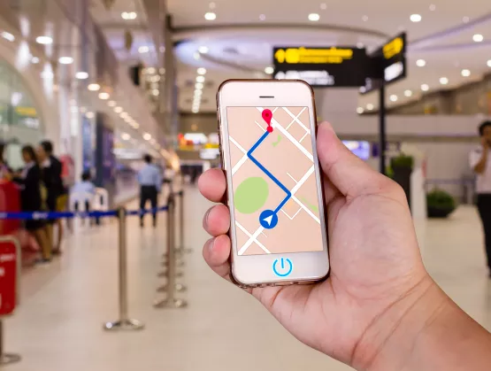
Tracking and localization technologies typically integrate with Wi-Fi and Bluetooth signals to pinpoint the location of people and objects. But what if a venue can’t install beacons or routers, or afford to deploy Wi-Fi or Bluetooth networks? Thanks to a combination of proprietary algorithms, advanced sensor fusion and the natural geomagnetic field, GipStech, a spin-off of Università della Calabria, built an indoor localization and navigation technology platform for accurate localization in the absence of an adequate GPS signal.Ahead of the SEMI MEMS Imaging Sensors Summit, 25 to 27 September 2019 in Grenoble France, Serena Brischetto of SEMI spoke with Gaetano D'Aquila, co-founder and CEO of GiPStech, about sensor fusion, augmented GPS applications and the future of indoor localization. Join us in Grenoble to learn more about GiPStech and meet other MEMS, imaging and sensors experts. Registration is open online.SEMI: Early this year GiPStech completed a test deployment of the first high-precision, infrastructure-free navigation system at Tokyo Shinjuku metro station in Japan. This is the busiest transportation hub globally! What were the main challenges you faced and how did your technology enable such a highly complex indoor localization?D'Aquila: As you mentioned, Shinjuku station in Tokyo has been registered in Guinness World Records as the busiest transportation hub globally. With 36 platforms, 200 exits and countless corridors and connections, it is easy to get lost there, especially for foreigners and tourists. On the other hand, this scale and complexity makes it unfeasible and expensive to install Bluetooth or similar infrastructure for standard indoor localization.For this reason, we needed to provide a cost-effective indoor localization technology without installing any kind of artificial supporting infrastructure. Thanks to our GiPStech patented multi-sensor-fusion localization stack and the high density of public Wi-FI networks, it’s possible to determine when passengers are inside the station. The public Wi-Fi networks signals were fused as an additional source in GiPStech's sensor-fusion platform to complement the inertial and geomagnetic engine and deliver very accurate results across the entire station. The tests performed in the station also demonstrated that the localization system can even detect the floors where travelers are walking. Now we are ready to roll out the same setup in other stations and environments.SEMI: You are not the first to pursue infrastructure-free indoor localization, but your technology platform seems to be very accurate in bringing precision, stability and consistency to the user experience. What lead to those advancements and incredible results?D'Aquila: Our key differentiating factors are built in the approach we created after years of research and development. One differentiation, of course, is related to our expertise and know-how about how the geomagnetic field can be used as a driving signal for the localization process.During R D we constructed and patented a modular multi-sensor-fusion software stack to solve any kind of localization problem, mainly in indoor environments. We started from a single-signal approach based on the employment of the geomagnetic field as a localization signal. But, mainly due to the very inaccurate devices chosen to measure the geomagnetic field, such as the smartphones that everyone carries in their pockets, we noticed that this single-signal approach is accurate but not reliable because it is strongly affected by a key weakness – the quality of sensor in the device.SEMI: How long did it take for you to solve this issue?D'Aquila: We started to integrate other signals within a few months after the first field tests related to the employment of the geomagnetic field alone. We also began to develop a software platform that could fuse any signal source (natural or artificial) available in the environment to preserve the reliability and accuracy of the localization system when some of these signals are temporarily affected by poor measurement quality. This is our differentiating factor today. We can re-configure our software platform to provide the best reliability and accuracy with the lowest artificial infrastructure in almost any context – from outdoor in a seamless way to indoor and vice versa.SEMI: GiPStech’s inertial engine is one of your cutting-edge technologies that completes your advanced indoor navigation and localization software stack. How do you see the technology evolving?D'Aquila: The inertial engine was one of our first technology modules mainly developed to enhance reliability, smooth the signals and reduce the computational power requirement of our geomagnetic localization approach.After a while, together with a third party that evaluated the performances of our module, we noticed that this module not only can be used as a self-standing localization technique, but it can also deliver high accuracy mainly in PDR (pedestrian dead reckoning) applications.Today our PDR is itself a black box with embedded subsystems. Besides some filtering modules, it includes a state-of-the-art step detector that detect steps even when the person changes the smartphone position and location (not only in the hands but also in backpacks or pockets) and an advanced step validation module that identifies and rejects fake steps.If you’ve ever used a commercial fitness tracker attached to your wrist, you know that in most cases if you move your arm the device will counts some steps that, of course, are not real. Our step validator solves this problem by detecting only real steps – a very important capability that allows our PDR to be employed as a self-standing inertial navigation system. We developed the PDR with strong attention to maintaining low requirements for the computational power and memory footprint. These additional characteristics makes the PDR very interesting even for a direct integration of the software at the silicon level in modern MEMS sensors.In a nutshell, the ability of MEMS sensors to run directly an embedded software module will drive technology enhancements that will allow some of the functionalities now available through an external application processor, such as those in smartphones, to move to a lower level (in the silicon). This, of course, reduces power consumption while even increasing the number of value-added services, including localization services, that could be built directly on top of the MEMS without requiring external software and/or application processor.SEMI: Do you think indoor localization will be more applicable in the next 10 years in areas such as Smart manufacturing, travel, healthcare, entertainment and retail?D'Aquila: Several market reports and our business development experience lead us to assess which sectors are of greatest interest for the application of indoor positioning technologies. They include the following. Industry (manufacturing logistics) Healthcare (tracking of assets, patients and doctors) Big installations (visit experience for museums, fairs) Airports stations (both for travelers and for resource and operation management) Large distribution (user profiling and influencing of the purchasing behavior) Indoor localization is a key enabling technology. Adoption, mainly in these sectors, was limited by the unfavorable tradeoff between cost and benefits. Our indoor localization technology aims to overcome those tradeoffs to make its adoption much more cost-effective while providing the best possible reliability and accuracy.SEMI: What are your expectations regarding the summit in Grenoble, and for the future of the sensors technology ahead? Where are we heading?D'Aquila: Many sectors would benefit from indoor localization technologies. MEMS, imaging and sensors are driving innovation and explosive demand for transportation, medical, mobile, industrial and other IoT applications. But these devices also constitute the basic building blocks for the development of reliable and affordable localization technologies.In outdoor environments we are pretty covered by the GPS. Indoors, where we spend more than of 80 percent of our time, similar types of services are coming to the market now and becoming more reliable over time.This Summit facilitates the direct interaction between different stakeholders to act at different points in the MEMS sensors value chain. Indoor localization was an emerging technology unrelated to the sensors ecosystem until now. Today, indoor localization must leverage MEMS sensors to be effective and reliable. In the future, localization technologies will be embedded directly in silicon to deliver the best performance at a lower cost to increase their adoption for more applications.Gaetano D'Aquila served as research fellow from 2002 to 2004 at the CNR and as an assistant teacher at the University of Calabria. From 2003 to 2014, he worked in the industry first as a security consultant for Telcos and Banking in Value Team S.p.A. and then as project manager at Infomobility S.p.A., where he coordinated research and development and strategic activities in the automotive and auto insurance industries. In 2014 he co-founded GiPStech and is its current CEO. He has published several papers in scientific journals and has filed for seven patents, three of which have been granted in the U.S. and Europe. Gaetano has a MSc in Computer Engineering and a Ph.D. in Science and Engineering of the Environment, Buildings and Energy from the University of Calabria, Italy.Serena Brischetto is a marketing and communications manager at SEMI Europe.

Read More
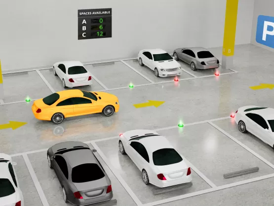
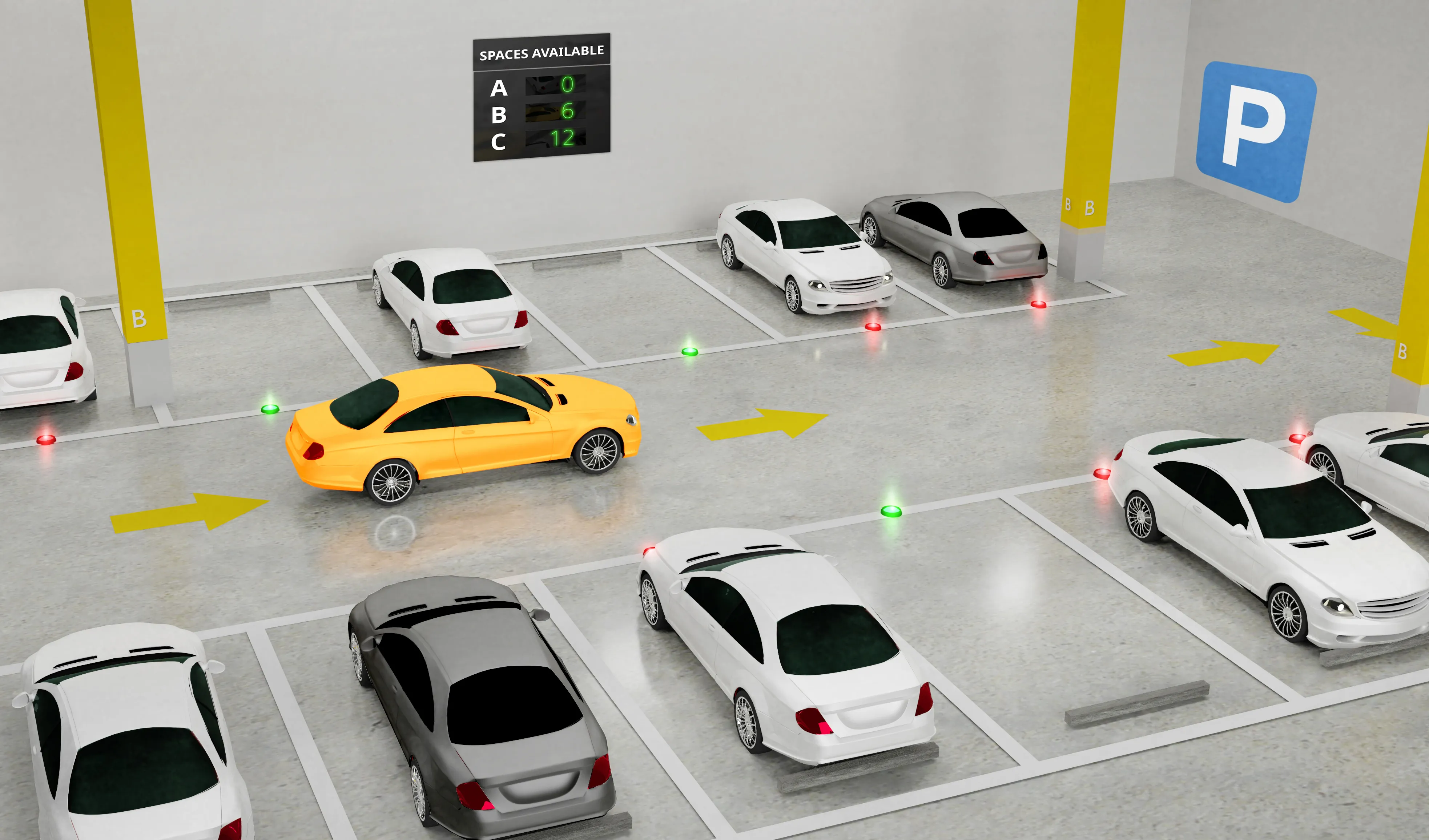
Why Is Smart Parking a Hot Topic? Poorly managed parking resources have a substantial negative impact on cities — one that has been well-documented. According to industry studies, poorly managed parking: Increases Traffic Congestion: 30% of traffic is caused by ongoing circling for parking. Increases Pollution: In Westwood, California, cruising for parking burned 47,000 gallons of gas and generated 730 tons of carbon dioxide in one year. Frustrates Drivers: Urban drivers spend an average of 20 minutes per trip looking for parking. Stifles Economic Opportunities: Traffic congestion cost Americans $124 billion in 2013, and this is predicted to rise to $186 billion by 2030. These problems are getting worse. As a result of growing urban populations, cities account for more than 80% of carbon emissions globally. Unplanned or inadequately managed urban expansion leads to rapid sprawl, pollution and environmental degradation. Due to the lack of parking-space availability, for example, Japan is ranked among the most expensive countries for paid parking. If left unaddressed, poor parking management will continue to plague cities, both large and small. Fortunately, Smart City Internet of Things (IoT) initiatives are helping cities to address their parking issues. IoT to the RescueThere are three key drivers of Smart City IoT initiatives. Cities want to: Improve the overall quality of life and mobility in urban environments Leverage technology to augment and improve existing infrastructure and services that citizens rely on every day Foster both economic and environmental improvements The availability of high-accuracy vehicle detection sensors coupled with affordable, low-power connectivity has enabled a new generation of Smart Parking technology. However, choosing the right Smart Parking solution is essential.High-accuracy vehicle detection sensors can provide valuable data to city planners and parking managers. This information includes: Parking availability Traffic flow Parking occupancy rate and historical data Turnover For parking management to effect change, city traffic managers, parking managers and urban planners need a holistic view of parking availability and usage patterns, and users need real-time information about available parking spaces.Sensors, cameras and communication networks form the basic infrastructure for Smart Parking. To deliver on the promise of IoT and to help cities improve the overall quality of life for residents and visitors, cities need a complete smart parking solution that provides: Accurate real-time vehicle detection and location of available parking spaces – significantly reduces the amount of time spent cruising for parking spaces, giving drivers the precise location of available spaces Connectivity from the sensor to the cloud – facilitates real-time parking data that city planners, parking enforcement and traffic managers can use to reduce traffic congestion Parking applications for cities, parking-lot owners and drivers — enables navigation to available parking and supports mobile payment, streamlining the parking process. Parking applications can also direct traffic enforcement personnel to parking violations as they occur, helping to alleviate traffic bottlenecks, such as double parking in loading zones. Such applications also improve the efficiency of other city services such as public transportation and garbage collection. Complete Smart Parking Solution – Sensor to Cloud (Source: PNI Sensor) To learn how cities are using Smart Parking sensors to improve the services they offer to residents and visitors, come see PNI at SEMI’s 2019 FLEX Japan MEMS Sensors Forum (May 22-23, Toyko, Japan). PNI President and CEO Becky Oh and PNI’s partner, Macnica Networks, will share Smart Parking use cases from innovative cities, corporate campuses and universities (Smart Parking presentation, May 22 from 16:55-17:25). Register for the conference today. For more information about PNI Sensor, visit the PNI Sensor website. Becky Oh is the president and CEO of PNI Sensor. Throughout her 20 years with the company, Ms. Oh has held a range of senior-level positions, from operations to technical business development. She received an M.S. degree in Electrical Engineering from Cornell University and a B.S. in Electrical Engineering and Computer Science from MIT. Ms. Oh holds multiple patents in the area of devices with multi-sensing and reporting capabilities.
Read More