downloadGroupGroupnoun_press release_995423_000000 copyGroupnoun_Feed_96767_000000Group 19noun_pictures_1817522_000000Member company iconResource item iconStore item iconGroup 19Group 19noun_Photo_2085192_000000 Copynoun_presentation_2096081_000000Group 19Group Copy 7noun_webinar_692730_000000Path
Skip to main content
Default Banner Image

semiconductor

The semiconductor industry continues to push the boundaries of innovation, making quality management more critical than ever. To address these challenges, SEMI Quality Benchmarking Consortium (QBC) brings together leading companies to share best practices, benchmark performance, and drive collective improvement across the global semiconductor ecosystem.The latest QBC meeting was hosted by Roberto Lissoni of STMicroelectronics at their Agrate site near Milan, Italy. Representatives from Bosch, GlobalFoundries, Infineon, Micron, NXP, and Texas Instruments gathered for two days of deep discussion and knowledge exchange. (From Right to Left) – Roberto Lissoni (STMicroelecetronics), Giorgio Cesana (STMicroelectronics), Fern Yoon (Texas Instruments), Jens Luepke (Infineon), Mark da Silva (SEMI), Kerstin Nocke (Bosch), John Lepper (GlobalFoundries), Bill Lechten (Micron), Lou Cerra (NXP)With over 5,000 employees, ST’s Agrate facility is the company’s largest in Italy, with a strong commitment to innovation through university collaborations. The site includes both 200mm and 300mm wafer fabs, R D centers, and product development teams. STMicroelectronics Agrate, ItalyThe QBC operates on a “Give-to-Get” philosophy: members must actively contribute survey responses and participate in open discussions to access shared benchmarking data. This meeting focused on four topics: zero defect customer satisfaction, safe launch, knowledge management, and organizational comparisons. Participants presented their approaches, shared lessons learned, and engaged in roundtable discussions to identify best-known methods and address common challenges. Zero Defect and Continuous ImprovementParticipants explored the evolving definition of “zero defect,” emphasizing that it’s not about literal perfection, but about meeting customer commitments and requirements. Quality programs are multi-year, cross-functional initiatives, often embedded in broader operational excellence campaigns. Companies leverage KPIs such as parts per million, cost of nonconformance, and customer satisfaction. They tie these metrics to incentive programs and executive reporting. Continuous improvement is driven by Lean, Six Sigma, and employee engagement, with a strong focus on early detection (“shift left”), cross-functional teams, and digital tools for analytics and feedback. Customer Satisfaction and ScorecardsCustomer scorecards and surveys are central to measuring satisfaction, with processes varying by region and account type. Most organizations use a mix of manual and automated systems to collect, review, and act on scorecard data, supplementing these with relationship and transactional surveys. AI and predictive analytics are emerging tools for anticipating customer feedback and improving proactive management, though data security remains a priority. Safe Launch and Risk ManagementThe QBC companies shared decision criteria, risk assessment methodologies (FMEA, TRA), and enhanced control plans for new products and technologies. Cross-functional collaboration is key, with product quality managers accountable for planning and reporting. Digitalization and integration with manufacturing execution systems (MES) are advancing, and there’s growing interest in leveraging AI for risk assessment and process optimization. Knowledge Management and Lessons LearnedKnowledge management remains a challenge, with most companies relying on distributed databases, expert teams, and informal networks. They are piloting structured lessons learned forums, audit systems, and semantic search tools to improve findability and reuse. Effective knowledge management happens when insights are embedded directly into business processes, supported by continuous review and governance. Looking Ahead: AI, Predictive Quality, and ExpansionThe consortium plans to explore topics such as artificial intelligence, predictive quality management, and secure data sharing through dedicated sessions and working groups, with a focus on practical applications and insights from external subject matter experts.Read about the first QBC meeting hosted by Infineon here. Sarah Shen is Senior Coordinator, MEMS Sensors Industry Group at SEMI.
Read More
The semiconductor and electronics industries are at a turning point. Once defined by efficiency and scale, supply chains now face a convergence of pressures—from geopolitical tensions and climate risks to accelerating innovation cycles. The stakes are higher than ever, but so are the opportunities to reimagine how this global ecosystem operates.The End of “Just-in-Time” as We Knew ItIn 2025, one thing is clear: the old “just-in-time, globally concentrated” supply chain model can no longer carry the industry forward. Trade policies are tightening, export controls are multiplying, and tariff investigations are fragmenting markets that once felt seamlessly connected.At the same time, natural resource risks are mounting. PwC estimates that by 2035, nearly one-third of global semiconductor production could face copper supply disruptions caused by climate change. That figure rises to nearly 60% by 2050 if emissions remain unchecked. Add to this the growing maze of regulatory barriers and import restrictions on raw materials, and the industry faces rising procurement challenges and relentless cost volatility.Demand Isn’t WaitingWhile supply chains struggle with constraints, demand continues its upward climb. Global chip sales are rebounding, driven by innovation cycles in AI, automotive electronics, 5G, and renewable energy. Bringing new manufacturing capacity online takes years. The imbalance is widening, and companies can’t afford to rely on outdated, reactive supply chain models.Resiliency has become mission critical. And as the saying goes: you can’t respond to risks you can’t see. Guesswork isn’t a strategy—especially when disruptions are systemic.Fragility in a Fragmented EcosystemSemiconductor production is specialized and geographically fragmented. A disruption at a single node—whether a mine, a fab, or a logistics hub—can ripple through the ecosystem in days or even hours.Recent shocks have only reinforced this fragility:Trade restrictions are pushing manufacturers to rethink supply chain design.Climate change is endangering raw materials like copper and quartz, both highly water- and energy-intensive to produce.Market volatility is being driven by the explosive rise of AI and data center demand.The lesson is simple: resilience is no longer optional—it’s an existential requirement. And the path to resilience runs through visibility, agility, and collective intelligence.Real-Time Intelligence: From Luxury to NecessityIn today’s environment, quarterly or even monthly reporting cycles are dangerously slow. By the time a shortage, tariff, or logistics reroute appears on the radar, the window to act may have already closed. The cost of waiting—or doing nothing—is steep, and the damage can be lasting.Real-time data and AI-driven insights aren’t “nice-to-have” tools anymore. They are strategic imperatives for supply chains under constant stress. They allow companies to anticipate risks, respond faster, and align more effectively with partners across the ecosystem.Collaboration Is the New CurrencyNo company can go it alone. A chipmaker depends on its suppliers, just as a rare earth miner depends on transport partners. The global supply chain is a living system—and its resilience depends on the strength of its interconnections.Deeper supplier relationships, visibility into Tier 2 and Tier 3 suppliers, and shared intelligence on geopolitical and regulatory shifts are all critical. Resiliency isn’t built in silos; it’s forged through collective action.Building the Future TogetherThe semiconductor and electronics industries stand at the threshold of a new era—one of collective risk but also shared potential. Companies that embrace transparency, real-time intelligence, and collaboration will not just survive shocks, but emerge stronger, more agile, and better prepared to lead.In this new chapter, collaboration is the currency of resilience.That’s where Conductor™ comes in: a real-time intelligence platform built to help industry players anticipate, adapt, and act – together. Conductor weaves all those threads together, delivering not just data, but a shared situational awareness, helping the industry to think and act as a system rather than a collection of silos.What Conductor Enables - and What It Could Lead ToSmarter, faster decisionsA platform like Conductor, which uses near real time data, AI-powered news and alerts, and community-driven insights, turns reactive “damage control” into proactive “risk management.”By bringing together cross-segment, critical KPIs, curated AI news, expert analysis, and peer-community intelligence, Conductor helps teams understand what’s happening now, assess the likely impact on their business, and decide how to respond - faster, and with more context.Over time, this could shift the default mode of the industry from “fire-fighting” to “anticipatory steering.”A more adaptive supply chainAs more organizations adopt the platform, the collective visibility improves. Conductor can power scenario planning, enable early warning systems, and foster agile “micro-pivot” strategies: reroute logistics, adapt sourcing, or reallocate production before a disruption becomes a crisis.New models of ecosystem resilienceWith consistent, shared intelligence, industry players can identify common vulnerabilities and coordinate mitigation for mutual gain. Over time, this could lead to more resilient operations through diversified sourcing strategies, and even shared contingency mechanisms.In short: Conductor is a building block toward a more distributed, more transparent, more resilient global semiconductor ecosystem.Accelerated innovation cyclesWhen the risk of disruption is better managed, companies can operate with more confidence, investing in new capacity, experimenting with new chip architectures, or integrating new markets more aggressively. Technology diffusion accelerates when the fear of “what-if” is reduced.Where We Go From HereConductor is already in early-access pilot phase, and feedback from the SEMI Supply Chain Management Initiative’s Industry Advisory Council is actively shaping its evolution.As adoption spreads, network effects will increase the platform’s predictive power, making it more valuable for everyone involved.In an industry that’s increasingly defined by fast change and high stakes, tools like Conductor shift the balance: from reactive scramble to informed strategy, opaque fragility to visible resilience, and from isolated action to ecosystem collaboration.The future of supply chain resilience starts here. Sign up for early access to Conductor today and help drive the new era of trade.Talal Abu-Issa is Co-CEO and Co-Founder of Beebolt.Krish Dharma is Strategic Advisor, SEMI Supply Chain Initiative.
Read More
The semiconductor industry is at the forefront of technological innovation, with rapid advancements in recent years. As a result, the need for high-quality products and technologies has become increasingly important. To address this challenge, SEMI has launched the Quality Benchmarking Consortium (QBC), a new initiative dedicated to advancing quality best practices across the global semiconductor industry. Quality is a fundamental requirement for all semiconductor products and technologies. Over the past decade, state-of-the-art quality practices have evolved significantly to keep pace with rapid innovation and technological advancements. However, new challenges have emerged, including qualifying increasingly complex systems, advanced packaging and 2.5/3D integrated systems, and the growing role of AI/ML in manufacturing. Company-to-company benchmarking is a powerful tool for enhancing quality practices. By sharing information, input, and feedback, companies can establish best-known methods (BKMs) to elevate quality best practices across the entire industry. This approach can save time and money, while also driving innovation and improvement. The QBC is open to multinational corporations, including device manufacturers, fabless device makers, and foundries, that ship over 100 million units per year and have a high-caliber quality organization. The consortium operates on a "Give-to-Get" philosophy, requiring members to actively participate in discussions and activities. Permitted topics for discussion include working processes, management systems, approaches, and KPIs, driven by global customer trends or internal development. However, off-limit topics include IP and patent-protected quality technical solutions embedded in technologies, packages, design, testing, and software.Figure 1: (From Right to Left) - Georg Talut (Global Foundries), JensLuepke (Infineon), Rutger Wijburg (Infineon), Roberto Lissoni (ST Microelectronics), Marcus Richter (Bosch), Bill Lechten (Micron), Georg Georgakos (Infineon) Mark da Silva (SEMI)The first in-person consortium meeting was hosted by Infineon at its Campeon campus in Munich, Germany, and brought together representatives from Infineon, STMicroelectronics, Bosch, GlobalFoundries, and Micron. The event commenced with a warm welcome from Jens Luepke, Senior Director of Quality Management at Infineon, who introduced the company's global operations, history, and employee support initiatives. Rutger Wijburg, COO at Infineon, outlined the company's strategic focus on decarbonization, digitalization, and revenue growth across key business segments. He shared Infineon's investments in new facilities and emphasized the critical role of quality management in navigating industry challenges such as accelerated qualification cycles, increasing product complexity, and mounting cost pressures. Wijburg encouraged participants to leverage insights from the consortium to enhance quality processes within their own organizations and deliver greater value to customers. In preparation for the first in-person meeting, consortium members were organized into three teams, each addressing a core area of quality management: Design Quality (Robustness), (Quality) Organization Structure and Supplier Quality Management.The Design Quality session at the QBC focused on integrating design quality into the New Product Introduction (NPI) process, covering topics such as accountability, quality metrics, and bug tracking systems. Subject matter experts shared strategies on design quality methodologies, metrics, and verification processes, including the use of generative AI. The Organization Structure session shared existing quality organizational structures and management strategies, including reporting lines, functional responsibilities, and employee training programs. The Supplier Quality Management session addressed procurement practices, inventory management, and supplier qualification, with companies sharing best practices for mitigating material fluctuations and advancing sustainable procurement. Overall, the sessions aimed to share knowledge and best practices to improve design quality, organizational structure, and supplier quality management in the semiconductor industry.The meeting concluded with formal nomination of Roberto Lissoni (STM) and Jens Luepke (Infineon) as QBC co-chairs. The meeting wrapped up with a call to action: Expanding the consortium, planning the next in-person meeting (targeted July’25), and amplifying industry engagement. We're excited to welcome new members to the Quality Benchmarking Consortium! If you're interested in joining the conversation, contact Mark da Silva ([email protected]) or Sarah Shen ([email protected]) to learn more.Sarah Shen is Senior Coordinator, MEMS Sensors Industry Group at SEMI.
Read More
The drive to scale nodes towards physical limits, known as "More than Moore," and the adoption of 3D architecture in chip integration strategies for advanced logic and memory applications has led to unprecedented demand for high-quality dependable materials solutions. With the aid of digital solutions, the process is expedited with higher quality and efficiency.SEMI spoke with Thorsten vom Stein, Director, Head of Process Design Semiconductor Materials at Merck KGaA, Darmstadt, Germany, about how materials innovations and advanced packaging can contribute to smarter supply chain solutions for a sustainable ecosystem.More insights into key aspects of 3D architecture in chip integration and heterogeneous integration will be shared at the Advanced Packaging Conference (APC) during SEMICON Europa 2024, Nov. 12-15 in Munich, Germany. Registration is open.SEMI: What makes the digitalization of chemical process design for semiconductor materials manufacturing so challenging at a technology level? Vom Stein: The primary challenge in digitalization of process design is achieving data rich experimentation and design flexibility from the start. When we begin the process design for a novel material solution, the freedom of design needs to be very high for optimal outcomes. For example, to identify the best sequence of unit operations to achieve best process intensification, do we need a distillation or extraction after the reaction to meet the purity requirements? At the same time, the samples from these early process trials need to have purity levels and process reliability standards for high-volume manufacturing of routine production in order to meet the requirements of our customers’ leading-edge chip integration strategies. We address this need by executing data rich experimentation starting with first trial, and thereby establish “production ready” data density in the lab.To avoid confining our design space, we therefore need highly “sensorized” and automated modular lab equipment that can give us the data density we need and flexibility at the same time.SEMI: Are data-driven approaches also applied to streamline manufacturing processes? Vom Stein: Yes, data-driven approaches are key to driving cost, quality, process reliability and sustainable excellence. As we scale up from lab experiments to high-volume manufacturing—often times increasing volumes by two or three orders of magnitude—we scale the process model virtually ahead of its physical twin to de-risk these major scale-up steps. An example of this is simulating the effect of reactor geometry on the impurity profile.Establishing this handshake between the physical asset and the process model early in the development has a lot of benefits for sustained cost efficiency of the future manufacturing process. For instance, it allows for optimization of yield and cycle times to the existing asset infrastructure. Furthermore, we can achieve quality reliability critical to our customers by establishing end-to-end correlation models that link the quality of incoming raw materials to finished good impurity profiles.Finally, we can achieve the lowest possible carbon footprint and minimize waste streams and energy intensity via process intensification by matching the unit operation sequence to the specific thermodynamics and kinetics of the process.SEMI: How can advanced packaging contribute to the pursuit of net zero? Vom Stein: Ultimately in a successful process design, we aim to achieve the maximum yield of value-added product with minimal input of resources and raw materials. So, there is an intrinsic synergy between highly intensified processes and their carbon footprint. The digitalization of process design allows us to track the CO 2 footprint during every iteration of the design. Establishing this tracking as a routine design KPI is one of the key initiatives to drive net zero semiconductor material solutions.In addition, advanced process design is a key enabler for circular value streams. We are currently working on multiple projects to recycle waste streams and re-feed them as raw materials in our processes. We are also exploring how our chemical process technology can aid our customers’ recycling efforts such as reusing lithography cleaning solvent waste streams.SEMI: In your previous talks, you emphasized the importance of diversity, equity and inclusion (DE I). How is this related to the digital revolution? Vom Stein: In the not-so-distant past, my team consisted mainly of process chemists and engineers. Now, we are working with data scientists, model developers, automation experts and many more substance matter experts on our projects. This work requires an inclusive culture to maximize the impact of these diverse sets of insights and disciplines.We also must acknowledge that, in many instances, we are exploring unchartered territory that requires a “leap of faith” culture trusting in digital models. Imagine, for example, a production plant director who is used to a stepwise physical scale-up, now being onboard with skipping physical scale-up steps by using predictive process models. It takes time to really establish a trust in the “power of data.” This type of culture is championed at Merck KGaA, Darmstadt, Germany on all levels: from CEO to the production operator. Our DE I Report showcases how we continuously build belonging for over 64,000 employees across the globe.SEMI: Merck KGaA, Darmstadt, Germany is a key contributor to semiconductor innovations. How important is it for Merck KGaA, Darmstadt, Germany to collaborate with other industry leaders to achieve goals in matters such as sustainability and DE I? Vom Stein: Collaboration with our customers and OEM partners is a key piece of achieving the molecular precision necessary to drive technology evolution that serves as the backbone to society. More and more, we need to link our material solution manufacturing process to the process parameters of the tools in the fab, ultimately improving the chip yield of our customers. To transition from the nanometer era to the angstrom era, we must establish these process correlations end to end along the value chain, which is why we are heavily engaged on our Athinia collaboration framework.Besides technology enablement, sustainability is the next avenue where cross value chain collaboration is a must to lower the CO 2 and energy footprint of our industry. To this end, we have started a joint program with Intel on AI-enabled sustainable semiconductor processes.The importance of industry collaboration is why I was so honored to participate at SEMICON Europa together with representatives from leading companies.SEMI: What did enjoy about SEMICON Europa 2023 that you would like to experience again in 2024? Vom Stein: I was really impressed by the SEMICON Europa 20 Under 30 recognition program launched during the show. The program honored the brightest young leaders who have demonstrated success in their careers in the microelectronics supply chain. We were very happy with the acknowledgement of one of our brightest minds at Merck KGaA, Darmstadt, Germany, Balazs Bordas, Digital Twin Implementation Lead. He has been instrumental for many of our pioneering efforts in this space.Such recognition programs are very important for our industry and can make a significant difference in the perception of the semiconductor industry and its ability to motivate and attract more talent. I personally hope to see similar programs in the years to come.Additional resources:Learn more about diversity and inclusion at Merck KGaA, Darmstadt, Germany.Learn more about Merck’s KGaA, Darmstadt, Germany modular lab automation approach.Merck KGaA, Darmstadt, Germany sponsored SEMICON Europa and SEMI Advanced Packaging Conference in 2023. Thorsten vom Stein is Director, Head of Process Design Semiconductor Materials at Merck KGaA, Darmstadt, Germany. Based in Darmstadt, Germany, he holds a PhD in Chemistry from the RWTH Aachen University and has extensive experience in Catalysis, Materials Science, Process Development and Value Chain Innovation.Serena Brischetto is Director of Marketing and Digital Engagement at SEMI Europe.
Read More
Silicon carbide (SiC), with its wide band gap and high thermal conductivity, is increasingly favored for semiconductor power applications across several fast-growing industries. Its ability to operate at higher voltages and frequencies enables significant efficiency gains, particularly in e-mobility, where SiC offers key advantages in size, weight, and speed compared to traditional silicon-based power devices.However, as promising as SiC is, the industry still faces critical challenges in scaling to meet growing demand. Key barriers include cost, reliability, and manufacturing capacity, all of which must be addressed for SiC to fully mature.SEMI spoke with Entegris Senior Director - Advanced Technology Engagements, Office of the CTO Mark Puttock, Ph.D., to discuss the challenges of scaling SiC power chip manufacturing from a material supplier’s perspective. Puttock shared insights ahead of his presentation at the Entegris session, Cultivating a Thriving SiC Market: Tackling Key Challenges Across the Value Chain, taking place on November 14, 2024, at SEMICON Europa in Munich, Germany. Don’t miss the opportunity to engage with experts from Entegris and other industry leaders. Registration is now open. SEMI: Global megatrends like environmental crises and AI drive the necessity for SiC power semiconductors. What is the current status? Puttock: The increasing demand for efficient power electronics — fueled by global megatrends such as vehicle electrification, environmental de-carbonization, and the rise of power-hungry AI chips — drives the necessity of wide bandgap semiconductors. SiC offers advantages of weight, size, and speed over traditional silicon (Si) solutions, which are particularly vital in automotive applications 600V and above. However, SiC chip manufacturing has not reached the maturity of silicon-based processing. Greater maturity will help reduce costs, which will accelerate adoption in the market.SEMI: What are the main challenges in scaling SiC?Puttock: Challenges in scaling SiC power chip manufacturing to high volumes are not surprising. That’s because high volume producers have not been operating long enough to resolve early-stage issues. From a material perspective, SiC is more challenging to manage compared to Si. The challenges we identify include:Chemical Mechanical Planarization (CMP): SiC is nearly as hard as diamond and significantly harder than Si, making it challenging to achieve a high removal rate while maintaining both planarity and low defectivity. This step is crucial toward the end of the wafering process and before the epitaxial growth of device layers.Handling: SiC is more brittle than Si, making it more susceptible to damage or breakage.Implantation: SiC is more difficult to implant than Si, requiring higher temperatures and the use of aluminum instead of boron as a P-type implant species. Additionally, it is a significant challenge to achieve a reliable aluminum source with a long and stable lifetime.Thermal Processing for Wafer Growth and Epitaxy Processes: SiC processes run hotter than Si ( 2000° C for wafering, 1500° C for epitaxial growth), demanding resilient chamber parts to achieve good lifetimes.Sustainability: Because SiC is extremely hard, the CMP process requires significant amounts of slurry. Improving slurry recycling and wastewater management continues to be a challenge.On October 29, we will address these issues in our webinar, “Challenges in Scaling SiC Power Chip Manufacturing: A Material Supplier's Perspective” This session will provide valuable insights and considerations for advancing maturity in high-volume SiC power chip manufacturing. SEMI: Can you elaborate on the challenges associated with CMP for SiC wafers? Puttock: SiC wafers are challenging to process, requiring specialized materials and methods compared to traditional silicon. Defects in the SiC wafer crystal during non-optimized CMP processing can propagate into the device epitaxial layers. This leads to yield loss, increased electrical resistance, reduced performance, and wasted power.SiC wafers must be cut, ground, lapped, and polished to create the necessary surface properties before depositing active layers. As the demand for these devices grows, optimizing the CMP process is essential to ensure the desired surface quality and planarity required for device fabrication. For a deeper understanding of these challenges, we recommend downloading our latest white paper, “Solving CMP Challenges in High-Volume SiC Production,” which covers:Achieving maximum smoothness with high removal ratesReducing the total cost of ownership Optimizing CMP slurry and pads for the unique wafer chemistry and topology of SiC wafersSEMI: What do you mean by optimizing slurry for SiC CMP?Puttock: CMP slurry typically consists of abrasive nanoparticle powder dispersed in a chemically reactive solution. The objective is to achieve a smooth, defect-free surface (less than 1 A Ra) with a high removal rate (greater than 7 µm/m).Traditionally, achieving high removal rates and smooth surfaces required two separate slurries. This approach sometimes forced SiC wafer manufacturers to choose a defect-free surface over a faster, more efficient CMP process, depending on their fab capabilities. Today, optimization allows SiC wafer manufacturers to achieve both high polishing capacity and good final surface quality using a single slurry.Additionally, while the slurry is the most critical part of the CMP process, the pad must be compatible with the application. This ensures the desired planarity while also preventing scratches or contamination of the SiC wafer surface. Research shows that optimized thermoplastic polyurethane CMP pads outperform traditional thermoset polyurethane pads. The optimized pads minimize surface damage and enhance removal rates due to their bulk hardness.SEMI: What are the future challenges for SiC devices? Puttock: SiC devices are increasingly favored for their superior energy efficiency and reduced environmental impact. However, the SiC manufacturing process presents challenges due to its high-temperature operations, which consumes significant amounts of energy and shortens the lifespan of chamber components. To address this, improving efficiency in these processes will be crucial in the coming years.Recycling is another important challenge. For example, CMP slurries present an opportunity for water recycling and conservation. At Entegris, we are committed to this issue and are actively collaborating with key industry players to enhance material circularity and prioritize sustainability in our new product development.SEMI: How is Entegris contributing to advancements in SiC technology, and what initiatives or partnerships do you have planned for the near future? Puttock: Entegris is an active member of the SEMI Global Automotive Advisory Council (GAAC) and participates in a working group focused on SiC with key industry leaders such as Volkswagen, BMW, Porsche Consulting, onsemi, Infineon, STMicroelectronics, and others. Our engagement spans the entire semiconductor supply chain, collaborating with integrated device manufacturers and original equipment manufacturers in fabs worldwide. Additionally, we recently announced our latest long-term agreement with onsemi, which underscores our commitment to advancing SiC technology.SEMI: What are your expectations regarding your participation at SEMICON Europa? Puttock: SEMICON Europa is a unique platform to connect with the semiconductor and automotive ecosystems. Last year, we organized a highly successful SiC session in collaboration with SEMI at both SEMICON West and SEMICON Europa, focusing on “Connecting the Automotive Ecosystem Towards More Mature SiC Manufacturing.”This year, we will continue the discussion with industry leaders during our session, “Cultivating a Thriving SiC Market: Tackling Key Challenges Across the Value Chain.” Our goal is to provide insights and propose solutions that will enable SiC power chips to achieve their anticipated role in future technology ecosystems.We will present alongside Porsche Consulting, and the talks will be followed by a panel discussion that will explore the current state and future prospects of SiC technology in power electronics. We invite visitors to join us at the Executive Forum on Thursday, November 14, from 1:40 – 3:00 p.m. and to visit us at Silicon Saxony booth 219 in Hall C1.About Mark PuttockMark Puttock, Ph.D., is the senior director of advanced technology engagements in the office of the CTO at Entegris. He has worked in the semiconductor industry for over 30 years with a background in physics and plasma processing. As a team member of the Entegris CTO office since 2014, Mark has followed technology trends and collaborated with Entegris’ global product development teams to develop timely and differentiated new materials, chemistries, and components for all the world’s semiconductor manufacturers. Maria Daniela Perez is Communications Manager at SEMI Europe.
Read More
Micron, one of the top three memory semiconductor companies, reported solid results for the fourth quarter of fiscal 2018 (June to August) to extend a multi-quarter string of strong growth. However, the company’s mediocre guidance for the current quarter has raised concerns that memory demand will start to slow.To shed light on this super memory cycle, which began in the second half of 2016, this article examines correlations among the top three memory suppliers’ sales revenue, quarterly inventory levels, World Semiconductor Trade Statistics (WSTS) market data, and memory fab equipment investments reported by SEMI.The Memory Inventory Cycle Index, which is based on financial data reported by Samsung, SK Hynix and Micron, is the difference between the year-over-year growth rates of sales (or shipments) and inventories. The index explains business cycle fluctuations such as expansions and contractions, trending up in expansions and declining in contractions. Figure 1 shows both historical Micron sales (blue dotted line) and the quarterly Memory Inventory Cycle Index (black solid line). To minimize seasonal fluctuations, both were calculated based on a four-quarter moving average of sales and inventories. Figure 1. Memory Inventory Cycle Index Compared to Memory Sales* Remarks1) Memory Inventory Cycle Index = YoY growth rate of memory sales revenues - YoY growth rate of memory total inventoris value on a four quarters moving average.2) Calculated memory sales and inventoris are based on Samsung, SK Hynix, and Micron public announcements.3) South Korea Won were converted to US$ based on the quaterly average value released by FRED.4) Companies’ sales data were calculated based on 4-quarter moving average.5) Company data complied by SEMI. As shown in Figure 1, the Memory Inventory Cycle Index has been declining since peaking in the fourth quarter of 2017, mirroring the previous two contractions – in 2010 and 2014 – in which memory sales slowed or stagnated after four quarters of the index decline. Accordingly, if this relationship holds between the Memory Inventory Cycle Index and sales, Micron’s sales will slow in the coming quarters and is consistent with Micron’s guidance for the current quarter. Moreover, the index suggests that the sum of three companies’ sales (the solid red line) will exhibit a similar trend of decreased growth in the coming quarters, which will impact the annual growth rate of global memory sales.WSTS recently increased its 2018 forecast for memory sales to 30.5%, up from 26.5% projected in June of this year. However, the 3-month moving average of memory sales shows that memory sales already increased by 48% YoY in the first half of the year, which means growth is expected to be lower in the second half of the year. Other signs pointing to a weaker end to the year include front-end equipment investments by the top three memory suppliers. SEMI is modeling an annual increase of only one percent for the year for these suppliers, with spending down 23% in the second half relative to the first half of the year.Figure 2 shows the historical trend of the Memory Inventory Cycle Index, the YoY growth rate of memory sales, and YoY memory fab equipment investments. The Memory Inventory Cycle Index increased faster than memory sales and fab equipment investments in the past two cycles. In the most recent memory cycle, these three indexes are moving in tandem, each peaking in the fourth quarter of 2017. Figure 2. Memory Inventory Cycle Index, Memory Sales and Memory Fab Equipment Investments* Remarks1) Both sales and memory fab equipment investments data were calculated based on 4-quarter moving average to minimize seasonal fluctuation.2) All data are from SEMI, except memory sales (WSTS) While overall memory sales continue to be strong this year, memory ASPs have shown signs of weakening right after the inventory index peak. NAND flash ASPs have been trending downward since the first quarter of 2018. With the recent inventory correction and short-term CPU shortage, DRAM ASPs are expected to soften in the fourth quarter of 2018. The looming memory market slowdown has memory makers adjusting their capacity expansion plans for the rest of this year. Some new capacity additions, especially for DRAM, have been pushed out to 2019. The memory inventory cycle index has to some extent foretold the slowdown of the memory market. In the second and final part of this article, we will discuss the correlation between the Memory Inventory Cycle Index and China’s semiconductor sales and Purchasing Managers Index. We will also look at the increasing level of memory inventory in the past few quarters and its composition including Work-in-Progress and Finished goods. Clark Tseng is director and Sungho Yoon is senior market research analyst in Industry Research and Statistics at SEMI. SEMI World Fab ForecastFor the latest worldwide memory fabs forecast including company details, please see the SEMI World Fab Forecast. The report includes quarter-to-quarter fab data from planning to production for both DRAM and NAND Flash companies.
Read More
Last week, more than a dozen senior semiconductor executives traveled to Washington, DC for the first-ever Fall Washington Forum. The SEMI Washington Forum, a venue for SEMI members to educate lawmakers about the industry, focused on action against China, both in the form of tariffs and export controls.Our industry is global, and companies rely heavily on trade. In 2017, more than 90 percent of equipment made in the United States was exported. Because of this dynamic, the United States holds a nearly $9 billion trade surplus in this industry. SEMI supports trade policies that open foreign markets. In the meetings, the executives expressed deep concern that the tariffs would inflict deep damage to the U.S. economy, including to SEMI members. Estimates suggest that the Sec. 301 tariffs (and the Chinese retaliatory tariffs) will cost semiconductor companies more than $700 million annually, dramatically increasing the cost of doing business. These tariffs also threaten U.S. technological leadership. The United States has led innovation for decades. However, by pursuing policies that limit market access opportunities, company-led R D and innovation will slow, which, in turn, will curb further export potential. SEMI companies also stressed that because of the blunt application of these tariffs, this action will actually hurt U.S. companies as much as it hurts their Chinese competitors. Indeed, about 40 percent of imports in our sector from China are from U.S. or other non-Chinese companies. Further, the semiconductor industry relies on a vast network of supply chains, which have been built and qualified over the course of years. A fundamental revamp of supply chains is simply not feasible. This would be expensive, time-consuming, and resource-intensive. With a growing number of policy issues that are central to and could have significant impact for semiconductor companies, SEMI hosted its first ever Fall Washington Forum for members of its North American Advisory Board (NAAB). SEMI also invited several other industry executives. In total, 14 senior industry executives, including representatives from equipment manufacturers, component suppliers, and materials providers, attended the Fall ForumDuring the two days of meetings, SEMI met with several senior Administration officials to better the policies being enacted and considered as well as encourage all parties to not impose barriers to commerce, which would severely impact the semiconductor industry. SEMI also met with Members of Congress and their staffs on this issue. All told, attendees at the Fall Forum had more than 15 meetings with policymakers, reflecting the great impact of public policy on SEMI members companies. At a time when the stakes for the industry could not be higher, direct engagement with lawmakers is critical. The Washington Forum offers an incredible opportunity for members to better understand the impact of key public policy issues and gain firsthand experience in influencing policy and helping lawmakers better understand the industry.If you are interested in learning more about the SEMI Washington Forum or SEMI’s public policy program, please contact Jay Chittooran by email at [email protected].
Read More
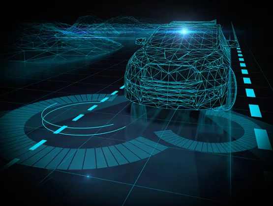
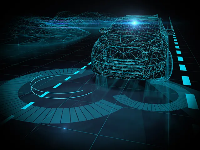
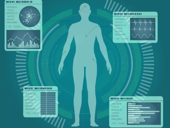
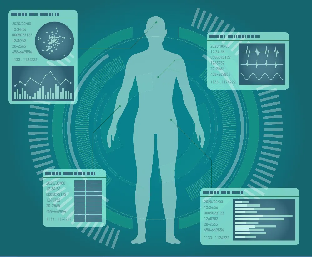
Sensors are inextricably linked to the future requirements of partially and fully autonomous vehicles. From highly granular dead-reckoning subsystems that rely on industrial-strength gyroscopes for superior navigation to more intelligent and personalized cockpits featuring intuitive human machine interfaces (HMIs) and smart seats, new generations of partially and fully autonomous cars will use sensors to enable dramatically better customer experiences.Dead reckoning, or, where am I, exactly? Dead reckoning is the process of calculating one’s current position by using a previously determined position, and advancing that position based upon known speeds over a time slice. As a highly useful process, dead reckoning is the basis for inertial navigation systems in aerospace navigation and missile guidance, not to mention your smartphone.Today’s best-in-class MEMS gyroscopes can offer 30-50 cm resolution (this is the yaw rate drift) over a distance of 200 meters — a typical tunnel length where a GPS signal is lost. For semi-autonomous (L3) or autonomous (L4, L5), the locational accuracy is well below 10 centimeters; that’s an accuracy usually reserved for high-end industrial or aerospace gyroscopes with a raw bias instability ranging from 1°/h and down to 0.01°/h. These heavy-duty gyros command prices from $100s up to $1000s. Current performance levels of different gyroscopes by application and performance measure in terms of bias drift (IHS Markit). This poses an interesting potential opportunity for both industrial-performance MEMS-based gyroscope sensor-makers, such as Silicon Sensing Systems, Analog Devices, Murata, Epson Toyocom and TDK InvenSense, and for broader-based sensor component-makers such as Bosch, Panasonic, STMicroelectronics, and TDK (InvenSense and Tronics).While MEMS can master performance, size and low weight, cost remains the challenge. The fail-operational mode requirement for autonomous driving will accommodate higher prices, at least in the beginning, probably in the $100+ range at first, even for the relatively low volumes of self-driving cars anticipated by 2030. Nonetheless, automotive volumes are very attractive compared to industrial applications and offer a lucrative future market for dead-reckoning sensors.Your cockpit will get smarter Automakers are banking on the idea that people like to control their own physical environment. Interiors already feature force and pressure sensors that provide more personalized seating experiences and advanced two-stage airbags for improved safety. In some vehicles, automakers are using pairs of MEMS microphones for noise reduction and image or MEMS infrared sensors for detection of driver presence. Eventually, we might see gas sensors that monitor in-cabin CO2 levels, triggering a warning when they detect dangerous levels that could cause drowsiness. These smart sensors would then “tell” the driver to open the window or activate an air-scrubbing system in a more complex solution. While today’s CO2 sensors are still relatively expensive, we may see them designed-in as lower-cost versions come to market.Future cockpits will need to go beyond such concepts in the lead-up to fully automated driving. Seats could contain sensitive acceleration sensors that measure heart and respiration rates as well as body movement and activity. Other devices could monitor body humidity and temperature.We need look no further than Murata, a supplier initially targeting hospital beds with a MEMS accelerometer as a replacement for pulse oximeters. That same Murata accelerometer could be placed potentially in a car seat to detect heart rate. It’s not the only way to do this: another sensing approach for heart-rate measurement comprises millimeter wave radiation, a method that can even look through objects such as books and magazines.Augmenting sensor-based body monitoring, automotive designers will use cameras to fuse information such as gaze direction, rate of blinking and eye closure, head tilt, and seat data with data gathered by sensors to provide valuable information on the driver’s physical condition, awareness and even mood. Faurecia’s Active Wellness concept—unveiled at the 2016 Paris Motor Show—proves that this technology might be coming sooner than we think. Active Wellness collects and analyzes biological data and stores the driver’s behavior and preferences. This prototype provides data to predict driver comfort based on physical condition, time of day, and traveling conditions, as well as car operating modes: L3, L4 or L5. Other features such as event-triggered massage, seat ventilation and even changes in ambient lighting or audio environment are possible. Faurecia’s “cockpit of the future,” announced at CES 2018. (Faurecia) Meanwhile, there are other commercial expressions of more advanced HMI as well as plenty of prototypes. Visteon’s Horizon cockpit can use voice activation and hand gestures to open and adjust HVAC. Capacitive sensors are already widely used for touch applications, and touchless possibilities range from simple infrared diodes for proximity measurement to sophisticated 3D time-of-flight measurements for gesture control.Clearly, automotive designers will have a lot more freedom with HMI in the cabin space, providing a level of differentiation that manufacturers think customers will appreciate—and for which they will pay a premium.Managing sensor proliferationResearchers are investigating ways to solve the issue of high-functionality vehicles containing myriad sensing inputs, i.e., when we have so many sensing inputs, designers must address wiring complexity and unwanted harness weight. Faurecia, for example, is considering ways to convert wood, aluminum, fabric or plastic into smart surfaces that can be functionalized via touch-sensitive capacitive switches integrated into the surface. These smart surfaces could reduce the explosion of sensing inputs, thereby diminishing wiring complexity. With availability from 2020, Faurecia’s solutions are approaching the market soon.Beyond functionalized switches, flexible electronics and wireless power sources, and even energy harvesting (to mitigate power sources), could provide some answers. Indeed, recent research has shown that graphene-based Hall-effect devices can be embedded in large-area flexible Kapton films, and eventually integrated into panels. OEMs such as Jaguar Land Rover are interested in such approaches to address the downsides of electronics and sensor proliferation, especially in luxury vehicles. While smart surfaces would represent a big change in sensor packaging and a disruption in current semiconductor processes, they remain a long way from commercial introduction.By 2030 or thereabouts, fully autonomous cars that detect our mood, vital signs and activity level could well be available. Cabins could signal us to open the window if CO2 levels become dangerous. HVAC systems could increase seat ventilation or turn up the air conditioning (or the heat) based on our body temperature. Feeling too hot or too cold in the cabin could become a thing of the past, at least for the driver, whose comfort level is the most important! We could feasibly feel more comfortable in the car than in our office, our home or at the movies. Perhaps our car will become our office, our entertainment center and our home away from home as we take long road trips with the family, without a single passenger uttering, “Are we there yet?” Bio: Richard Dixon, Ph.D., is a senior principal analyst for MEMS research at IHS Markit and author of more than 50 MEMS-related consulting and market research studies. He is a renowned expert on automotive MEMS and magnetic sensors used in safety, powertrain and body applications. Along with supporting the overall activities of the MEMS and sensors group, his responsibilities include the development of databases that forecast the markets for more than 20 types of silicon-based sensors in more than 100 automotive applications. In addition, he has supported organizations with future scenarios for sensors in cars and has supported many custom projects for companies in the automotive supply chain.In his prior post at Wicht Technologie Consulting (WTC), Dixon was a senior MEMS analyst where he led research on physical sensors and was the co-author of the NEXUS Task Force Report for MEMS and Microsystems 2005-2009. He has also led commercialization and road-mapping activities on European Commission-funded technology projects, including detailed MEMS chip cost analysis studies.Dixon worked previously as a journalist in the compound semiconductor industry and has five years of experience as a technology transfer professional at RTI International, where he provided business and market intelligence for early-stage technologies.Dixon graduated from University of Greenwich with a degree in materials science and earned a doctorate from Surrey University in semiconductor characterization. He speaks English and German.For more information, visit https://technology.ihs.com/Categories/450486/mems-sensors. ___________________________________________________________________________________________________ Want to hear more from IHS Markit on MEMS and sensors devices and their applications? Top thinkers from IHS Markit will be speaking at upcoming SEMI events. Register today!Disruption in the authentication sensor market Manuel Tagliavini, Principal Analyst, MEMS Sensors, IHS Markit Autonomous and Electric Cars: What's in for Conventional MEMS SensorsJeremie Bouchaud, Director and Senior Principal, MEMS Sensors, IHS Markit
Read More
2017 was a good year for the MEMS and sensors business, and that upward trend should continue. We forecast extended strong growth for the sensors and actuators market, reaching more than $100 billion in 2023 for a total of 185 billion units. Optical sensors, especially CMOS image sensors, will have the lion’s share with almost 40 percent of market value. MEMS will also play an important role in that growth: During 2018–2023, the MEMS market will experience 17.5 percent growth in value and 26.7 percent growth in units, with the consumer market accounting for more than 50 percent(1) share overall. Evolution of SensorsSensors were first developed and used for physical sensing: shock, pressure, then acceleration and rotation. Greater investment in R D spurred MEMS’ expansion from physical sensing to light management (e.g., micromirrors) and then to uncooled infrared sensing (e.g., microbolometers). From sensing light to sensing sound, MEMS microphones formed the next wave of MEMS development. MEMS and sensors are entering a new and exciting phase of evolution as they transcend human perception, progressing toward ultrasonic, infrared and hyperspectral sensing.Sensors can help us to compensate when our physical or emotional sensing is limited in some way. Higher-performance MEMS microphones are already helping the hearing-impaired. Researchers at Arizona State University are among those developing cochlear implants — featuring piezoelectric MEMS sensors — which may one day restore hearing to those with significant hearing loss. The visually impaired may take heart in knowing that researchers at Stanford University are collaborating on silicon retinal implants. Pixium Vision began clinical trials in humans in 2017 with its silicon retinal implants.It’s not science fiction to think that we will use future generations of sensors for emotion/empathy sensing. Augmenting our reality, such sensing could have many uses, perhaps even aiding the ability of people on the autism spectrum to more easily interpret the emotions of others.Through my years in the MEMS industry, I have identified three distinct eras in MEMS’ evolution: The “detection era” in the very first years, when we used simple sensors to detect a shock. The “measuring era” when sensors could not only sense and detect but also measure (e.g., a rotation). The “global-perception awareness era” when we increasingly use sensors to map the environment. We conduct 3D imaging with Lidar for autonomous vehicles. We monitor air quality using environmental sensors. We recognize gestures using accelerometers and/or ultrasonics. We implement biometry with fingerprint and facial recognition sensors. This is possible thanks to sensor fusion of multiple parameters, together with artificial intelligence. Numerous technological breakthroughs are responsible for this steady stream of advancements: new sensor design, new processes and materials, new integration approaches, new packaging, sensor fusion, and new detection principles.Global Awareness SensingThe era of global awareness sensing is upon us. We can either view global awareness as an extension of human sensing capabilities (e.g., adding infrared imaging to visible) or as beyond-human sensing capabilities (e.g., machines with superior environmental perception, such as Lidar in a robotic vehicle). Think about Professor X in Marvel’s universe, and you can imagine how human perception could evolve in the future! Some companies envisioned global awareness from the start. Movea (now part of TDK InvenSense), for example, began their development with inertial MEMS. Others implemented global awareness by combining optical sensors such as Lidar and night-vision sensors for robotic cars. A third contingent grouped environmental sensors (gas, particle, pressure, temperature) to check air quality. The newest entrant in this group, the particle sensor, could play an especially important role in air-quality sensing, particularly in wearable devices.Driven by increasing societal concern over mounting evidence of global air-quality deterioration, air pollution has become a major topic in our society. Studies show that there is no safe level of particulates. Instead, for every increase in concentration of PM10 or PM2.5 inhalable particles in the air, the lung cancer rate is rising proportionately. Combining a particle sensor with a mapping application in a wearable could allow us to identify the locations of the most polluted urban zones.The Need for Artificial Intelligence To realize global awareness, we also need artificial intelligence (AI), but first, we have challenges to solve. Activity tracking, for example, requires accurate live classification of AI data. Relegating all AI processing to a main processor, however, would consume significant CPU resources, reducing available processing power. Likewise, storing all AI data on the device would push up storage costs. To marry AI with MEMS, we must do the following: Decouple feature processing from the execution of the classification engine to a more powerful external processor. Reduce storage and processing demands by deploying only the features required for accurate activity recognition. Install low-power MEMS sensors that can incorporate data from multiple sensors (sensor fusion) and enable pre-processing for always-on execution. Retrain the model with system-supported data that can accurately identify the user’s activities. There are two ways to add AI and software in mobile and automotive applications. The first is a centralized approach, where sensor data is processed in the auxiliary power unit (APU) that contains the software. The second is a decentralized approach, where the sensor chip is localized in the same package, close to the software and the AI (in the DSP for a CMOS image sensor, for example). Whatever the approach, MEMS and sensors manufacturers need to understand AI, although they are unlikely to gain much value at the sensor-chip level.Heading to an Augmented WorldWe have achieved massive progress in sensor development over the years and are now reaching the point when sensors can mimic or augment most of our perception: vision, hearing, touch, smell and even emotion/empathy as well as some aesthetic senses. We should realize that humans are not the only ones to benefit from these developments. Enhanced perception will also allow robots to help us in our daily lives (through smart transportation, better medical care, contextually aware environments and more). We need to couple smart sensors’ development with AI to further enhance our experiences with the people, places and things in our lives.About the authorWith almost 20 years’ experience in MEMS, sensors and photonics applications, markets, and technology analyses, Dr. Eric Mounier provides in-depth industry insight into current and future trends. As a Principal Analyst, Technology Markets, MEMS Photonics, in the Photonics, Sensing Display Division, he contributes daily to the development of MEMS and photonics activities at Yole Développement (Yole). He is involved with a large collection of market and technology reports, as well as multiple custom consulting projects: business strategy, identification of investment or acquisition targets, due diligence (buy/sell side), market and technology analyses, cost modeling, and technology scouting, etc.Previously, Mounier held R D and marketing positions at CEA Leti (France). He has spoken in numerous international conferences and has authored or co-authored more than 100 papers. Mounier has a Semiconductor Engineering Degree and a PhD in Optoelectronics from the National Polytechnic Institute of Grenoble (France).Mounier is a featured speaker at SEMI-MSIG European MEMS Sensors Summit, September 20, 2018 in Grenoble, France. (1) Source: Status of the MEMS Industry report, Yole Développement, 2018
Read More