downloadGroupGroupnoun_press release_995423_000000 copyGroupnoun_Feed_96767_000000Group 19noun_pictures_1817522_000000Member company iconResource item iconStore item iconGroup 19Group 19noun_Photo_2085192_000000 Copynoun_presentation_2096081_000000Group 19Group Copy 7noun_webinar_692730_000000Path
Skip to main content
Default Banner Image

Smart Manufacturing

Connecting product development to manufacturing to the field in the semiconductor equipment industry by becoming a Model-Based Enterprise Manufacturers across many industries, including the semiconductor equipment industry, are facing pressure to dramatically reduce product development cycle and production ramp times while also enhancing product quality and reliability. This challenge is complicated when multiple configurations are deployed and then maintained, enhanced and upgraded in the field. 
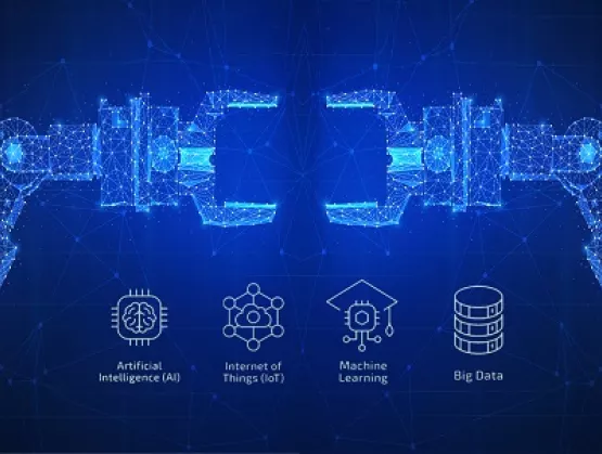
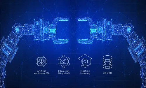
Buzzwords like digital thread, digital twin, smart manufacturing, Industry 4.0, and digital supply networks point toward a fusion of process, technology, data, and talent that promise the game-changing outcomes needed to address these challenges. Yet, there remains uncertainty about how these various elements come together into a cohesive approach across the product lifecycle. One such approach involves establishing a Model-Based Enterprise (MBE), with alignment across organizational silos, processes, and technologies. Too often, however, an effort to transform to an MBE is frustrated by “random acts of digital” that pursue implementation of certain digital technologies but fall far short of delivering value. What is needed instead is a deeper understanding of the characteristics of a true MBE and the tools and approaches to transform the organization, processes, and data to an MBE and thrive in the marketplace. Elements of a Model-Based Enterprise Modeling in engineering is not new, but what’s emerging are MBEs that comprise digital models connected upstream and downstream over the entire product lifecycle, from a product’s conception and development through its production and end market installation and use. At the heart of such MBEs are digital threads—integrated sets of processes executed within an interconnected technology ecosystem that drive the end-to-end product lifecycle and provide MBE data traceability front to back. A digital thread in the MBE environment includes all of the process, data, and system capabilities that enable digital representations of the product lifecycle stages, or digital twins, of which there are three primary types: The product digital twin is a virtual or simulated representation of the product and each of its components and configurations. While most manufacturers manage engineering models with CAD/CAE solutions, just 15% use product digital twins. Leaders in this space have seized a competitive advantage in product development and accelerated engineering. Yet, becoming a true MBE requires more than product digital twins. The process digital twin is a model of the manufacturing equipment, processes, and the workforce required to carry out related operations. The process digital twin represents the operation of the physical factory floor and its assets, complete with workflows and instructions that describe how the manufacturing processes are performed. A process digital twin relies on data from the product digital twin and allows the enterprise to build according to a product plan and predict what may happen on the factory floor. About 5% of enterprises use process digital twins. After production, a service digital twin represents the installation, use, maintenance, and repair of each product operating in the end market. The service digital twin is informed by product and process digital twins to facilitate adjustments and enhancements based on real-world data. Less than 5% of manufacturers use service digital twins, which is perhaps expected due to their reliance on the existence of the product and process digital twins. When underlying data (e.g., models, specifications, and configurations) are standardized and integrated across a digital thread, an enterprise has the capacity to monitor and refine a product over the span of the thread while also injecting insights and improvements back into the thread. The result is that engineering and manufacturing and end customer usage feedback is continuous and efficient, achieving in weeks what once took months. Visibility into materials, costs, suppliers, and more enable the enterprise to pivot and keep production moving, even when dealing with unforeseen challenges. Real-time monitoring that synthesizes live data also helps reveal performance insights and end market issues (e.g., installation issues, quality issues, etc.) that allow improvements to the offerings and operations of the enterprise. While the manufacturing and product development benefits of an MBE may be clear, the path to becoming an MBE and achieving these benefits can be challenging. Figure 1. Representative MBE end-to-end digital thread that connects product development, manufacturing, and the field (Source: Deloitte Development LLC, 2021) Accelerating Transformation New and emerging manufacturers have an opportunity to build toward their MBE vision without the historic data constraints legacy systems can impose. For more established manufacturers, such is more typical in the semiconductor equipment space, legacy technology and processes can present obstacles to an MBE transformation path. Stakeholders who have invested time and resources implementing certain enterprise platforms (e.g., CAD, PLM, ALM, MES, ERP, etc.) often look for how these can be used to enable a digital thread and digital twins over the enterprise. This limiting view frustrates a broader, more holistic opportunity to transform to an MBE and thrive in the marketplace. There is thereby a dual imperative to define a modernized and scalable end-to-end technology architecture for managing the MBE product data while also establishing a capabilities implementation roadmap that rapidly leads to MBE maturity. To be successful in your MBE transformation, four core functional capabilities that enable a digital thread must be considered: digital engineering, industrial simulation, manufacturing execution, and real-time monitoring. Addressing each with optimized tools allows a manufacturer to rapidly move from strategy to reality. Recognizing the complexity of addressing these functional needs, Deloitte has developed preconfigured solutions to help expedite and enhance transformation across each of these core areas. Design with D-PLM Simulate with D-Sim Execute with D-MES Monitor with D-IoT Accelerates product and application lifecycle management transformations with a multi-phased approach, including a phased, multi-year PLM/ALM roadmap and business case. Facilitates the ability to test and refine processes in a virtual environment, rapidly revealing the most efficient and effective industrial processes more quickly than is possible in a real-world environment. Integrates pre-defined processes related to production planning, execution, tracking and tracing, quality management, data collection, and visualization, with integrations to PLM and ERP. Delivers fast implementation of IoT capabilities that connect, collect, and analyze a broad scope of production data to drive quicker returns for high-impact areas while cultivating digital adoption. While many enterprises have various initiatives in model-based systems and manufacturing, few have tied them together with an end-to-end digital thread and set of data standards over the entire product life cycle. The foregoing preconfigured solutions can help enterprises transform to a true MBE that can typically achieve: 15% – 20% better development efficiency 30% – 50% faster time to market 8% – 20% product cost reduction 10% – 30% cost of quality reduction With such improvement potential, this could be the right time to map out and accelerate your MBE transformation to support your evolving business models and products. Deloitte Consulting LLP Co-Authors Kevin Prendeville Principal, Product Strategy Lifecycle Management [email protected] Vijay Santhanam Managing Director, Product Strategy Lifecycle Management [email protected] Kenneth Norton Senior Manager, Product Strategy Lifecycle Management [email protected] Dan Hamling Specialist Master, Technology Semiconductor [email protected] As used in this document, “Deloitte” means Deloitte Consulting LLP, a subsidiary of Deloitte LLP. Please see www.deloitte.com/us/about for a detailed description of the legal structure of Deloitte USA LLP, Deloitte LLP and their respective subsidiaries. Certain services may not be available to attest clients under the rules and regulations of public accounting. This publication contains general information only and Deloitte is not, by means of this publication, rendering accounting, business, financial, investment, legal, tax, or other professional advice or services. This publication is not a substitute for such professional advice or services, nor should it be used as a basis for any decision or action that may affect your business. Before making any decision or taking any action that may affect your business, you should consult a qualified professional advisor. Deloitte shall not be responsible for any loss sustained by any person who relies on this publication. Copyright © 2021 Deloitte Development LLC. All rights reserved.
Read More
Ride the Wave of Smarter Manufacturing The year 2020 sparked a tremendous acceleration in the digital transformation worldwide, driving a sharp rise in demand for semiconductors and escalating pressure on chip factories to reduce manual functions on the shop floor. The mindset of the semiconductor industry saw a remarkable shift as it recognized with heightened urgency the need to deploy data-driven visualization, analysis, scheduling and dispatching solutions to increase automation to improve production speed and efficiency. Amidst the new excitement around Industry 4.0, chip manufacturers are rapidly deploying new technologies including IIoT, big data, machine learning and Autonomous Intelligent Vehicles (AIVs). Yet for many chip manufacturers, the path to building a smart factory is far from clear because they lack an overall digital transformation strategy. Smart manufacturing is a broad concept covering an array of technologies and solutions, making a holistic, mid- to long-term digitalization strategy rooted in the overall business strategy crucial. There are no shortcuts that can move a manufacturer instantly to Industry 4.0. Instead, this transformation is a step-by-step undertaking with a natural evolution. Some Factory Tasks Must Remain Manual – For Now The semiconductor industry has reached a point where manual processes are no longer efficient enough to support mass chip customization and remote operations. The many technological and standardization advances behind automation can help streamline some of a factory’s most labor-intensive tasks including the loading or unloading of machines or lot tracking and data collection while reducing operational costs. Still, some tasks remain very difficult to automate. For example, handling errors and exceptions presents the greatest challenge since some errors are hard to anticipate. What’s more, the cost of automating error handling can be prohibitive. Eliminating Gaps in Connectivity Often, critical data sources aren’t available due to lack of equipment integration, incomplete product quality monitoring or gaps in material tracking. Closing these gaps in connectivity enables the collection of data and provides rich, reliable information for analysis and reporting that can drive continuous operational improvements, optimizations and efficiencies throughout a factory. But keep in mind that data integration alone can be a challenging task. The selection and proper enrichment of relevant data is, in many cases, not just a technical problem but requires a detailed and in-depth knowledge of the manufacturing steps to be analyzed and optimized. Even when data is available, it might be still difficult to make decisions or implement improvements if it is in siloed systems that require manual processes to integrate and translate into useful information. Problem solving at this level is possible but extremely time-consuming. Manual integration is not only ineffective but costly, draining time, human resources and money from the factory. The right contextual information for the data is vital to unleash its potential and make improvements possible. Dispersed solutions cannot control processes because they span functional areas and people, physical and business entities. Backbone software for shop-floor operations that controls all other applications is central to smart manufacturing. Data-Driven Manufacturing The semiconductor industry is expert in data collection and leads many other industries in this area. The problem is often that chip companies use only a fraction of the information they collect for the analysis and insights needed to improve operational efficiency. By comprehensively integrating all distributed data into a single version of truth – in one location where it is always available – companies can make data analysis and problem solving almost frictionless. Keep in mind that data platforms and edge solutions, within the context of manufacturing, will not be adopted as part of a greenfield initiative. Building a solid automation architecture is only feasible and beneficial by deploying new technologies such as machine learning and artificial intelligence (AI). Analysis of historical data provides important context and reveals deviations such as unexpected process time, uncommon material accumulations or issues with material transport. By integrating swift control actions for new data point collected, manufacturing operations can shift from reactive problem-solving to proactive analysis and operational improvements. The tremendous increase in interest and investment in AI for manufacturing automation only became possible with the availability of low-cost sensors that generate huge volumes of data and solutions for storing and processing that at low cost. AI and other leading-edge technologies transform the tedious but critical process of extracting insights from data, making it instantaneous, streamlined and achievable for every manufacturer. The maturity of smart manufacturing hinges on the extent to which a factory is data-driven. This requires foundational investments to improve traceability, connectivity and real-time operations – and finally making sure that data helps us what to do and when to do it. Ricco WALTER is managing director of SYSTEMA Automation in Singapore.
Read More
SEMI spoke with Eyal Shekel, senior vice president of Service Strategy and Excellence at Tokyo Electron Limited, about the impact of artificial intelligence (AI) on smart manufacturing and how other fab solutions for smarter process tools are advancing semiconductor manufacturing.Eyal shared his views ahead of his presentation at the SEMI Fab Management Forum, 17 February, as part of the SEMI Technology Unites Global Summit, 15-19 February 2021, an online event. Join us to meet experts from Tokyo Electron and other key industry influencers. Registration is open. SEMI: AI technology is considered a key enabler for smart manufacturing. What are the latest trends? Shekel: The advent of advanced nodes and extreme complex 3D semiconductor geometry has lengthened time to market and increased costs in areas ranging from equipment development and large-scale metrology usage to monitoring yield inhibitors.AI is becoming a critical tool in the area of material informatics to determine suitable materials and processing techniques in order to meet the needs of future devices. Together with new materials and processes, the development and implementation of virtual metrology will enable accurate and almost absolute real-time monitoring of our customers’ device wafers at each stage of the manufacturing process.SEMI: What are the benefits of data analysis in the process from R D and Ramp-Up to High-Volume Manufacturing? Shekel: The new research field of materials informatics enabled by AI provides tools to guide the highly efficient discovery and optimization of production processes. For example, TEL has developed methodologies for co-optimizing processes and materials for etch rates.To monitor and manage the yield of semiconductor fabrication processes, direct metrology measurements are important. However, it is difficult to monitor all production wafers due to the time and cost involved. With deep learning AI, it is now becoming possible to predict every wafer’s metrology measurements based on production equipment data and previously processed wafer metrology variables. This enables total quality management and run-to-run control, while simultaneously reducing production costs and cycle time.SEMI: Can you tell us more about TEL Service Advantage?Shekel: TEL Service Advantage is a TEL global support organization that allows customers to select a service plan that fits their needs. Through TEL Service Advantage, we can quickly respond to customer requests and technical advancements. TEL Service Advantage provides various plans to maximize equipment maintenance efficiency for customers and productivity from equipment manufactured by TEL. TEL Service Advantage plans can be combined to meet customer needs and achieve maximum results.A key enabling element of TEL Service Advantage is TELeMetrics™. TEL analyzes equipment data from various sensors using a remote connection and, based on that analysis, provides solutions to customer-specific problems around equipment throughput and predictive maintenance.SEMI: How is AI helping during the pandemic? Can you share a success story? Shekel: The pandemic forced severe travel restrictions worldwide, making it very difficult or even impossible in many cases to visit our customers, as it is still the case today. Standard communication devices like smartphones and email helped at the beginning when TEL intensified the remote support by our Total Support Centre (TSC).TEL continued to develop its Service Advantage program quickly, and started using additional advanced tools and methodologies such as the following: Deployed AR (Augmented Reality) to remotely assist our customer and TEL engineers Secured remote connections into TEL tools to investigate parameters and logs, or to change set-up Used remote training courses that connects trainers via video conferencing systems and training tools in the factories to skill up engineers located in a different parts of the world Used AR glasses for tool start-up and troubleshooting Expanded TEL database global technology with multi-tool on languages search capabilities A key project at a customer site in Europe offers an excellent success story. Using all the approaches above, we collaborated with the local team to put a tool into production with no major delays. This was highly appreciated by the customer and very important for us.SEMI: What do you predict for the future? Shekel: Global technology infrastructure continues to develop and expand rapidly. Elements like 5G networks, IoT and advanced sensing capabilities will lead to what we call General AI, which will be based on neuro-like infrastructure. The auto learning will spread across domains and rely on internal logic and reasoning to automate many tasks that are manual today. In our industry in particular, General AI will enable workers to focus more on data analytics and future advanced R D rather than ongoing operations.SEMI: How can technology unite us? What do you expect from your participation at SEMI Technology Unites Global Summit?Shekel: Technology united us in the last 150 years. The connectivity started with telegraph and telephone and was used to exchange information over wider distances. Nowadays, video conference capabilities, AR and improving communications technology makes it much easier to unite people who are geographically dispersed. This becomes obvious and valuable especially during this pandemic period. As a fact, we are able to continue to perform all our key activities – our tool support, training and customer relationships – even if we cannot be present in person.The SEMI Technology Unites Global Summit is a great chance to stay connected to people and customers that I would normally meet at the SEMICON exhibitions.It also offers the opportunity to network with many more people who I would not be able to meet otherwise. Moreover, I can watch speeches and presentations at any time! Normally I would miss some programs since exhibitions and events took place at the same time.Eyal Shekel, senior vice president of Service Strategy and Excellence at Tokyo Electron Europe Limited, is a 27-year semiconductor industry veteran. Upon his graduation as a Mechanical Engineer from the Technion (Israel leading technical institute), he joined Applied Materials. In 1997 he moved on to Tokyo Electron (TEL) in Europe, served as the Regional Service Manager of Israel and, soon after, was appointed the company’s General Manager. Since 2005 Eyal has been part of TEL Europe senior management. He oversaw the Service and Support Operations for TEL Europe as a senior vice president until 2019. In his current role, he co-leads TEL’s Global Service Committee in Japan.The SEMI SMART Manufacturing Initiative is a global effort to promote awareness of and interest in smart manufacturing with a focus on delivering industry-recognized best-in-class programs and services to enable members to maximize product quality and productivity while reducing costs. Activities are focused on building out core capabilities to enable smart manufacturing across the microelectronics supply chain. MADEin4 is a consortium of 47 partners from 10 countries connecting the full range of supply chain – from semiconductor equipment manufacturers and system-integrating metrology companies to RTOS and key applications such as the automotive industry. The MADEin4 Project develops next generation metrology tools, machine learning methods and applications in support of Industry 4.0 high-volume manufacturing in the semiconductor manufacturing industry. Serena Brischetto is senior manager of Marketing and Communications at SEMI Europe.
Read More
Electric mobility, renewable energy and other technology innovations like IoT, 5G, smart manufacturing and robotics all require reliability, efficiency, and compact power systems, fueling the adoption of Silicon Carbide (SiC) and Gallium Nitride (GaN) to support lower voltages in significantly smaller devices. But chip designers must overcome the technological and economical challenges of integrating the two semiconductor materials into power systems.SEMI spoke with Elisabeth Brandl, Business Development Manager at EV Group about trends and new developments within the power electronics industry and the devices' application in smart mobility. Brandl shared her views ahead of her presentation at the SEMI SMART Mobility Forum, 18 February, as part of the SEMI Technology Unites Global Summit, 15-19 February 2021, online event. Join us to meet experts from EV Group and other key industry influencers. Registration is open. SEMI: What is driving new developments in power electronics?Brandl: Globally there are significant changes in infrastructure requirements for communication, automotive and power conversion. We need to look no further than the rising adoption of 5G, electric and hybrid vehicles, and renewable energy as examples of drivers of these changes. The device level, particularly in the field of power electronics, figures prominently in these shifts.The power electronics industry faces a growing number of scenarios where conventional silicon power devices are no longer suitable and are easily outperformed by new architectures mainly based on wide bandgap semiconductor materials like Silicon Carbide (SiC) and Gallium Nitride (GaN).SEMI: What industry challenges is power electronics innovation aiming to solve? Brandl: Power conversion efficiency is very important and needs further improvement as the related losses significantly contribute to the overall power consumption. For green power and a better environmental footprint, renewable energy is crucial, but so is overall power-consumption efficiency, yet the role of power devices is often underestimated. High-frequency and high-power applications, such as data center applications and inverters for renewable energy, where silicon power electronics are reaching their limits, are also important areas in power electronics.SEMI: How will the transition from silicon to compound semiconductor materials help?Brandl: The superior material properties of several compound semiconductors can tackle the need for lower losses in power conversion or better high-frequency behavior. Today, we mainly talk about GaN and SiC power devices as they are materials well-suited to address these needs. However, other materials like diamond and gallium oxide are in development for these applications. Material properties of SiC that enable thinner materials with lower power losses and better thermal behavior address power conversion efficiency as well as form factor challenges. GaN, especially in a high electron mobility transistor (HEMT), can be used for high-frequency applications.SEMI: What enables a better and more cost-effective manufacturability of SiC and GaN power devices?Brandl: For the end customer, a typical figure of merit regarding the cost effectiveness is $ per Ampere or Watt. While this seems simple, the reality is of course more complex. It is important to understand the main cost contributors within the manufacturing area. For SiC, this is clearly the substrate cost. In my presentation, I will show a way to reduce this cost via wafer bonding. For GaN, epitaxy – a method for growing or depositing mono crystalline films on a substrate – is the critical parameter. And of course, yield has a very big impact on cost effectiveness too, which means that good process control including metrology is very important.SEMI: Many semiconductor companies are already transitioning to silicon carbide and gallium nitride. Can you give us an example of a success story?Brandl: All the big power device manufacturers have either acquired or developed their SiC and/or GaN power device technology, so they also see a bright future for these wide bandgap semiconductors in the power device market. The most prominent success story is STMicroelectronics with its SiC MOSFET power devices, which have been implemented by Tesla in its Model 3 vehicles since 2018.SEMI: What is coming next?Brandl: New materials for power devices are being explored, such as diamond and gallium oxide. For SiC, the trend is moving toward 8-inch substrates, which is the focus of the funded EU project REACTION under the coordination of STMicroelectronics. Cost reduction and substrate availability also play a big role. All major power device manufacturers have contracts to secure the supply chain for SiC substrates because material availability is the main uncertainty at this time. Finally, collaborations along the supply chain are crucial and generally beneficial for all parties, as development requirements are better communicated and prioritized.Elisabeth Brandl is Business Development Manager at EV Group. She received her master in technical physics from the Johannes Kepler University Linz, Austria in Semiconductor and Solid State Physics. Since 2014, she has been responsible for Product Marketing Management for temporary bonding and compound semiconductors at EVG. The SMART Mobility Forum is the digital platform of SEMI Europe’s Global Automotive Advisory Council (GAAC) for industry stakeholders along the automotive and electronics value chains, from Design, Semiconductor Equipment and Materials Suppliers to Automotive OEMs.Smart Mobility is one of four SEMI initiatives focused on building communities, content, and activities around critical and emerging electronics markets. Read more about our Regional Chapters.Serena Brischetto is senior manager of Marketing and Communications at SEMI Europe.
Read More
The turn of the New Year means new opportunities for the microelectronic industry as SEMI continues to focus on a top priority for companies across the microelectronics design and manufacturing supply chain and SEMI members – supporting the development of the talent pipeline. Regardless of a member company’s role within microelectronics, ensuring a continued, robust flow of qualified talent for what is a cross-cutting, foundational industry sector is of high strategic importance. Skilled workers are essential to advances in areas such as artificial intelligence (AI), smart manufacturing, medtech, transportation and communications. In order to satisfy the world’s insatiable appetite for technology, we need a qualified workforce that can design and manufacture cutting-edge microelectronic devices. Launched in 2019 by SEMI’s Government Programs Office, SEMI Works™ is a holistic approach to developing and maintaining the talent pipeline. 2020 focused on building the all-important infrastructure, engaging member companies to identify required skills and developing a Unified Competency Model to catalog these workforce requirements. SEMI Works™ accomplished several firsts for the microelectronics industry: First dynamic, data informed workforce training standard adopted and published by the U.S. Department of Labor Employment Training Administration (USDOL-ETA) First SEMI Certified college program for technicians First Industry Approved Apprenticeship Program for Technicians, adopted and endorsed by the U.S. Department of Labor Member inputs anchor the SEMI Works™ portal, which enables connections among talent, employers and training/education providers. The portal’s initial phase of development is on track for completion in the first quarter of this year, marking the point when it will begin to be populated with specific job information, individual (talent) profiles and applicable training courses. Once SEMI Works™ is fully operational, it will be optimized to further support talent development and acquisition, providing a comprehensive platform for learning management, e-learning and career advancement. Throughout 2021 SEMI will be engaging members, training providers and job seekers to ensure the portal’s capabilities and user interface meets their needs. We’ll also move forward with several other SEMI Work’s programs including the Curated Content Initiative, which will enable SEMI members to identify non-proprietary courses, a SEMI member job board and an interactive career map to help job seekers plan their future in the industry. The microelectronics industry will only fulfill its tremendous promise for innovation and growth with the right talent. SEMI looks forward to working with members in 2021 to expand SEMI Works™ and help lay the groundwork for the next wave of technology advances. Mike Russo is vice president of Industry Advancement and Government Programs at SEMI.
Read More
Nexperia became a standalone company about four years ago after our divestiture from NXP Semiconductors. Last year we started our journey towards smart manufacturing at our back-end factories in Asia by developing a roadmap to help steer us in the right direction.Our first step to creating a convincing and workable smart manufacturing roadmap was to define the very meaning of smart manufacturing to Nexperia. Since the definition of smart manufacturing varies widely, we started by looking at two different and distinct technology adaptations: Physical automation Data-driven manufacturing, or using analytics at the core to develop and adopt machine learning and artificial intelligence (AI) models It is important to find the right balance of investments between physical automation and data-driven manufacturing to steer clear of deployment inefficiencies since only connected solutions deliver full value. Our approach involved the following high-level steps. Meeting with internal management teams for their inputs and examining factory needs and maturity Meeting with other semiconductor factory operators, subcontractors and partners to review their smart manufacturing approaches and challenges Evaluating our needs and status against the Singapore Smart Industry Readiness Index model Physical AutomationEvaluating the maturity of available solutions and adaptions by the industry and our own shop floor helped simplify the thought process quite well. Logistic automation is not new. Very mature solutions, even for custom layouts and preferences, are readily available. Shop floor automation is far more difficult than logistic automation since variability is simply too high. Traditional shop floor investments were always driven from quality or OEE perspectives and not necessarily very well connected. Our approach is outside-in – deploy logistic automation first and then move to the shop floor.Data-Driven ManufacturingHow smart manufacturing becomes depends on the extent to which a factory is data-driven. Enabling data-driven manufacturing requires foundational investments to improve traceability, connectivity and real-time operations. We believe real-time awareness can drive machine-level and closed-loop process control critical for predictive, cognitive control of the shop floor.Real-Time Awareness and Traceability is at the CoreDeveloping real-time awareness requires wide-ranging manufacturing protocols. The following focus areas have helped us simplify the challenge: Connectivity Core systems for areas including MES, quality and SAP Analytics and AI Digital shop floor featuring one operator interface with real-time control systems Readiness of engineers, technicians and managers Each of these pillars has different level of complexity due to legacy equipment and systems, legacy processes and inexperience of engineers with automation. This makes deployment of data-driven operations a complex challenge. We looked at different project approaches for each of the focus areas: Core Systems – Build additional technology enablers and roll them out with prioritization planning. Analytics – Focus mainly on OEE and yield with automated root cause analysis and predictive approaches. Real-Time Control – Merge the initiative with factory-level programs to improve productivity and quality. With a strong smart manufacturing roadmap, the next challenge is to secure long-term buy-in on the plan and required investments from executive management. Visiting and otherwise connecting with peer sites that have already deployed smart manufacturing infrastructure is vital in this effort. Thanks to SEMI members, we were allowed to visit their factories with our management team for go-and-see tours since seeing is believing in the smart manufacturing journey. Our executives also met with subcontractors and vendors to better understand the value of this transformational undertaking.A long-term outlook is necessary to successfully develop a smart manufacturing roadmap, and executive commitment goes a long way to ensuring its success. We are excited about our smart manufacturing journey and believe it is a game changer for our factories.Adarsha MARPALLI is director of Factory Automation at Nexperia B.V.
Read More
While Artificial Intelligence (AI) emerged in the 1950s, only in recent years have AI applications proliferated with the explosion of data and continuing improvements in Moore’s law that have driven rising processing speeds. Voice assistants, image analysis software, search engines, and speech and facial recognition systems were among the first applications to use AI. Today, adoption has spread to sectors such as agriculture, cybersecurity, healthcare, software development, e-government and the intelligent enterprise to generate jobs and help spur economic growth. The Edge AI Opportunity and the Microelectronics IndustryAI can be embedded in hardware devices such as advanced robots, autonomous cars, drones or Internet of Things (IoT) applications. Today, according to the EU’s digital strategy, data centres and other centralized computing facilities account for the vast majority – 80% – of AI data processing and analysis, with smart connected objects such as automobiles, home appliances and manufacturing robots that bring the compute function closer to the user representing 20%. The latter, known as Edge AI applications, are powered by edge-based machine learning chipsets, not the AI chipsets designed to run cloud-based machine learning algorithms.The EU’s white paper on AI published in February 2020 anticipates that the way data are stored and processed for AI applications will change significantly over the coming five years as edge computing applications proliferate. Most AI applications need to connect with devices that collect data and manage data flows. When the applications connect with cloud infrastructures to train large volumes of data for a machine learning model, the interface devices often require hardware support. Edge AI can minimize data transport by processing data directly from local devices to accelerate data analysis and decision-making and make data transport or accelerator hardware unnecessary, critical in reducing power consumption and enhancing data security for applications such as autonomous driving. Over the past 40 years, the ICT sector has been continuously increasing greenhouse gas (GHG) emissions despite efforts to shift to renewable energy. Cloud-based AI applications require an ICT infrastructure for high-performance computing and high-speed connectivity. According to MIT Technology Review, data centres’ AI workloads could account for a tenth of the world’s electricity usage by 2025. a mass update of cloud-based AI applications may significantly increase energy consumption, unlike with Edge AI. This is why the strategy for developing Edge AI is well-aligned with the EU’s Green Deal objectives. Europe aspires to play a leadership role in Edge AI to strengthen the sector’s competitiveness and protect the European digital sovereignty. Europe’s strong industrial competencies in embedded systems and microcontrollers will help the region promote development of European domestic AI solutions for emerging high-value IoT applications in industrial processes such as Industry 4.0, Connected and Automated driving (CSA), smart cities, climate action, healthcare, and national defence and security. With this strong strategic position in technology, Europe is well-positioned to invest to become the leader in the Edge AI global market.Preparing the Workforce for the Microelectronics IndustryTo design and manufacture leading Edge AI chipsets, European education providers and industry will need to work closely together to train the current and future workforces. Within the framework of the METIS project, a four-year project co-funded by the European Commission through the Erasmus+ programme, SEMI and imec deployed experts in the field to survey and interview focus groups. The survey identified the following key focus areas for workforce development: 1. True Capability of AI and Data Science With AI’s heavy dependence on data, the workforce of the future must be trained in areas of data science including data integrity to ensure quality, unbiased sourcing, collection and accurate analysis necessary to interpret huge volumes of data. Europe also needs to train the next generation of AI chip designers in data security and privacy – key challenges to the widespread deployment of Edge AI chips. 2. Climate Change, Sustainable Development Goals (SDGs) and Social Inclusion TrainingSince the industry must be able to develop Edge AI solutions to enable the digital transformation while limiting GHG emissions, microelectronics engineers need to be schooled in climate change and understand how their work contributes to meeting the United Nation’s Sustainable Development Goals (SDGs). Workplace diversity and social inclusion are also important target areas for education since Edge AI applications should serve various groups of people with different needs.3. EthicsChip industry workers must also be educated in ethical issues of AI related to the technology’s potential societal impact in the near future[1]. With AI applications capable of monitoring Internet searches based on users’ personal preferences and biases to deliver tailored advertising, news and other information, developers must recognize how the technology can influence thinking and behaviour of individuals and groups. This awareness can help developers strike a balance between supporting commercial interests and societal good so the microelectronics industry can ensure ethical implementation of AI. 4. Cross-disciplinary Skills Required for AIAI development requires a comprehensive, cross-disciplinary skill-set to be able to integrate the work of specialists from diverse educational, cultural and professional backgrounds critical to developing non-biased AI solutions. For example, in addition to technical expertise, microelectronics AI developers must be able to communicate clearly and work in close-knit teams with non-technical experts from business, law, medicine and the social sciences.What’s Next?The microelectronics industry has a tremendous opportunity to develop new chip-based solutions for AI architectures, and apply AI techniques to improve operational efficiencies of design and manufacturing. To seize this opportunity, the industry must work closely with education providers to groom the next generation of skilled workers. This tight collaboration is critical to designing and delivering specialised courses to college and university students as well as engineers now working in the chip sector. The stakes are high. By preparing workers to develop Edge AI chipsets, the microelectronics industry can help the world confront some of the greatest challenges it faces today.For more information, see SEMI Responds to European Commission White Paper on Artificial Intelligence.METIS is a Sector Skills Alliance project co-funded by the European Commission’s Erasmus+ Program and coordinated by SEMI. The four year project, launched in November 2019, will develop a Microelectronics Skills Strategy. Based on the strategy, the METIS project will design 43 training modules for 1,100 hours learning in four key areas of the microelectronics sector.We thank Patrick Blouet (STMicroelectronics) and Jeroen Geusens (imec) for their valuable contributions to this article.[1] Ethics of Artificial Intelligence and Robotics, Stanford Encyclopedia of PhilosophyDr. Yanying Li is senior manager of Collaborative Projects at SEMI Europe.Dr. Pushkar P. Apte is the strategic technology advisor for the Smart Data AI Initiative at SEMI
Read More
D-SIMLAB Technologies, a Singapore-based provider of simulation-based business analytics and optimisation software solutions, recently joined SEMI. I spoke with Peter Lendermann, the company’s co-founder and Chief Business Development Officer, about the company’s role in the smart manufacturing movement, how customers are benefiting from D-SIMLAB solutions, and what the future holds for smart manufacturing. Ng: What is D-SIMLAB’s mission?Lendermann: Our mission is to develop, market, and deliver high-performance simulation-based decision support solutions that enable corporations to enhance their performance in a sustainable manner leading to significant cost savings. In particular, we focus on semiconductor manufacturing material flow planning and optimisation but also do business in aviation where we help customers optimise their spare parts support operations. What these two domains have in common are three important attributes: They are capital intensive, their underlying operations are complex, and operations are also heavily affected by random, i.e. unpredictable events, which makes both planning and execution of manufacturing operations very challenging. D-SIMLAB is a spin-off from the Singapore Institute of Manufacturing Technology (SIMTech) under the Agency for Science Technology and Research (A*STAR). Our head office is in Silicon Island Singapore. We also have representations in Germany and the U.S. Most of our staff are industrial and computer engineers with up to 20 years of operations experience in their respective industry domain, as well as vast data analytics and software development capability.Ng: What solutions does D-SIMLAB offer to optimise semiconductor manufacturing?Lendermann: In the three-pillar smart manufacturing framework of Connect, Sense and Predict advocated by SEMI, our focus is on Predict though we emphasise the equal importance of the subsequent Act: Our solutions can Predict, for example, WIP waves or usage-based preventive maintenance due dates. But much more value-add can be realised once some decisions with regard to how to Act can be derived from such a prediction. The ability to pro-actively adjust action plans in a timely manner is essential to overcoming challenges arising from changing customer due dates, mix profile changes, untimely production line issues, and production capacity to be shared with R D lots effectively, so that ultimately our customers can enhance capacity, reduce cycle times and improve the due-date performance of their factories.To that end, our D-SIMCON solution suite spans the full spectrum of decision-support tools required to forecast, manage and optimise material flow – from operational scheduling and dispatching, WIP forecasting and dynamic and static capacity planning all the way to specific applications for fab load mix optimisation or for the enhancement of the product/layer dedication and resist allocation in the lithography area. Our solutions are implemented in numerous 6-, 8- and 12-inch wafer fabs operated by both IDMs and foundries worldwide with capacity ranging from 40,000 to 200,000 wafers per month.Ng: What are the key enablers of D-SIMLAB’s success?Lendermann: Our success lies in deploying production-ready solutions for our customers, allowing them to extract immediate value. Our solutions enable the portrayal of many domain-specific characteristics such as queue time constraints or specific equipment behaviour, which is absolutely essential to generating operationally feasible plans or schedules in order to be able to Act in the best possible manner according to what has been Predicted. Moreover, we have modules for automatic generation, calibration and maintenance of the underlying capacity model, including resolution of data inconsistencies as well as verification and validation of the model, to allow near real-time responses to continuously changing operations. And the associated optimisation approaches focus on creating maximum possible value with as few iterations as possible and within minimum time through smart heuristics and parallel computing infrastructure – a paradigm that is as powerful as it is cost-effective.Ng: What are a few of your more notable customer successes?Lendermann: As a result of the first implementation of our novel, multi-objective based Scheduler cum Dispatcher, a tool capacity gain of 8%, a transportation capacity gain of 10%, and an operator workload reduction of 25% were concurrently realised at one of the critical equipment groups in our customer’s fab. At another set of equipment groups in the same fab, a 7% increase of lots within the critical queue time limiting area was achieved.Another use case we successfully realised is fine-tuning of Preventive Maintenance plans: Based on a seven-day lot arrival forecast at each equipment generated with our WIP Forecaster, a recommendation is made when PM would be best possible without causing too much disruption in the WIP flow. The effect of this synchronisation of the PM plan with material flow enabled a dramatic reduction of the average queue lengths at critical equipment groups and the associated cycle times without incurring any capacity loss. Reduction of average queue length as a result of synchronising preventive maintenance with material flow. Ng: What challenges has D-SIMLAB been facing in the COVID-19 world?Lendermann: Obviously, software delivery projects have become more challenging for the time being since our engineers cannot be on-site frequently. But it also turned out that more and more services can be delivered remotely, which has the nice side effect of making the services more cost-effective for customers. Overall, we are confident that our solid customer base will enable us to sail steadily through these challenging times.Ng: Where does D-SIMLAB see the technological development heading?Lendermann: In the future, enriching decision support and manufacturing execution solutions with machine learning and other AI techniques will be critical in reducing dependency on human experience. This path is essential to making manufacturing operations fully Industry 4.0-compliant. D-SIMLAB will certainly be at the forefront of this development. Bee Bee Ng is president of SEMI Southeast Asia.
Read More
Not long after STMicroelectronics opened its first semiconductor plant in Singapore more than 50 years ago, a facility chiefly focused on chip assembly and packaging, the company realized that it had constructed the site in an area with a blossoming chip ecosystem with a bright future. Before long, the company became the first to start a wafer fab facility in the so-called Little Red Dot. Today, our STMicroelectronics Singapore campus sports several buildings that dwarf the original site in the sprawling Ang Mo Kio Industrial Park 2. The facilities feature advanced 200mm manufacturing lines but still produce huge volumes of chips with more than 1,000 pieces of 150mm manufacturing equipment.Much of the wafer equipment dates back to the past century so is no longer supported by the manufacturers, if they’re still even in existence. Yet decades later the chipmaking gear continues to operate with a surprising reliability that far surpasses the longevity called for in its manufacturing specifications thanks to replacement parts and frequent upgrades with more sophisticated handling robots and chucks. Now, as smart manufacturing begins to establish a foothold in the semiconductor industry, Industry 4.0 technology is breathing new life into these aging workhorses.Despite its age, all of the equipment adheres to industry manufacturing standards. The gear is remotely controlled using the SECS/GEM interface protocol that was either originally integrated with the equipment controller or custom-made. We’ve also maximized its usage through advanced recipe management, advanced alarm and event handling, and secured lot identification.Crucially, we decided to systematically deploy a real-time fault detection and classification (FDC) solution using a third-party product based on what today is known as an edge computing architecture. Every piece of critical processing equipment is progressively paired with its dedicated FDC instance running on a virtual machine in the wafer fab data center, and the FDC solution monitors vital equipment parameters at high frequency – depending on the SECS/GEM capabilities of the equipment – and analyzes incoming manufacturing data in real time using classic SPC (statistical process control) algorithms and even AI-class protocols.Our use of the FDC edge solution as a sensor signal aggregator has given our equipment a second life. The solution processes real-time signals from sensors connected through a typical TCP-IP. Sensors have been the old equipment’s saving grace with their ability to de-multiply equipment capabilities and overcome fundamental shortcomings and design weaknesses. The STMicroelectronics Singapore plant first used off-the-shelf sensor nodes with built-in power amplifier and analog input nodes. While very practical and easy to implement, deploying the nodes can be costly. After developing more expertise in sensor integration using FDC, our wafer fab equipment experts decided to design an in-house solution based on the famed STM32 microcontroller. Leveraging Arduino – an open-source electronics platform with easy-to-use hardware and software – the equipment teams can now design and program a variety of in-house sensors for measurements including temperature, humidity, waterflow and pressure. The sensors are integrated with process equipment using the FDC solution. Integrating the sensors with the FDC engine on the edge computer extends the capabilities of old equipment without jeopardizing the integrity of the machines themselves. While the integration can be quick, it must be robust to ensure the reliability of the new measurements. Similarly, ever-increasing connectivity requirements present clear cybersecurity risks that must be managed upfront and each solution must be hardened to minimize security vulnerabilities. Even so, the challenges and risks pale in comparison to the benefits! Jean-Marc PHILIPPE is DIT Director at STMicroelectronics Pte Ltd. He oversees the deployment and support of Digital Solutions to enable STMicroelectronics front-end operations in Singapore and manages manufacturing productivity and automation programs at site level.
Read More
SEMI is pleased to welcome Singapore-based UTAC Holdings Ltd., formed nearly 50 years ago, as a new member. UTAC is a leading independent provider of assembly and test services for a broad range of semiconductor chips, offering a full range of semiconductor assembly and test services across analog, mixed-signal and logic, and memory. Its customers are primarily fabless companies, integrated device manufacturers and wafer foundries. The company has production facilities in Singapore, Thailand, China, Indonesia and Malaysia as well as sales offices in five regions: the United States, Japan, China, Taiwan, the rest of Asia and Europe.I recently spoke with Dr. Nathapong Suthiwongsunthorn, Vice President and General Manager of UTAC Thailand, about UTAC’s smart manufacturing advances, the company’s role in the semiconductor industry’s transformation, and the industry outlook for Thailand over the next year.Ng: How does UTAC Thailand complement your other facilities?Dr. Nathapong: As one of the world’s largest producers of quad-flat-no-leads (QFN), UTAC Thailand has significant capability in assembly and test of advanced leadframe products including power products such as Cu Clip packages as well as MEMS products. We also serve top global IDMs and have the largest share of assembly and test for the automotive market among all UTAC operations. UTAC’s other facilities have expertise in wafer-level packages and system-in-a-package and serves the communication and consumer market not only for IDMs but also for the fabless and foundry companies. The Thailand factory nicely complements the other UTAC facilities both from the standpoint of operational and marketing diversity. Ng: UTAC Holdings Ltd. announced in August this year that it has completed its sale to Wise Road Capital, a global private equity firm. Will this in any way change the operation and business strategy of UTAC Thailand?Dr. Nathapong: I don’t believe it will change the way we operate. However, the acquisition is very positive for us from a financial perspective. With the benefit of significantly reduced debt and interest expenses, we will be able to expand our business to grow with and hopefully beyond the semiconductor market. Ng: To what extent has UTAC adopted smart manufacturing?Dr. Nathapong: UTAC Thailand is leading the way in terms of automation, smart manufacturing and Industry 4.0 with our in-house automation team and unique expertise. For example, we have built our own inspection equipment that is much faster and cheaper than what is commercially available. We also working on many programs such as mobile robot, AGV, auto inspection and office automation to help drive greater production efficiency. We are replicating our manufacturing advances and fanning them out to other UTAC facilities.UTAC Thailand Ng: What are some of the challenges you face in pushing for the industrial transformation in Thailand?Dr. Nathapong: I think the key challenge is to find skilled engineers who can perform hardware- and software-related tasks critical to the industrial transformation. But frankly, we have done a good job in managing this challenge by hiring very smart people, providing them with the required in-house training, and using outside training for new recruits as necessary. We have developed partnerships with capable vendors in this regard as well.Ng: What are the key differentiating elements (e.g. talent, tax, technology, trade, EHS) in Thailand that have been instrumental in supporting the E E ecosystem?Dr. Nathapong: There are two key differentiating elements for us. Firstly, UTAC has been around for over 47 years and is very well-established in Thailand with a positive reputation as an employer. This makes hiring talented people relatively easy. Secondly, and perhaps more importantly, the nature of the Thai people and also the benefits the company provides make it relatively painless to retain key employees. I also believe that we have a significant number of engineers available in Thailand. Finally, labour costs in Thailand are still very reasonable and stable. So we are able to acquire talent at a very competitive rate compared to other countries. Ng: What is the industry outlook for E E industry in Thailand over the next year?Dr. Nathapong: Surprisingly, the current sad predicament of COVID-19 has shown no negative impact for the global semiconductor industry – people seem to be buying more electronics with the lockdown. Our outlook for the Thailand’s E E industry is similarly very positive. Most semiconductor companies including UTAC see significant growth this year and I hope it will continue.Ng: With the recent semiconductor geopolitical and trade tensions, are more customers moving their business to Thailand?Dr. Nathapong: I believe so. We do see some of our key customers move manufacturing out of China and into Thailand. The relocations help them offset or avoid any potential fallout from current geopolitical tensions.Ng: In what areas do you think SEMI Southeast Asia can play a role to help our members companies in Thailand like UTAC?Dr. Nathapong: The semiconductor industry has been in Thailand for a long time. In fact, UTAC Thailand is 47 years old this year! However, I feel that Thailand never really worked with a strong establishment organization like SEMI that can connect various companies together to help drive innovation. I think SEMI Southeast Asia can truly help Thailand to move up to the next level of providing semiconductor solutions globally. We welcome SEMI Southeast Asia’s help in this regard.About Dr. Nathapong SuthiwongsunthornDr. Nathapong Suthiwongsunthorn joined UTAC in 2009 and is currently General Manager of UTAC Thailand, UTAC’s largest operation site. Before taking over the management of Thailand operations, he was Vice President of Research and Development, running UTAC’s global R D group. Dr. Nathapong has more than 20 years of experience in the semiconductor industry. He holds more than 40 international patents and publications in wafer-level and advanced packaging.Prior to joining UTAC, Dr. Nathapong held several key leadership positions in research and development at Schott, STATS ChipPAC and Infineon. Dr. Nathapong has a Ph.D. in Electronics Engineering from Oxford Brookes University, England.Bee Bee Ng is president of SEMI Southeast Asia.
Read More