downloadGroupGroupnoun_press release_995423_000000 copyGroupnoun_Feed_96767_000000Group 19noun_pictures_1817522_000000Member company iconResource item iconStore item iconGroup 19Group 19noun_Photo_2085192_000000 Copynoun_presentation_2096081_000000Group 19Group Copy 7noun_webinar_692730_000000Path
Skip to main content
Default Banner Image

semiconductors

The march of innovation in semiconductor microfabrication technology over the past 60 years has produced electronic devices and information systems that have transformed industries and lives around the world. And while advances in chip technology continue to make it possible to collect, transmit, store and process more data for a rapidly growing universe of applications, the pace of innovation is now facing strong headwinds. Powered by chip innovation, data centers have become massive centers of information processing but, on the downside, enormous consumers of electricity. Today, the power-hungry hubs account for five percent of the world's electricity usage, a proportion that is growing every year, raising important questions about sustainability. Compounding the challenge, the pace of Moore's Law, for decades the engine of electronic device and information system innovation, has slowed. While the research and development of state-of-the-art semiconductor fine processing technology remains robust, developing the advanced manufacturing technology for mass-producing more sophisticated electronics devices is becoming harder, as is ensuring business profitability."It has become difficult for semiconductor technology to continue to evolve as it has in the past," said Akira Minamikawa, Research Director of Technology Research at IHS Markit, who moderated the Semiconductor Executive Forum – View by Top Two in the Era of Digitalization on opening day of SEMICON Japan 2019 at Tokyo Big Sight. Held at the SuperTHEATER, the forum featured Terushi Shimizu, representative director and president at Sony Semiconductor Solutions, and Atsuyoshi Koike, president at Western Digital Japan, two industry powerhouses that could figure heavily in the future of digital technology. SuperTHEATER, the main stage at SEMICON Japan 2019 Image sensors evolve to become eyes of AIImage sensors are becoming eyes of artificial intelligence (AI) and intelligent systems that monitor people and events worldwide, collecting data that one day could help puzzle out growing social challenges such as energy conservation and traffic congestion. With 51 percent market share on the strength of its industry-leading technology, Sony Semiconductor Solutions dominates the image sensor market. Despite last year’s global semiconductor industry slump, the company’s “business continues to enjoy strong growth and we are very busy,” said Shimizu, who attributed the company’s robust performance to the rising importance of the social role of image sensors and the expanding number of applications they support.The success of the company’s image sensors can also be traced to its division of the image sensor market into two application categories: "Imaging" focuses on capturing beautiful image data, while "sensing" aims to collect data that accurately describes the state of a subject and its surroundings."In 2019, sales of imaging products for smartphones grew rapidly,” Shimizu said in his market overview. “This is due to the average annual 15 percent growth rate of multi-camera smartphones, with some phones today featuring seven cameras, and an average annual growth rate of 20 percent in sensor size to produce higher image quality."But Shimizu cautioned that Sony Semiconductor Solutions doesn’t expect the smartphone sensor market to maintain that fast growth rate."The imaging market is expected to grow until 2022, but after that, the sensing market will drive market growth,” he said, adding that the company’s “capital investment plan is based on this scenario."AI will be key in catalyzing growth of the sensor market as integrations of AI processing engines and sensing images grow in sophistication to capture images undetectable by the human eye, Shimizu said. AI will extract insight from captured image data. For its part, Sony will apply its layer stacking technology to sensing products."By stacking an AI processing engine, we want a significant portion of the recognition processing done within the sensor chip," Shimizu said.One sensor the company already offers collects in-depth information for indirect time-of-flight (ITOF) 3D ranging for new user interfaces relying on autonomous or gesture control for robotics. The sensor “was first used in smartphones in 2018 and saw widespread adoption in 2019," Shimizu said.Sony Semiconductor Solutions plans to focus on developing new sensors for integration with their ultrasonic cousins. Aided by optical deflection technology, the sensors will be used for product quality inspections during manufacturing.With the company’s growing strengths in sensor technology, it hopes “to increase sales of sensors from a few percent of the company’s total sales in 2018 to 30 percent in 2025,” Shimizu said, pointing to its goal "to capture 60 percent share of the image sensor market by 2025."Data as one way to spread happinessAt the heart of consumer devices such as smartphones and computers and also cloud servers, NAND flash has made it possible to process vast troves of data anytime, anywhere. In recent years, the technology has enjoyed stronger adoption for use as the storage medium of choice for edge computing, stationed between end devices and the cloud to help streamline data utilization. But the technology isn’t merely about making smarter use of bits and bytes."We would like to promote the technology development that can support the use of data to bring happiness to people around the world," Koike of Western Digital Japan said. The company calls data that contributes to individual happiness and helps solve social issues "data for good" and, like the Sony Semiconductor Solutions bifurcated classification of the image sensor market, categorizes information into “big data” and “fast data.”For example, big data can leverage AI to drive dramatic improvements in the interpretation of test data and, ultimately, the diagnostic accuracy of mammography for breast cancer screening, aiding in early detection to help save lives, Koike said. Fast data can be harnessed to analyze data collected from a manufacturing equipment line in real time to improve production efficiency. The company’s plant in Yokkaichi, Mie Prefecture, which the company operates in cooperation with Japanese memory manufacturer Kioxia, already uses fast data to bolster production.More NAND flash innovation and greater supply capacity are critical to developing "data for good," Koike said. "It is difficult to expand clean rooms at the same pace as data usage grows. In order to continue to advance technology and enhance supply capacity, we need to adopt new ideas for building production lines. We need a smaller equipment footprint, shorter cycle time and higher throughput."Semiconductor market shows signs of recoveryIn their discussion of the short-term outlook for the semiconductor market, Shimizu and Koike pointed to the importance of strengthening the talent pool of Japan’s semiconductor industry as global competition heats up with China’s pursuit of semiconductor independence and the industry pulls out of the 2019 slowdown fueled by weak memory prices. While Sony’s business has been buoyed by strong image sensor demand for smartphones, the devices “did very well, but other applications didn't," Shimizu said. Even the image sensor market stagnated.Despite the 2019 slump, market conditions and capital investments by semiconductor manufacturers have been on the upswing."In the second half of 2019, the Chinese market showed signs of recovery triggered by 5G,” Shimizu said. “In 2020, this movement is going to be in full swing around the world and we will be busier than last year."Koike agreed: "The semiconductor market for data centers will recover with 5G. The hard disk shortage is already an indication of a recovery, a turnaround that will undoubtedly extend to solid state drives (SSDs). In addition, advances in autonomous driving technology will ensure continued growth of the automotive semiconductor industry.”Japan should embrace international competition, not fear China's pursuit of chip independenceIt's no secret that China is investing heavily in its semiconductor development capabilities to move up the microprocessor value chain. Minamikawa posed the question: How should Japanese chip companies navigate the shifting regional balance of power? "It is natural for China to strive to establish domestic procurement of semiconductors that are fundamental technologies for various industries,” Koike said, “I think the efforts of Chinese companies are outstanding in that they are not pursuing short-term results, such as improving yields in the near future, but are making efforts with an eye to achieving results in 10 years. Japan has a variety of options including working with China to create joint ventures and competing head-on. Regardless of which choice we make, however, it is imperative for the survival of domestic companies that Japan maintains its technological competitiveness to remain ahead of China."Shimizu said that Sony’s “Chinese customers are quick to take action and study extremely hard. We often have opportunities to share our roadmap with them and explore innovation opportunities together. Before, they were passive and relied on us for insights into new technologies, but now they are more assertive and I sense that they will start to drive innovation.”Koike added that "although Japanese companies often talk about business globalization, neither Chinese nor American companies say much about it. While global expansion is a major requirement for business, I think Japanese companies need to focus more on the Japanese market overall, not just when they think about the growing competitiveness of Chinese companies." L-R: Akira Minamikawa, Research Director of Technology Research at IHS Markit; Atsuyoshi Koike, president at Western Digital Japan; Terushi Shimizu, representative director and president at Sony Semiconductor Solutions Talent key to bolstering competitiveness of Japan’s semiconductor industryMinamikawa of IHS Markit didn’t mince words in describing the talent shortage in the Japanese semiconductor industry as “grave,” saying that “the workforce challenge is not endemic to the electronics industry as evidence grows that the number of people obtaining doctorates in Japan is falling and the educational level of the Japanese population as a whole is in decline.”Three years ago, Shimizu interviewed professors on Kyushu island for insights into Japan’s talent shortfall. He came away feeling that “Japanese semiconductor companies were not sufficiently communicating the industry's talent and innovation needs to professors. To help professors and students better grasp the appeal and potential of the industry, we have started to send frontline engineers to universities to educate students and instructors about their work and careers. Expecting corporate HR departments to alone solve the talent shortage won’t work.”"In Japan, if you advance to a doctoral course, you will have a hard time getting a job, which is a strange situation,” Koike said. “Companies and universities need to work together more closely to better understand how to attract and hire doctoral graduates."Minamikawa said companies must have strong leaders with clear missions to attract the right talent, but Koike pointed to the drawbacks: "The image of a company with a strong leader seems to be cool, but it also has a downside because engineers stop thinking for themselves and wait for instructions from the top. I believe it is important for company leaders to have ongoing discussions at all organizational levels and lead the way in times of confusion."Shimizu agreed, citing his own company as an example."Thankfully, our company is very busy right now,” he said. “However, some employees are starting to request more time to think about how to improve the quality of their work. To maintain and strengthen our competitiveness and continue business growth, I believe it is important to cultivate an environment that encourages each employee to take more time to think for themselves."Motoaki Ito is the CEO of Enlight, Inc. and a reporter for SEMI. Mayumi Amagai is a marketing manager at SEMI Japan.
Read More
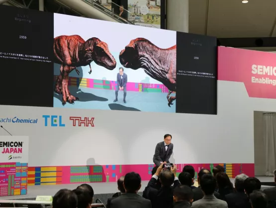
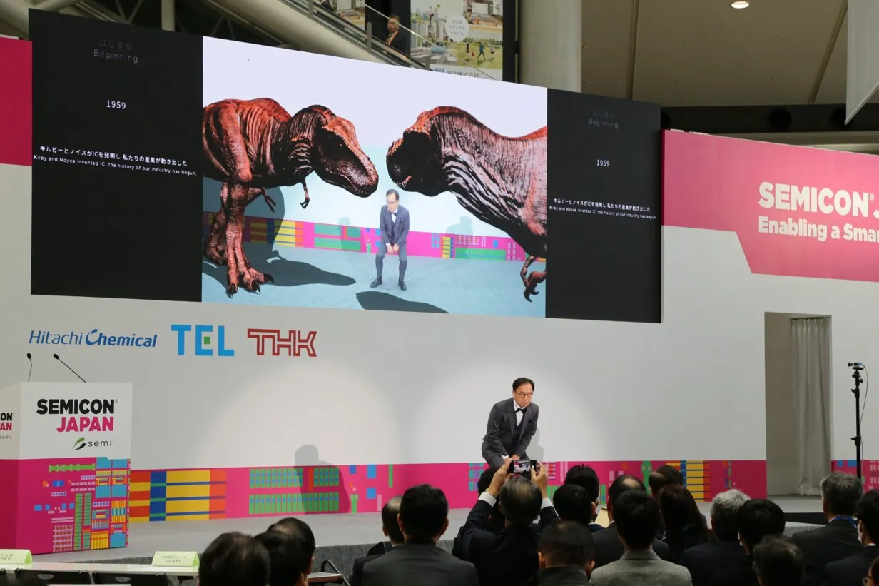
Augmented reality (AR) tyrannosauruses towered on-screen as I interacted with the creatures in a mix of prehistoric and cutting edge. Or, rather, my AR double was doing the playacting. Minutes later, virtual doppelgangers of a small lineup of chip industry executives cut the ceremonial ribbon. Seemingly sweeping away the winter chill, the opening of SEMICON Japan 2019 dazzled with smart technology and the promise of lives, cities and workplaces transformed, with uber-intelligent applications in full display at Tokyo Big Sight. But what resources does the industry need to harness to drive the next era of innovation? The semiconductor industry’s unwavering passion and young talent are key, said Hiroshi Imano, Chairperson of the SEMICON Japan Initiatives Committee, in his opening keynote. And hardly any region of the world is in a better position to help realize that future than Japan, Imano said. The region supplies one third of the equipment and more than half of all materials to the global semiconductor manufacturing industry.Talent was also top of mind for SEMICON Japan 2019 keynote speaker Makiko Eda, Japan's Chief Representative Officer at the World Economic Forum (WEF). Serving as a platform for public-private partnerships, the organization's mandate is to tackle global issues such as climate change and geopolitical strife in making world more resilient to risk and, by extension, more sustainable.Spanning ecology, economy, technology, society, geopolitics and industry, that mission includes reskilling and upskilling a billion people over the next decade, a high priority for WEF, which hosts a conference every January in Davos, Switzerland. The theme of this month's conference – Stakeholders for a Cohesive and Sustainable World – reflects the vital importance of building the international partnerships and global consensus necessary to achieving WEF's goals.One key to that sustainability will be technology and Arm, a global chip design company, will play a key role, with the company’s chips touching over 70 percent of the world’s population, Arm president Yuzuru Utsumi said in his keynote. Today, Arm is driving toward an ambitious goal: Ship 100 billion chips from 2017 to 2021 – the same number produced over the previous quarter century – by powering advances in mobile computing, server and networking infrastructures, and automotive applications.Arm’s innovation ecosystem of more than 1,000 partners will deliver these chips as they continue to work together to develop differentiated technology. Arm plans to increase investments not only in its primary processor business to accelerate market share gains but in the company’s new IoT business to create new revenue streams. The goal: Deliver long-term sustainable growth, Utsumi said. SEMICON Japan 2019 showcases SMART manufacturing and transportation Billed as a showcase of smart technologies, SEMICON Japan 2019 delivered with an array of eye-grabbing exhibitions in the popular SMART Applications Zone. In the SMART Transportation area, the automatic operation pavilion featured a car equipped with open-source software for autonomous driving. The exhibitor, Tier IV, aims to help lead the early commercialization of self-driving vehicles through the adoption of its software, Autoware, which makes it easier to develop self-driving vehicle prototypes using low-power platforms.Sony Semiconductor Solutions demonstrated a vision sensing processor designed to guide autonomous drones. Using two cameras, the processor measured the changing distance between visitors moving about the exhibit and stationary objects in real time, indicating proximity in hues of red (nearby) and blue (at a distance). Many visitors were wowed, describing the multichromatic display as futuristic.Others rode a simple wooden swing hanging by two ropes, but from dizzying heights thanks to Solidray’s Duo-Sight, a virtual reality (VR) system that projects 3D images stretching from wall to floor for immersive experiences. One visitor thrilled at how riding the swing, suspended only a few feet from the floor, felt like soaring on a flying trapeze. Target applications for the technology include virtual rides at amusement parks and presenting interior design options to homeowners.In the SMART Manufacturing area, one highlight was the demonstration by the National Institute of Advanced Industrial Science and Technology (AIST) of a remote-controlled Minimal Fab System designed for low-volume, high-mix chip production with little staffing. Designed to increase production efficiency, the system allows a circuit designer to manufacture a semiconductor by singlehandedly operating equipment up and down the production line. Controlling nearly 50 pieces of equipment, the Minimal Fab System on display manufactured chips that were verified for functional operation and exhibited afterwards.On the SMART Applications stage, exhibitors DENSO and Toyota Motor Corporation announced a new joint venture to conduct research and advanced development of the next-generation in-vehicle semiconductors critical to electric and autonomous vehicle innovation. The venture, operating as MIRISE Technologies, will combine Toyota’s mobility expertise with DENSO’s in-vehicle component prowess. The goal is to build a rapid, competitive development system by 2030, said Yoshifumi Kato, executive director of the DENSO Research and Development Center, and president and representative director of the venture. On track to begin work this year, MIRISE will span three fields of technology development: power electronics, sensing and SoC (System-on-a-Chip). The name MIRISE combines word the Japanese word "mirai" (future) with "rise."Business Continuity PlanningNatural disasters and other emergencies are an ongoing threat to uninterrupted business operations across the semiconductor manufacturing supply chain and particularly in earthquake-prone Japan. To better prepare for business disruptions and restore normal operations as soon as possible after disaster strikes, more companies are teaming on Business Continuity Planning (BCP).THK's Seismic Isolation Experience Car demonstrated one technology designed to help – a seismic isolation device. The car shakes like an earthquake to give people inside a taste of how a building heaves and sways during a quake with and without the device deployed. Visitors were struck by how much the isolator dampens tremors to prevent or minimize damage. In the BCP seminar, representatives from Sony Semiconductor Manufacturing, THK, DISCO and Team Engineering Consulting shared lessons learned from actual disasters and discussed the critical importance of daily disaster drills. Yukihide Keigo, Executive Engineer in charge of Products and Development at Sony Semiconductor Manufacturing, recounted how the company’s Kumamoto Prefecture plant struggled for 96 days to restore full operations after the facility sustained heavy damage in the 2016 earthquake. Keigo said the plant lacked the structural reinforcements necessary to withstand the impact and fell prey to poor planning and accountability. The Kumamoto plant has since implemented measures – structural and procedural improvements – that more accurately account for seismic risks to ensure full recovery within 56 days. The plant’s new procedures include emergency drills for staff including night-shift workers.Innovation abounds at six SuperTHEATER forumsSEMICON Japan 2019 was held in the West and South Halls of Tokyo Big Sight as organizers of the Tokyo Olympics occupied the East Hall, the exhibition's usual home at the venue, to prepare for the 2020 games. For the first time, the main stage, SuperTHEATER, was set up in the cavernous arena near the main entrance. The SuperTHEATER featured six forums over three days. Semiconductor Executive Forum – View by Top Two in the Era of Digitalization with thought leaders from IHS Markit and Sony Semiconductor Solutions SMART Connectivity Forum – Infinite World Brought by 5G Innovation with experts from Softbank and Nokia Solutions Networks SMART Transportation Forum I – Front-line of Automated Driving featuring speakers from Intel and DENSO SMART Transportation Forum II – Revolution of Sky Transportation, supported by the U.S. Commercial Service in Japan, with presenters from Ministry of Economy, Trade and Industry (METI), Subaru and Bell Helicopter Manufacturing Innovation Summit – Issues and Innovation: What will Drive Growth to 2030 featuring thought leaders from VLSI Research, Applied Materials, KLA, Nikon and Tokyo Electron Mirai Vision Forum – Future Relation of Technology and Body 2.0 with speakers from Leave a Nest, Ory Lab and Autonomous Control Systems Laboratory The Mirai Vision Forum highlighted advanced technologies that could lead to societal improvements. One presenter, Kentaro Yoshifuji, CEO at Ory Lab, recalled how, as a child, he once stayed home from school while recovering from an illness. His imagination in full flight, the youngster imagined having a clone that could attend school and be with his classmates. The experience eventually inspired him to develop OriHime, a robot that gives socially isolated people a way to communicate with friends or colleagues remotely. Originally developed for physically impaired people, OriHime today is used to help the able-bodied. The robot is situated with the companion and the user operates OriHime remotely. A camera and monitor in OriHime’s face provide the visual and audio connection and the user controls the device with a smartphone or tablet or, for those who are paralyzed, through eye movement. One potential application: With OriHime stationed at a business office, working mothers could use OriHime to telecommute to better balance their careers with their parenting responsibilities at home. The robot would be a mother’s go-between, enabling her to communicate directly with colleagues.The next generation of innovators also took the stage as five teams presented innovative business ideas in friendly competition. The top prize in The TECH CAMP Hackathon went to the group that hatched an ingenious plan to develop a jacket that trains users to move their bodies in preprogrammed ways. For example, legendary Japanese professional baseball player Shigeo Nagashima could wear the gear while batting to program the device, then give the jacket to someone who’s never swung a baseball bat. The jacket would help the user replicate Nagashima’s swing. Now comes the real work of any innovator – executing on the vision.And then came two soccer-playing artificial intelligence (AI) robots that squared off and ... Scored! The demonstration by the Toyota National College of Technology started as a research project by Toyota National College students in 2002. The young innovators designed and developed all the robotic hardware and software from scratch. Looking ahead to SEMICON Japan 2020!SEMICON Japan 2019 not only gathered leading Japanese semiconductor materials and manufacturing equipment providers to demonstrate their latest innovations. The premiere regional event also provided insights on key trends critical to the entire electronics manufacturing supply chain. This year’s event drew more than 51,000 visitors and 695 exhibitors from 15 regions filling more than 1,700 booths.SEMICON Japan 2020 returns to East Hall at Tokyo Big Sight in December 2020. I look forward to seeing you there!Jim Hamajima is president of SEMI Japan.
Read More
High-tech industry clusters in the bustling northern Taiwan port city of Hsinchu look set for an upgrade. Long a world-class hub of the semiconductor and optoelectronic technology industries, Hsinchu City is laying out plans to work with SEMI to attract more international companies, generate more jobs, promote Hsinchu’s development and help grow Taiwan’s microelectronics industry. High-tech heavyweights such as TSMC, UMC, MediaTek, Realtek, and AUO are all headquartered in The Windy City. The Industrial Technology Research Institute (ITRI), a leading Taiwan research center and incubator, also calls Hsinchu home, and the city boasts one of the highest concentrations of educational institutions in the region, a roster that includes National Chiao Tung and National Tsing Hua universities. Hsinchu’s thriving relations with these industry, academic and research partners have made it a hotbed of innovation, with numerous large Taiwanese and foreign companies having opened local offices. No less than these partners, the city – like SEMI – is committed to innovation.In a recent visit to the SEMI Taiwan office in Taipei, a Hsinchu City government team led by mayor Lin Chih-Chien, met with Terry Tsao, global SEMI chief marketing officer and president of SEMI Taiwan, to explore collaboration opportunities in areas such as technology subsidies, policy, education, and infrastructure. The meeting built on a relationship between the city and SEMI Taiwan that sprouted after SEMI executives and Hsinchu officials joined ITRI to host the Autonomous Driving System Platform in Open Fields kick-off ceremony – an initiative to accelerate Taiwan’s adoption of smart transportation technologies – at SEMICON Taiwan 2019.At the meeting, Mayor Lin highlighted that Hsinchu has long attracted high-tech companies by cultivating a business-friendly climate through incentives such as subsidies for infrastructure buildouts. He hopes to work with SEMI to promote to members the benefits of setting up local offices in Hsinchu City.With both Hsinchu’s high-tech clusters and SEMI’s global members deeply reliant on skilled workers for sustaining innovation and growth, Tsao and Mayor Lin agreed that inspiring students to pursue an education and careers in science, technology, engineering and mathematics (STEM) is vital to building a high-tech talent pool. One collaboration opportunity SEMI Taiwan is eyeing is to launch Taiwan’s first SEMI High Tech U (HTU) program in Hsinchu to spark the interest of school-age children through STEM educational activities at school camps or art and cultural centers. SEMI’s STEM discovery program offers hands-on activities and experiential learning led by industry volunteers. Since 2002, HTU has reached some 8,000 high-school students in 12 U.S. states and nine countries.Emmy Yi is a marketing specialist at SEMI Taiwan.
Read More
The White House and House Speaker Nancy Pelosi announced that the United States has reached final terms on the U.S.-Mexico-Canada free trade agreement (USMCA). The USMCA provides important modifications and updates to the 25-year old North American Free Trade Agreement (NAFTA), and SEMI supports its timely ratification in the U.S. Congress. The USMCA includes significant provisions to protect continued innovation and North American market access across product design and manufacturing supply chains for the electronics industry. The agreement strengthens requirements for the protection and enforcement of intellectual property rights, including trade secrets. The U.S. microelectronics industry will benefit greatly from USMCA’s strong enforcement mechanism for the misappropriation of trade secrets including civil procedures and remedies, criminal penalties, and judicial procedures to prevent disclosure of trade secrets in litigation.The agreement also establishes new rules to enhance and protect digital trade to benefit companies of all sizes and consumers. The USMCA prohibits tariffs, taxes and other barriers to cross-border data flows and minimizes restrictions on where data can be stored and processed. These provisions establish important precedents for data and digital technology in future trade agreements. The USMCA aligns with SEMI’s core principles including open global markets, fair competition and the protection of intellectual property rights. Mexico and Canada are two of the United States’ most important trading partners, and strengthening the three countries’ mutual obligations under USMCA will greatly benefit SEMI members. SEMI welcomes final passage of the USMCA and the critical certainty it will bring to trade rules within North America going forward.Joe Pasetti is Vice President, Global Public Policy Advocacy, at SEMI.
Read More
Once an unpopular career destination for university graduates in Korea, the semiconductor industry has been a plum target since the rise of Samsung Electronics and SK Hynix as global leaders and key growth engines for the Korean economy. The industry’s outsize role in innovation of cutting-edge technologies and applications such as artificial intelligence (AI), Internet of Things (IoT), 5G and autonomous driving has added to the appeal.The draw of a career in chip manufacturing is even stronger when new graduates from Korean universities consider the semiconductor industry’s rapid growth of 22.2% in 2017 and 15.5% in 2018, according to VLSI Research. Yet, even before earning their degrees, many students are unclear about steps they need to take to prepare for a career in the industry and the type of work available to them.These questions and concerns were on the top of the minds of 250 students who gathered at COEX in Seoul in mid-November for SEMI Campus Outreach, a half day of career insights from global chip companies including Lam Research, Applied Materials, Tokyo Electron, and KLA along with leading semiconductor companies in Korea such as SEMES, EO technics, JUSUNG ENGINEERING, DONGJIN SEMICHEM, PSK and Wonik IPS. Keynote - Inhak Harry Suh, CEO, Lam Research Korea 250 students gathered at Campus Outreach Campus Outreach keynote speaker Inhak Harry Suh, CEO of Lam Research Korea, stressed that talented new graduates hold the key to leading the semiconductor industry into the Industry 4.0 era and the next phase of growth. He urged the students to look for a company that treats its employees with respect and fairness and to enjoy their work. Joining the executives in inspiring the students, field and service engineers highlighted the semiconductor industry’s strong growth potential, described their job responsibilities and the skills students need to develop to thrive, and offered guidance on subjects to study in school to best prepare students for jobs in the industry. On the recruiting side, human resources representatives at the event provided overviews of their companies and skills they’re looking for as they court talent. Campus Outreach sponsors At SEMICON Korea 2020 – Feb. 5-7 at COEX in Seoul – SEMI will continue to cultivate industry talent at the Workforce Development Pavilion. To help the industry solve its critical talent shortage, the pavilion will offer university students interviews with industry experts and tutorials on semiconductor production as the students explore career paths and are mentored by engineers during the Meet the Experts program. And with a diverse workforce recognized as a competitive advantage, the Women-in-Technology session will gather leaders to discuss how the industry can improve diversity.Jaegwan Shim is a marketing specialist at SEMI Korea.
Read More
Artificial intelligence and machine learning are reshaping electronic system design as consumer-facing companies like Facebook and Google design their own hardware. Electronic system design is enabling rapid changes and new innovation in automotive. Designing microchips for the commercialization of outer space faces stiff challenges.These are just a few topics that companies driving technology innovation in electronic system design will discuss at SEMICON Europa, 12-15 November 2019 in Munich, Germany. In the run-up to the event, SEMI spoke with Bob Smith, executive director of the Electronic System Design (ESD) Alliance, a SEMI Strategic Association Partner, about how the integration of the ESD Alliance with SEMI’s global platforms is extending design expertise in the worldwide electronics industry. Smith shared his views ahead of the SMART Design Forum, 14 November 2019, 14:30 to 17:00, at SEMICON Europa. Registration is open. Join the forum to meet experts from ESD Alliance and other key industry influencers. Attendance is free of charge for all SEMICON Europa visitors (Hall B1, TechARENA 1).SEMI: In August of last year, SEMI announced the ESD (Electronic System Design) Alliance joined SEMI as a Strategic Association Partner. How does this partnership benefit the design and semiconductor industries?Smith: As indicated back then by Ajit Manocha, president and CEO of SEMI, “Design is the very foundation of semiconductor innovation and manufacturing.” The integration of the ESD Alliance with SEMI’s event and global platforms enables the design community to expand its expertise to the worldwide electronics industry. The integration helps streamline collaboration and connection of SEMI members with the electronic system design, IP and fabless communities.ESD Alliance members are now able to more efficiently engage with the electronics manufacturing supply chain on technical and business issues and gain access to comprehensive global resources and platforms. Those resources include SEMI’s technology communities and activities in areas such as advocacy, international standards and environment, health and safety (EH S), industry statistics, trade and regulatory initiatives.SEMI: And what were the main opportunities for the ESD Alliance to present the scope of the brand-new collaboration? How did the ESD Alliance enlarge the scope of the semiconductor and design industries?Smith: Although the ESD Alliance has international member companies, the reach and focus of our activities was limited to North America. SEMI’s global platform allows us to spread our design initiatives worldwide. In 2019 we introduced design at SEMICON events in China, Taiwan, the U.S. and now Europe with our participation in SEMICON Europa’s SMART Design Forum. By introducing design into these global events, we are advancing SEMI’s expanded mission to represent the entire global electronic design and manufacturing chain and tighten the connection between the semiconductor and design industries.Industrywide events like SEMICON Europa and its SMART Design Forum bring the entire electronic product supply chain closer together by focusing on commercial achievements in design and presenting forward-looking, system-centric views. The Smart Design Forum is a great opportunity for attendees to deepen their understanding of the links across design and manufacturing and throughout the supply chain during sessions and informal discussions at networking and social events. These exchanges help foster the collaborations essential to addressing technical challenges and ushering exciting new electronic products from concept to consumer.SEMI: How is the semiconductor design ecosystem evolving? What disciplines are becoming integrated with those that have historically governed the scene? Can you tell us more about the concept of system-centric view?Smith: In the early days of electronic design automation (EDA), design was largely separated from manufacturing. On the design side, the goal was to design and tape-out chips. After tape-out, the chip was handed off to the manufacturing group and the design team went on to a new project. We refer to this era as chip-centric.Now, given the complexity of both chips and electronic systems, design and manufacturing can no longer be separated. Instead, they must collaborate from the beginning of a project on all aspects of system design. This system-centric view enables the delivery of smarter, faster, more powerful, and more affordable electronic products. This is a big responsibility and meeting it demands tight cooperation and collaboration across multiple disciplines including semiconductor design, packaging, software development, materials and manufacturing, system integration and testing.SEMI: What’s one of your strategic objectives for 2020? Smith: In 2020 we plan to launch our Connecting the Divide initiative to bring the design and manufacturing communities closer together to help both better understand the role of the other, the value each provides and the unique challenges each community faces. The goal is to increase the rate of collaboration between design and manufacturing in answering both industries’ need for a system-centric approach to new electronic product/system design.SEMI: Do we have good reason to be optimistic about opportunities on the horizon? What’s one prediction for the future of semiconductor design solutions you’d like to share?Smith: We seem to be surrounded by almost limitless opportunities. In terms of design, my prediction is that we will see higher levels of system design abstraction that will allow systems to be rapidly configured and verified in a way that we cannot do today. In essence, we will be able to build virtual systems rapidly to reduce the risk and cost of developing new electronic products.SEMI: What are your expectations regarding the SMART Design Forum at SEMICON Europa 2019 in Munich? Smith: We are excited to be bringing the design conversation into SEMICON Europa at the SMART Design Forum. Europe has been recognized as a leading region in embracing and driving system design. Our objective is to move deeper into system-centric design through the exchange of information and ideas at the SMART Design Forum.Robert (Bob) Smith is Executive Director of the Electronic System Design (ESD) Alliance, a SEMI Strategic Association Partner. The ESD Alliance is an international trade association of companies providing goods and services throughout the semiconductor design ecosystem. Bob began his career as an analog design engineer at Hewlett-Packard working on disk drive technology. Since then, he has spent more than 30 years in various roles in executive management, marketing, and business development primarily working with startup and other early stage companies in Electronic Design Automation (EDA) and semiconductor IP. These companies include IKOS Systems, Synopsys, LogicVision, Magma Design Automation and Uniquify. He was a member of the IPO teams that took Synopsys public in 1992 and Magma public in 2001. Bob received his BSEE from U.C. Davis and his MSEE from Stanford University. Serena Brischetto is a marketing and communications manager at SEMI Europe.
Read More
The world of work is transforming. I believe digitalization can be a force for better quality work, unleashing higher productivity and opening up new opportunities to work in different ways. For this to happen, we must set the right framework. We must set the right conditions to enable everyone to reap the benefits from the digital era.One crucial condition is that people have the right skills. That's why the European Commission launched a "Skills Agenda for Europe" in 2016. It sets out 10 actions to make the most of Europe’s human capital, which is crucial to keep Europe on a competitive edge and growing. One of its focus areas for example is better skills intelligence – understanding skills bottlenecks and anticipating needs, including through stronger business-education partnerships. Education needs to be more responsive to labour market needs.The microelectronics industry is one such area in Europe that faces an acute talent shortage. But this technology is crucial for Europe’s competitiveness. Microelectronics enable many of the key technologies and innovations required for advancing a secure, sustainable and digital economy. Data centers, online platforms, autonomous spacecrafts, blockchain algorithms and 5G infrastructure may serve different purposes but share one vital element: microelectronics. The deepening penetration of electronics in the digital economy and new applications is giving rise to industry requirements for a workforce pool with soft skills and expertise in production technologies, software and data science.This is why the European Commission encourages new collaboration models between the worlds of education and industry across all business sectors, including in microelectronics. I welcome the fact that SEMI, the industry association representing the electronics manufacturing supply chain, is fully committed to building and maintaining the needed talent pipeline in Europe. I wish you best of luck in your endeavors. Marianne Thyssen is European Commissioner for Employment, Social Affairs, Skills and Labour Mobility.
Read More
SEMI is excited to recognize Katie Maloney of Edwards Vacuum as the SEMI Spotlight on Women Honoree for Q1 2019!Spotlight on SEMI Women celebrates the many accomplished women who work in the global microelectronics industry. Nominees in the quarterly spotlight include women who are beacons of knowledge, leaders of organizations and initiatives, hidden heroes and innovators in our industry. They are volunteers, protectors, intellectual disruptors and activists. Learn how you can nominate a woman for Spotlight on SEMI Women.With nearly 20 years in the microelectronics industry, Katie Maloney has always been a leader and agent of change. She launched her career pathway as a student at the University of Notre Dame on an ROTC scholarship. Her passion for science and technology led to a degree in aerospace engineering. After graduation, Katie began her military commission in the United States Navy as a Division Officer and Command Training Manager within the Nuclear Engineering school. Katie ultimately decided she wanted to manage people while continuing to focus on technology as a fundamental aspect of her career. Driven by a vision for her future, Katie worked full-time and attended the University of Central Florida, earning a master’s degree in engineering management. Katie’s leadership continued to shine despite her workload, and during Katie’s commission the U.S. Navy recognized her for multiple accomplishments. Most notably Katie was awarded “Instructor of the Year” for her classroom teaching.Katie’s journey at Edwards Vacuum began 10 years ago as a site manager for its largest customer. Through her strong leadership skills, Katie has made a difference at Edwards Vacuum, exemplified the semiconductor industry skill set, and helped customers meet their goals. The Edwards executive management team has recognized Katie’s creative thinking. After her recent promotion to business line manager responsible for a Global Account team, Katie put her ideas and leadership to work by mobilizing her team to drive significant improvements in EUV development, contract management and team building at Edwards. Katie’s military experience shaped her career, a formative influence that inspired her passion early on to support military veterans by helping them transition from military to civilian life. She understands the valuable skillsets veterans bring to the microelectronics industry and she dedicates time to help them understand how their skills can translate into opportunities.Cristina Sandoval is manager of Workforce Development at SEMI.
Read More
Technologies promising huge growth such as Artificial intelligence (AI), 5G, machine learning, high-performance computing, and telematics are ratcheting up pressure on semiconductor manufacturers in the race among product makers to accelerate time to market and capture share. To support rapidly evolving end markets for these and other technologies that are key drivers of industry growth, chipmakers are boosting semiconductor performance, producing more wafer sizes and improving manufacturing efficiency.At the same time, chip manufacturers must enable unprecedented end-product reliability for exploding markets such as automotive and healthcare markets where, with lives at stake, products can’t afford even the slightest lapse in reliability. In response, chip suppliers are retooling their manufacturing processes to support 3D stacking, package-level integration and miniaturization. But they must do more. Bringing high efficiency to all phases of manufacturing including design and materials is the new imperative. The key to quality management is not in the traditional post-production testing and damage control but in prevention. Delivering the highest quality and reliability must start in the earliest stages of production with manufacturing and testing design – an approach that reduces not only the cost of downstream testing but minimizes product defects that can damage a supplier’s credibility and lead to lost business.To that end, SEMI has launched its Quality Assurance Special Interest Group (SIG) consisting of representatives from industry leaders such as Infineon, NXP, TSMC, UMC, ASE, Unimicron, and GCE. The group's goal is to establish quality requirements spanning the supply chain to meet new, higher reliability standards and help safeguard Taiwan’s competitive edge in the global microelectronics industry. Meeting for the first time earlier this month, the companies exchanged ideas for improving quality management in semiconductor manufacturing and ultimately deliver the reliability the market needs.The company representatives unanimously agreed that the first step is to ensure a QA-friendly environment with quality requirements for various stages of chipmaking ranging from design, manufacturing, packaging and testing to even PCB and CCL production. The SEMI Quality Assurance SIG this year plans to build on its current membership by enlisting companies from various fields to address critical areas of reliability including statistical process control, surface-mount-technology-based board level reliability control, and 0 dppm quality control for automotive chips. SEMI Quality Assurance Special Interest Group consists of leading companies in the industry, including Infineon, NXP, TSMC, UMC, ASE, Unimicron, and GCE. “SEMI’s comprehensive platform of exhibitions, programs, forums, trade meetings and matchmaking events is instrumental in bringing together key industry players to enhance quality management practices and meet the growing reliability requirements of the end markets we serve,” said Terry Tsao, chief marketing officer at SEMI and president of SEMI Taiwan. “The Quality Assurance Special Interest Group is a shining example of how SEMI continues to support the crucial role of Taiwan’s semiconductor industry in the international community.”For more information about the SEMI Quality Assurance Special Interest Group or to become a member, please contact Emmy Yi at [email protected] Yi is a marketing specialist at SEMI Taiwan.
Read More