downloadGroupGroupnoun_press release_995423_000000 copyGroupnoun_Feed_96767_000000Group 19noun_pictures_1817522_000000Member company iconResource item iconStore item iconGroup 19Group 19noun_Photo_2085192_000000 Copynoun_presentation_2096081_000000Group 19Group Copy 7noun_webinar_692730_000000Path
Skip to main content
Default Banner Image

semiconductors

The Rising Stars: 20 Under 30 blog series celebrates the brightest young leaders shaping the future of the semiconductor industry. These exceptional individuals have earned the SEMI Europe 20 Under 30 Award for making a remarkable impact across the supply chain—whether in engineering, sales, marketing, or R D. The series spotlights these rising stars for their career achievements, commitment to innovation, leadership skills, and dedication to driving both business success and community growth.Follow their inspiring journeys, and discover how they are thriving and paving the way for future generations in the semiconductor world.Introducing Kai Hahn: Project Manager R D at Comet, Industrial X-Ray Systems DivisionKai Hahn’s journey began when he joined the company as a bachelor’s thesis student. His early drive and exceptional contributions quickly set him apart, earning him a role as a cooperative student while simultaneously serving as a "Change Manager." In this capacity, Hahn led high-impact business excellence initiatives, overseeing cross-functional projects at the executive level. Now, as a Project Manager in R D, Hahn leads agile teams developing cutting-edge automated inspection solutions. His leadership, marked by a commitment to innovation, collaboration, and customer satisfaction, drives both personal and organizational growth, making him a standout in the semiconductor industry.SEMI: What inspired you to join the semiconductor industry? Hahn: I didn't actively choose the semiconductor industry; rather, I grew into it together with our brands Comet Yxlon Dragonfly. Beyond the pioneering spirit our X-Ray System division has, what excites me the most is our direct connection to semiconductors. From turning off your morning alarm to driving to work, staying connected with friends and family, or watching a sports game on TV — semiconductors are everywhere and shape our daily lives. Working in this industry is both exciting and challenging. Every day, I look forward tackling new projects that push the boundaries of innovation. But what inspires me the most is the transformation that our division is undergoing. We are continuously adapting our processes and procedures to meet the growing demands of the market and our customers. Being part of this dynamic evolution is rewarding and exhilarating. SEMI: How did your early experiences and education shape your career path?Hahn: With my degree in business and engineering, I chose a program that covered a wide range of subjects. While I gained knowledge from a broad field, by the end of my bachelor's degree, I realized I lacked practical experience and a clear direction for my career.Joining Comet as an intern during my final year helped me anchor my career path. I decided to pursue my master's degree while working part-time for the company. This decision allowed me to gain relevant professional experience early on and apply the knowledge from my studies directly to real-world challenges. SEMI: Can you share a professional accomplishment you’re most proud of, and explain why it’s significant to you?Hahn: Combining the strengths of Comet Yxlon’s software and Dragonfly’s AI powerhouse — I was the dedicated project manager to support the global technological cooperation of our two software environments to accelerate the 3D IC go to market challenge. My goal was to facilitate methodological collaboration to develop new software inspection workflows for the semiconductor industry.Looking back, I am proud of what we accomplished: building a cohesive team from different cultures, working across time zones, adapting to various working styles, and successfully launching our first product.SEMI: As a young professional in the industry, what is your greatest challenge? Hahn: One of the biggest challenges is the rapid pace of industry change. For development teams, this means shorter development cycles and closer collaboration with international customers. For young professionals, it's essential to maintain a continuous learning cycle to stay current and develop the ability to work effectively across diverse cultures. This ensures we understand the different customer requirements and can implement them effectively.SEMI: What advice would you give to younger generations aspiring to make an impact in this industry?Hahn: Gaining practical experience alongside your studies as early as possible is crucial. Internships or working student positions offer valuable opportunities, and sometimes, it’s beneficial to proactively reach out to companies, even if no vacancies are advertised. For me, these experiences made my studies more engaging by linking theory to real-world applications and deepening my understanding of the subjects. Beyond acquiring practical skills and expanding your network, this approach helps clarify the career path you want to pursue after graduation.SEMI: How do you envision future work environments? Hahn: Working from home has increasingly become the standard in recent years. While offering many advantages, a significant challenge for companies is maintaining a sense of community. This is easier to achieve when employees are physically present, as in-person interactions tend to be more impactful. It raises the question of how companies can foster a strong sense of community and belonging in the long term without requiring workers to be physically present in the office.SEMI: What impact has the 20 Under 30 Award had on your career? Hahn: Overall, this recognition has been both a validation of my efforts and a source of inspiration to continue pushing the boundaries in my work. Beyond the recognition of my contributions and achievements, the award provided a platform to engage with like-minded young professionals beyond my usual network.Following 20 Under 30 JourneysKai Hahn’s journey from a bachelor’s student to a leading Project Manager at Comet, Industrial X-Ray Division is a testament to his dedication, innovation, and leadership in the semiconductor industry. His achievements in integrating teams, developing cutting-edge solutions, and driving organizational transformation highlight the significant impact young professionals can make. Hahn’s story is an inspiring example of how passion and perseverance can lead to remarkable accomplishments. As he continues to push boundaries and shape the future, SEMI looks forward to seeing the continued influence of his work in the semiconductor field.The Rising Stars: 20 Under 30 blog series celebrates the exceptional talent and leadership driving the future of the semiconductor industry. Each of the young innovators honored is not only excelling in their respective fields but also shaping the landscape of technology and business with their visionary approaches and dedication. Their stories exemplify the remarkable achievements and unwavering commitment that define the next generation of industry leaders. The series is intended to inspire and motivate future professionals to pursue their passions and embrace the opportunities within this dynamic industry. Stay tuned for more stories of rising stars who are paving the way for continued growth and innovation in the semiconductor world.Learn more about the SEMI Europe 20 Under 30 Award and the recipients honored at SEMICON Europa 2023. Nominations for the 20 Under 30 program at SEMICON Europa 2024 close on September 30.Maria Daniela Perez is Communications Manager at SEMI Europe.
Read More
Use of machine learning and artificial intelligence (ML/AI) is on an exponential rise across fields1 including all aspects of the semiconductor industry. In the last decade, the use of ML/AI exploded in the areas of speech recognition, facial recognition, smart phone features, search engines and now large language models like ChatGPT, Bard AI, and CoPilot. The ML/AI growth has been enabled by massive data storage capacity and increased compute performance, leading to projections for the semiconductor industry to reach over $1 trillion in annual revenue by 2030, with about 50% of the industry’s growth related to GenAI2. Figure 1: McKinsey Company on GenAI driving semiconductor industry growthAs semiconductor manufacturing drives toward Industry 4.0, SEMI member companies have a vision of Industry 5.0, truly adaptive manufacturing, integrating human creativity with robotic precision enabled by AI. Along that path, automation and data exchange in every step of manufacturing is essential, with data acquisition, data integrity and relevance, and operational Digital Twins3 as defined steppingstones to the factory of the future.Based on growing member interest in ML/AI, in 2019, SEMI assembled technology communities that quickly engaged in AI discussions and proofs of concept, discovering gaps in the path to Industry 4.0. Successful demonstrations of the value of AI in chip manufacturing process development and factory efficiency, not to mention GenAI uses in society, hastened the pace to produce faster, more powerful chips to accommodate the computation and communication requirements. Recognizing the industry opportunity and the mounting role AI plays in the semiconductor supply chain, SEMI initiated several thought leadership efforts, namely the Smart Manufacturing Initiative, Smart Data-AI Initiative, and the Future of Computing think tank.Smart Manufacturing According to the SEMI World Fab Forecast, over 100 new and expanded wafer fabs will begin volume production by 2027. This massive capacity expansion will need to achieve the highest possible operational efficiency and performance. To this end, the Smart Manufacturing Initiative is a technology community with over 120 member companies collaborating pre-competitively to transform manufacturing. The SEMI Smart Manufacturing Global Executive Committee (GEC), outlined a roadmap vision for the cognitive factory of the future based-on technology, sustainability and future talent. The GEC has been working with members to realize that vision. Figure 2 describes this vision in terms of the technology progression needed and the approximate timeline for implementation by most manufacturers. The proliferation of this vision through Smart Manufacturing Forums at SEMICON events around the globe, newsletters and blogs has garnered enormous interest and participation in the initiative and is central to the mission of connecting and raising awareness within the ecosystem. Figure 2: AI-Driven Smart Factory (Point Systems to Autonomous Solutions) To move the needle on this vision, industry experts in the initiative successfully created and launched the Industry 4.0 Readiness Assessment Model (IRAM) to help assess technology deployment progress. IRAM adoption is steadily growing. Modern front-end and back-end lines produce an extraordinary amount of multi-modal data from a variety of sources, and this is key to success in unlocking the potential of AI in manufacturing environments. The initiative’s global working groups on Data Architectures and Smart Control Room among others are working towards a holistic Cognitive Factory framework uniting the vertical and horizontal flow of information. Integral to the Cognitive Factory are smart manufacturing standards, that will accelerate the vision outlined above, and without which local solutions are unlikely to scale.In 2023, the Smart Manufacturing Initiative brought together industry leaders in a unique Digital Twin workshop to align on the state of semiconductor development and usage. The key takeaways from this workshop are captured in a white paper that highlighted the need to accelerate efforts in multiple areas including standards. Along with SEMI International Standards, Smart Manufacturing supports other standards development organizations (SDOs) and NIST standards development, for example, to identify and drive critical standards for Cognitive Factory implementation. The initiative is planning future workshops on Cognitive Factory Framework requirements, Digital Twins, and Smart Data AI in the coming months. that highlighted the need to accelerate efforts in multiple areas including standards. Along with SEMI International Standards, Smart Manufacturing supports other standards development organizations (SDOs) and NIST standards development, for example, to identify and drive critical standards for Cognitive Factory implementation. The initiative is planning future workshops on Cognitive Factory Framework requirements, Digital Twins, and Smart Data AI in the coming months.The GEC has identified critical interrelationships in addition to the technology focus. At the intersection with sustainability, the initiative has formed a collaborative task force with the SEMI Semiconductor Climate Consortium (SCC) to develop a bottom-up technology roadmap that can be used as a blueprint for device makers to meet their proclaimed sustainability goals faster. The task force organized a technical session at SEMICON West 2024 and will be releasing a white paper in the near future. Similarly, the initiative is working with the SEMI Foundation to identify necessary future skills and to make training available through SEMI University. Smart Data AI – Applying AI to Semiconductor OperationsSEMI’s Smart Data-AI Initiative started by assembling a group of interested companies to explore the pivotal role AI could play in the industry and to address the criticality of data. All stakeholders agreed that a formidable challenge was (and still is) the integrity of that data and the security of sharing that data, which is considered IP to most. The optimal implementation of ML/AI techniques can only be gained by access to the comprehensive data set which is owned by numerous supply chain partners. Consequently, semiconductor R D, process and design have not yet realized the full benefit of Data-AI advances. In response, the initiative developed a framework to create value for members and support industry progress. Four pillars underpinning the strategy are:Educating stakeholdersBuilding communitiesExecuting proof-of-concept projectsDeveloping industry standardsTo explore the data challenges the subject matter experts highlighted, a collaborative proof-of-concept (POC) project was proposed in 2019 and accepted by the initiative's partners at Army Research Laboratories4 along with academic and industry partners. The project has completed two phases and is starting on its third phase under the expert guidance of an Industry Advisory Council (IAC) comprised of leaders in the Smart Data-AI community.The POC project, being conducted by principal investigators at Cornell University, demonstrated significant accomplishments from the first two phases, including:An AI model to predict device geometry by optimizing photolithography and plasma etching processesInitial demonstration of secure data-sharing techniques with software-hardware co-optimizationInnovative metrology ideas to train AI algorithms rapidlyStudents trained in cross-disciplinary skills to address the industry’s critical talent shortageFurthermore, the visionary objectives laid out at the initial stages of the POC proved to be synergistic with the strategic goals of the CHIPS Act5, which articulates the need for “collecting, aggregating, and sharing data sets that enable benchmarking and operational improvements, tools development, the creation of digital twins, and training AI models,” and that “the NSTC could develop a methodology for the voluntary sharing of data that protects the proprietary component and national security while enabling access to appropriate performance data.” Phase 3, to be completed by August 2025, will advance the state-of-the-art toward the following specific objectives:A framework to create and integrate Digital Twins of semiconductor R D and manufacturing process toolsAbility to explore processes and generate virtual devices swiftlyDefined interfaces to combine models for each process module or toolAccurate AI-based models for executing virtual process flows to build virtual devicesAdvanced solutions for secure data-sharing across the ecosystem – for example, federated learning where raw data is protected for each entity by building models locally, and only the outputs of the local models are used to build flow-level AI modelsFoundation for future industry standards for secure data-sharing and for interfaces in the virtual innovation environmentSEMI continues to build the collaborative community for Data-AI and strives to synergize with broader efforts such as the Digital Twin Manufacturing Institute, NSTC, and NAPMP in the U.S., and international standards development. Smart Data AI – System-level Innovation for AI – Future of ComputingThe cross-collaborative and synergistic objectives of Smart Manufacturing, the Smart Data-AI proof-of-concept work, and SEMI Standards merge to advance the state-of-the-art. The objective is to help members realize the full value of technology and innovation. In addition to improving semiconductor operations using AI, the efforts also strive to enable SEMI members to participate in, and ultimately profit from, market growth opportunities. Continued progress in AI is crucial both for the industry’s march towards $1 trillion in annual revenue, and for continuing to realize AI’s benefits to society.There are some hurdles to overcome in such a dynamic market. AI models, and the data they process, are outpacing hardware advances, posing a major roadblock for continued progress. As GenAI becomes more pervasive, the performance and power challenges continue to multiply, and require significant innovation in both hardware and software. While individual companies will develop competitive products in this domain, the entire ecosystem needs to evolve in a synergistic manner. As a global industry association, SEMI can play an important role in ensuring this. SEMI started a series of workshops and technology sessions to develop the community and identify opportunities and challenges. The first in this series was a joint workshop with McKinsey Co., held in October 2023, with a focus on innovations in “Domain-Specific Architectures.” Strategically, it brought together thought leaders from three diverse communities - start-ups, investors, and SEMI member companies across the supply chain. This was followed by an overcapacity audience at the Future of Computing session at SEMICON West 2024, where we explored AI-specific hardware with leaders in academia and industry. The Initiative’s next planned event in October 2024 is a focused workshop that is designed to be highly interactive and bring together visionaries and thought leaders from across the value chain – materials, devices, architectures, algorithms, and critical enabling technologies such as photonics, chiplets, advanced packaging, and 3D and heterogeneous integration. The overarching goal is to identify pre-competitive collaborative actions that would help the entire industry. The “Future of Computing” is the broad path to the industry’s future success. While AI systems are the current major wave on this path, future waves may be about heterogeneous integration of photonics and other components, and ultimately, quantum technologies joining the mainstream. SEMI continues to monitor these future trends, strengthen the ecosystem and enable innovation through pre-competitive collaboration, and accelerate implementation through standards.SEMI is fostering today’s collaborations while helping the industry navigate the future of electronics.Melissa Grupen-Shemansky is CTO at SEMI, Pushkar Apte is a Strategic Technology Advisor and Leader of the SEMI Smart Data-AI Initiative, and Mark da Silva is Senior Director of the SEMI Smart Manufacturing Initiative.Definitions and References:1https://arxiv.org/abs/2405.15828 Eamon Duede, William Dolan, Andre Bauer, Ian Foster, Karim Lakhani2McKinsey Company3Digital Twins for semiconductor manufacturing operations are dynamic, predictive, data-driven virtual models of a physical asset, process, or an entire factory, constantly synchronized with its real-world counterpart through real-time data streams and analytics4Research was sponsored by the Army Research Laboratory and was accomplished under Cooperative Agreement Number W911NF-19-2-0345. The views and conclusions contained in this document are those of the authors and should not be interpreted as representing the official policies, either expressed or implied, of the Army Research Laboratory or the U.S. Government. The U.S. Government is authorized to reproduce and distribute reprints for Government purposes notwithstanding any copyright notation herein.5“A Vision and Strategy for The National Semiconductor Technology Center (NSTC)” published by the CHIPS R D Office.
Read More
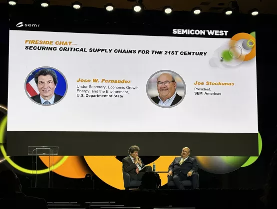
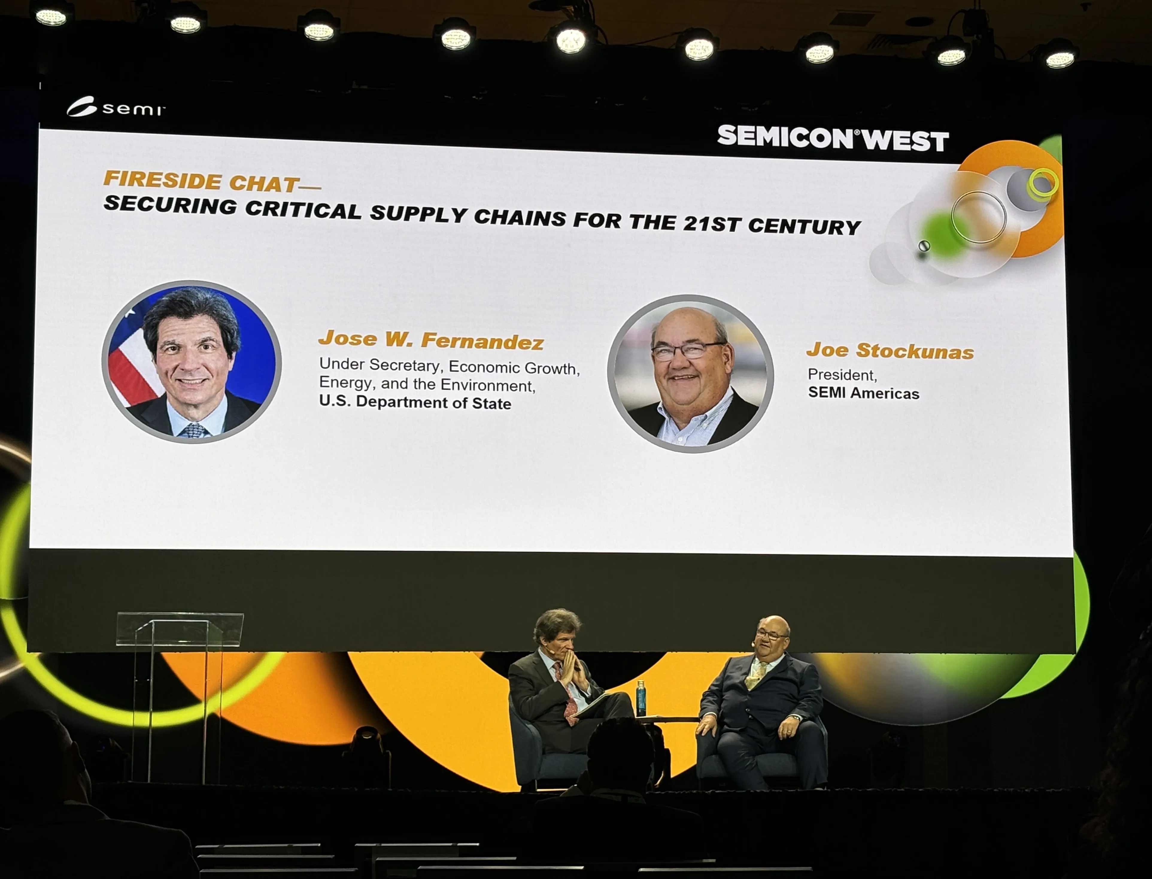
Jose Fernandez, U.S. Under Secretary of State for Economic Growth, Energy, and the Environment, sat down with Joe Stockunas, President of SEMI Americas, for a fireside chat on the CEO Summit keynote stage at SEMICON West 2024. In the Securing Critical Supply Chains for the 21st Century discussion, Fernandez emphasized the need to form partnerships to address vulnerabilities as the key to creating stable supply chains. It’s important to band together, he said, to protect our standards, values, and democracy. Diversifying the Global Mineral Supply ChainBecause chip fabricators depend on minerals like germanium, gallium, arsenic, indium, and rare earth elements, he highlighted how imperative it is for the industry to access them sustainably. To accomplish this, he stressed the importance of protection against supply chain bottlenecks in the mineral market. “According to a number of experts, we’re going to need 42x the amount of lithium by 2050, 25x the amount of manganese, and 25x the amount of cobalt,” he said. “Those minerals are basically controlled by one country, and that's a vulnerability.”To address these concerns, he shared that the State Department is working to strengthen the upstream and downstream portions of the semiconductor value chain, with the goal of supporting economic security across the globe. Foreign export controls, he said, have led to supply chain disruptions of key minerals, and bans on rare earth elements, processing equipment, and other technologies. As evidence of the State Department’s efforts to diversify, he highlighted the Minerals Security Partnership (MSP) and its work to seek mineral alternatives. Led by the U.S., it currently includes 13 other countries plus the European Union. Partnership and Investment Opportunities To further secure the industry's supply chain, Fernandez discussed the State Department’s efforts to partner with mining countries with untapped semiconductor resources. These countries, he said, also want alternate options for securing critical minerals. Fernandez highlighted Latin America as a key nearshoring focus area, pointing to the Americas Partnership for Economic Prosperity (APEP) as a solution for addressing obstacles to investment in the region. Obstacles, he said, include education levels, insecurity, and rule of law.To overcome such hurdles, he stressed the importance of fostering economic conditions that will attract investments, emphasizing the importance of workforce development initiatives and private sector involvement. “We don’t have enough trained workers in the U.S., and we certainly don’t have enough trained workers abroad,” he said. Fernandez shared that workforce development programs are being established through the U.S. Department of State International Technology Security and Innovation (ITSI) Fund, as well as private sector efforts and university partnerships. Currently, seven countries have been selected for ITSI funding, he said. “We’ve partnered with a number of universities to address the workforce gaps we see in our ITSI partners,” he said. “We’ve created workforce seminars, and we’re going to spend more time training the labor force.” These efforts supplement the work of the SEMI Foundation to develop a holistic workforce development program for the global semiconductor industry.Preventing Chips From Entering RussiaWith U.S. chips crossing into Russia through third parties, Stockunas asked Fernandez how the semiconductor industry could help address this. Despite existing sanctions against Russia, Fernandez shared that Russia still managed to import $1.7 billion worth of microchips from both the U.S. and Europe in 2023. To help slow this down, he highlighted additional due diligence for companies whose products often make their way into the country. The federal government, he said, speaks with these companies about complying beyond what the law requires.Fernandez shared that private sector cooperation with more stringent standards has been positive, noting that some companies have cut hundreds of distributors to further aid in prevention. In addition, he mentioned that sanctions have made a promising impact overall.“[Russia] has had to use outdated equipment, they’re engaging in counterfeiting, and they’re getting help from other countries,” he said. ​​Official SEMICON West Podcast In a podcast with Francoise von Trapp of 3D InCites recorded at SEMICON West, Fernandez discussed critical mineral partnerships, benefits and setbacks of regional supply chains, and chip sanctions against Russia. To learn more, check out the podcast interview with 3D InCites. SEMI Global AdvocacyDiscover how SEMI Global Advocacy Public Policy supports the microelectronics industry across trade, taxes, talent, and R D.John Cooney is Vice President of Global Advocacy and Public Policy at SEMI.
Read More
As more than 400 speakers took the stages at SEMICON West 2024, sustainability and workforce development stood out as two major focus areas. The second day of this year’s CEO Summit keynote program, themed Seizing the Global Opportunities and Challenges Ahead, featured sessions on both topics. One of the first sessions of the day was the Chief Sustainability Officer (CSO) panel discussion, titled Bracing for the Evolving Global Risk for the Semiconductor Ecosystem, moderated by Vice President of SEMI Global Sustainability Programs, Dr. Mousumi Bhat. Later that morning, Shari Liss, Vice President of SEMI Global Workforce Development Programs and Executive Director of the SEMI Foundation, moderated a fireside chat, Advocating for Real Change: Why Inclusion and Belonging Need to be Everyone’s Concern, with Sandra Mahadwar from KLA Corporation. Bhat and Liss were later interviewed for a podcast by Francoise von Trapp of 3D InCites to share additional insights on sustainability and workforce development, respectively. Bhat was also joined by Paul Kelly, COO of the New York Center for Research, Economic Advancement, Technology, Engineering, and Science (NY CREATES). Creating a More Sustainable Semiconductor Industry During their interview, both Bhat and Kelly emphasized that the industry will need to reduce its use of per and polyfluoroalkyl substances (PFAS) to sustainably innovate at today’s nanometer pace. For this reason, Kelly highlighted the importance of learning to balance current production demands with the health of climate.To achieve this balance, they discussed the efforts of the Semiconductor Climate Consortium (SCC). Much of the SCC’s efforts, they said, will focus on driving the industry toward net zero emissions. SEMI and NY CREATES announced a memorandum of understanding (MOU) at SEMICON West 2024 to promote sustainable practices within the industry, with a focus on PFAS reduction. Kelly pointed to the ability of SCC members to test new materials, gases, and chemicals at NY CREATES’ R D facilities in upstate New York to work toward replacing PFAS with more sustainable alternatives. Bhat also shared that this collaboration helps facilitate prototyping, experimentation, and tests and measurements for newer, more sustainable substances.Dr. Mousumi Bhat of SEMI and Dave Anderson of NY CREATES celebrate their organizations’ sustainability MOU at SEMICON West 2024.“The thought leadership comes from the Consortium, and the support on infrastructure comes from NY CREATES,” said Bhat. “This should become a blueprint to solve some of the challenging problems that we have in our industry.” When it comes to reducing emissions, Bhat mentioned two key objectives. The first, she said, is access to clean energy, and the second is the reduction of greenhouse gases. Bhat cited these as the issues that will take the longest for the industry to solve and pointed to the importance of industry collaboration and partnerships to support the needed experimentation. But while partnerships will bring the industry closer to net zero, both Bhat and Kelly cautioned that it won’t be reached overnight. “Much more needs to be done in the industry to reach that net zero goal,” said Kelly. “New chip technologies, new chemicals, and new processes are very much large leaps to achieving that. But right now, even some of the most advanced will only reduce [emissions] by 70%.” To help bridge this gap, Bhat encouraged others to join and participate in the SCC. “Rather than everybody doing a one-to-one experimentation in their own space and spending those resources, I would like to invite anyone that's not part of the climate consortium,” she said. “And [I invite] those that are part of the climate consortium to engage more actively, so that we are all accelerating the journey toward net zero.” Addressing the Talent Shortage This year’s SEMICON West also featured five keynote sessions dedicated to workforce development, as well as a Workforce Development Pavilion that included several talks around diversity, equity, inclusion, and belonging (DEIB). With the estimated one million jobs the industry will need to fill by 2030, Liss shared that every role is needed – from entry level all the way to Ph.D. researchers. “We need to try and bring in as many people as we can over the next few years,” said Liss. “The talent shortage is a global issue, not just a U.S. one.” Shari Liss of SEMI moderated the fireside chat at SEMICON West 2024 with Sandra Mahadwar from KLA Corporation.To begin to close the talent gap, Liss stressed the importance of educating children about the semiconductor industry. “We are just invisible to kids,” she said. “In every part of the globe, they carry chips in their hands all day every day, and they don’t know. So to me, breaking that barrier and making sure kids know about our work as an industry is going to be so critical to making this successful.” Liss also highlighted differences in workforce development programs across the world, noting that what works in one region may not translate to another. For example, apprenticeships are widely embraced in Europe, she said, but they’re a fairly new practice in the U.S. Conversely, she shared that veteran-focused programs wouldn’t work for some regions, but they’re a “powerful win” in the U.S. Each SEMICON show across the world, she shared, includes similar workforce development and DEIB programming, in addition to targeted sessions for students and HR professionals. Companies can interview for open positions at SEMICON shows as well. To learn more about SEMI’s workforce development initiatives and programming, visit semi foundation.org, or check out this overview of DEIB content at SEMICON West 2024. Samer Bahou is director of Marketing Communications at SEMI.
Read More
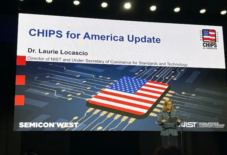
SEMI was honored to welcome U.S. Under Secretary of Commerce for Standards and Technology, Dr. Laurie E. Locascio, to the CEO Summit keynote stage at SEMICON West 2024 on Tuesday, July 9. Locascio, who also serves as the Director of the National Institute of Standards and Technology (NIST), delivered her morning CHIPS Act Update keynote address to a packed room of over 1,000 attendees at the Moscone Center in San Francisco.During her address, Locascio emphasized how far the U.S. chip industry has progressed since 2021. “Prior to 2022 and the passage of the CHIPS and Science Act, the U.S. produced 0% of the world's leading edge chips,” she said. “But now, after these proposed investments, we've changed the global landscape.”Industry Shifts from the CHIPS and Science ActDue to long delays and price increases resulting from supply chain vulnerabilities, Locascio shared that Congress began developing the CHIPS and Science Act with two key goals in mind. The first, she said, was to protect economic security, and the second, was to lower costs for American taxpayers. As part of the CHIPS and Science Act, CHIPS for America was established to advance semiconductor manufacturing in the U.S. CHIPS for America encompasses two offices: The CHIPS Research and Development Office, as well as the CHIPS Program Office - both of which are responsible for implementing CHIPS and Science Act law.CHIPS for America, said Locascio, couldn’t be another procurement program. Instead, it needed to be a purpose-driven approach to build domestic manufacturing capacity. Locascio highlighted that CHIPS for America galvanized several experts from the federal government, R D, and other core areas to work together to revitalize the U.S. semiconductor industry and increase capacity. To achieve this, Locascio pointed to CHIPS for America’s $30 billion in proposed direct funding and $25 billion in proposed direct loans.Locascio also noted diversity of technology as being essential for the American chip industry, citing how Intel, Micron, TSMC, and Samsung have recently expanded in the U.S., with SK Hynix planning to build a fab and R D facility in Indiana. No other economy in the world, she said, has more than two of these companies producing leading edge chips on its shores.“The total public and private investment from our four, leading-edge companies will equal roughly $300 billion between now and the end of the decade, far and away the most investment in new production in the history of the U.S. semiconductor industry,” said Locascio. Industry Investments on the HorizonTo further aid these efforts, Locascio mentioned CHIPS for America’s notice of intent to invest $1.6 billion in an open competition to accelerate advanced packaging domestically and encourage innovation. Funding will be directed toward five key R D areas, including equipment tools, power delivery, connector technology, chiplets, and Electronic Design Automation (EDA), she said. Additionally, Locascio shared that CHIPS for America recently announced its first preliminary memorandum of terms (PMT) to support the upstream supply chain, and shared plans to announce several more PMTs in the future. Lastly, Locascio revealed that CHIPS for America plans to release a model and process for bringing new facilities to life, in partnership with the National Semiconductor Technology Center (NSTC). NSTC members, she said, will gain access to partnership funds and state-of-the-art facilities to support the U.S. semiconductor industry. “Across all these efforts, from manufacturing incentives to research funding, to workforce development efforts, the U.S. must cultivate and build our competitive assets to protect and grow our technological leadership,” said Locascio.In a podcast with Francoise von Trapp of 3D InCites recorded at SEMICON West, Locascio discussed her career background, CHIPS Act investments and the path forward for the semiconductor industry in the U.S. To learn more, check out the podcast interview with 3D InCites. SEMI Global AdvocacyDiscover how SEMI Global Advocacy Public Policy supports the microelectronics industry across trade, taxes, talent, and R D.John Cooney is Vice President of Global Advocacy and Public Policy at SEMI.
Read More
Per- and polyfluoroalkyl substances (PFAS) are a large class of thousands of synthetic chemicals that are used throughout the semiconductor industry in the form of gases, liquids, and solid high-molecular weight polymers, due to their wide range of physical and chemical properties. PFAS contain carbon-fluorine bonds, which are one of the strongest chemical bonds in organic chemistry, allowing them to resist degradation and to cover long distances away from the source of their release.In recent years, the high persistence of PFAS in both the environment and the human body has encouraged the European Chemicals Agency (ECHA) to launch a PFAS restriction proposal aiming to regulate and eliminate their use over the next few years. The proposal is currently under assessment by ECHA’s scientific committees for Risk Assessment (RAC) and for Socio-Economic Analysis (SEAC).PFAS in the Semiconductor Industry The exceptional physiochemical properties of PFAS provide them a high degree of functionality in semiconductor manufacturing across the entire supply chain, and often the combination of their properties allows manufacturers to satisfy multiple and overlapping technical requirements.While the industry recognizes the importance of transitioning away from PFAS, and research to that effect is ongoing, current technological limitations do not allow the industry to manufacture semiconductors without the use of PFAS or to discover scientifically viable alternatives that can effectively substitute their use.At this point in time, no known alternatives exist for most of the uses of PFAS by the semiconductor industry. Alternative substances must be researched, invented and potentially applied into mass production to be recognized as viable alternatives. Many different pathways will have to be explored as PFAS are currently used across the entire supply chain for over 1,000 semiconductor applications, including articles, support equipment and fab operations, or as process chemicals.SEMI Europe—European Semiconductor Industry Association (ESIA) PFAS Research Workshop Considering the criticality of the PFAS issue for the semiconductor industry, SEMI and the European Semiconductor Industry Association (ESIA) have greatly strengthened their joint advocacy efforts over this past year concerning the ECHA’s PFAS restriction proposal.In this regard, SEMI and ESIA successfully organized a workshop in October 2023 with the relevant representatives of the European Commission (DG GROW, DG ENV, DG CNECT and DG RTD) to present and discuss in-depth the key technical evidence for the use of PFAS is the semiconductor sector. The discussions built upon the extensive technical evidence that was presented by SEMI and ESIA in their respective submissions for the six-month PFAS consultation facilitated by ECHA.Following the successful execution of this first workshop, there was a keen interest from the European Commission to enquire further upon the current state of play of research and development efforts in the field of PFAS detection, abatement, capture and destruction, circularity, recycling and alternativesFor this reason, after the first workshop, ESIA and SEMI collaborated to develop and deploy a joint PFAS Survey aimed at identifying the research priorities in PFAS from the perspective of their member companies. Based on the survey outcomes, the associations compiled the SEMI–ESIA PFAS Research Roadmap and officially presented it to the representatives of the European Commission during a follow-up workshop on 13th June 2024. Discussions at the workshop focused on the key research priorities for the semiconductor industry to discover potentially viable alternatives to the use of PFAS. In the upcoming legislative period, SEMI Europe will continue to engage with relevant stakeholders to contribute to the political debate and encourage a legislative framework that can enhance sustainability across industrial supply chains while preserving Europe’s technological competitive advantage. Get InvolvedGet involved in the SEMI PFAS Working Group! The SEMI PFAS Working Group is composed of industry technologists from leading companies across the global semiconductor manufacturing supply chain. The working group meets regularly to share intelligence and develop strategies to earn exemptions and/or extensions from regulators. Join SEMI in this crucial effort to enable the industry to continue manufacturing chips vital to the prosperity of the world by contacting [email protected]. Stefano Orlando is Manager Advocacy and Public Policy at SEMI Europe.
Read More
As the semiconductor industry works to attract talent to overcome its labor shortage, governments, educators, and the private sector must collaborate to make industry career opportunities more accessible for prospective employees. This concept provided the framework for a panel discussion during SEMI’s 35th annual Advanced Semiconductor Manufacturing Conference (ASMC) that took place in Albany, New York in mid-May.Despite extensive CHIPS and Science Act news coverage and escalating efforts to promote semiconductor career development initiatives, there’s still a tremendous amount of work to do, noted Fran Dillard, Vice President and Chief Diversity Inclusion Officer at Micron. “We're going to have to work to reduce barriers to this industry, and we have a chance to make a generational difference for American citizens,” she said. The panel, titled Talent Pipeline: Building a Sustainable and Diverse Semiconductor Workforce, featured Dillard and representatives from government and education who shared insights on growing the industry to fulfill unprecedented chip demand. Dillard was joined by Kylie Patterson, Chief Opportunity and Inclusion Officer at CHIPS for America; Kevin Younis, Chief Opportunity Officer and Executive Deputy Commissioner at Empire State Development; and Hector M. Rodriguez, Ph.D., Dean of Science, Technology, Engineering and Math at Hudson Valley Community College. Shari Liss, Executive Director of the SEMI Foundation, moderated the panel.Building the Future Together The need for extensive collaboration to bring semiconductor manufacturing back to the United States fueled the discussion. Patterson explained that given current investments in the semiconductor industry, the U.S. must double its workforce and triple its graduates in technical and construction-related fields. Overall, she estimated the industry will need to train around 100,000 new technicians.To achieve these goals, Rodriguez said that representatives from GlobalFoundries, the New York State Department of Labor, State University of New York, Center for Economic Growth, and the National Institute for Innovation and Technology, meet monthly to discuss on-the-job training programs for high school graduates and General Educational Development (GED) holders. He explained that by frequently evaluating training programs, they can quickly adjust curriculums if results don’t meet expectations. Younis said that bringing manufacturing back to the U.S. creates a unique alignment of interests between the government and the private sector. He highlighted the opportunity to work together to build the country’s manufacturing capacity, citing Empire State Development and Micron’s Green CHIPS Community Investment Fund for Central New York as an example of public and private collaboration. Part of the fund, he explained, will go toward workforce development. “We can focus on succeeding, with everyone marching in the same direction,” he said. Tapping Underrepresented Populations To find the talent needed to sustain the pace of semiconductor innovation, the panel stressed the importance of attracting people from all backgrounds and exposing them to the industry earlier in life. Dillard pointed out that women account for just 10-15% of workers in technical roles, and that percentage is even lower for people of color. “If we’re going to resource the semiconductor industry over the next 10-20 years, we’ve got to bring everyone with us,” she said.Helping those from underrepresented communities overcome barriers like limited access to childcare and transportation is important, said Rodriguez. He noted that wraparound services can be essential for transitioning these individuals into industry careers. Younis also highlighted Empire State Development’s One Network for Regional Advanced Manufacturing Partnerships (ON-RAMP) program, which will help provide these services in Upstate New York. If we’re going to get the people the industry needs, we must look for every opportunity, Rodriguez said, as they need to see that a great job is on the other side of the fence. Patterson said schoolchildren should be exposed to the semiconductor industry at a younger age, particularly girls and those from underrepresented groups. She cited a study about LEGO blocks, explaining that when the toy is introduced in primary school, boys are often excited, but girls are generally uncomfortable. “This is an example of the role of exposure,” she said. “If you’re not exposed to something, you have a lack of comfort, and that lack of comfort means you also have a lack of persistence to arrive at a level of competence.” Retaining the WorkforceAs an example of how to retain employees, Dillard pointed to the success of Micron’s Employee Resource Groups, as evidenced by the company’s internal data. These groups offer space for Micron’s underrepresented populations to connect with peers from similar backgrounds. Currently, the company has 10 groups, including groups for veterans, women, disabled employees, racial groups, and others. Diversity within leadership was also noted as key for retaining employees. Rodriguez said that when employees see people from similar backgrounds to their own in leadership roles, those employees are more likely to stay with those companies. Leadership training around psychological safety and working cross-culturally was also mentioned, with Dillard highlighting the importance of developing leaders that value inclusion. The cyclical nature of the industry was addressed during the Q A as a reason people may not stay long-term. Part of the solution, Patterson said, is to be transparent about market challenges and the importance of having a few months’ worth of savings. When employees encounter market challenges, they may be forced to switch industries if they don’t have savings to cover them. “There’s a role for us to be playing when it comes to supporting the financial literacy of our employees,” she said. View the full 2024 panel discussion to learn more. Additional ASMC 2024 HiglightsASMC 2024 featured keynotes by thought leaders from IBM, Wolfspeed, and Semiconductor Advisors. ASMC is the leading international technical conference for discussing solutions that improve the collective manufacturing expertise of the semiconductor industry. Solving the challenges presented by semiconductor manufacturing is a combined effort by device makers, equipment and materials suppliers, and academics. ASMC provides a platform for semiconductor professionals to network and learn the latest in the practical application of advanced manufacturing strategies and methodologies. Technical presentations at ASMC highlight industry innovations with specific results and select ASMC manuscripts are published in the ASMC Special Section of IEEE Transactions on Semiconductor Manufacturing.Krish Raghunath is Sr. Specialist for Conferences Committees at SEMI Americas.
Read More