downloadGroupGroupnoun_press release_995423_000000 copyGroupnoun_Feed_96767_000000Group 19noun_pictures_1817522_000000Member company iconResource item iconStore item iconGroup 19Group 19noun_Photo_2085192_000000 Copynoun_presentation_2096081_000000Group 19Group Copy 7noun_webinar_692730_000000Path
Skip to main content
Default Banner Image

semiconductors

The Rising Stars: 20 Under 30 blog series celebrates the brightest young leaders shaping the future of the semiconductor industry. These exceptional individuals have earned the SEMI Europe 20 Under 30 Award for making a remarkable impact across the supply chain—whether in engineering, sales, marketing, or R D. Nominations for the 2025 20 Under 30 Award are now open, providing the opportunity to recognize and honor the next wave of industry trailblazers.The series spotlights these rising stars for their career achievements, commitment to innovation, leadership skills, and dedication to driving both business success and community growth.Follow their inspiring journeys and discover how they are thriving and paving the way for future generations in the semiconductor world.Meet Anne-Mary Yeboah, Technology Manager at SoitecWith a background in materials science and a strong interest in technology, Anne-Mary Yeboah has built a career that connects the worlds of engineering and management. After earning her degree in engineering, she deepened her understanding of business through a Specialized Master’s in Management—an experience that broadened her perspective and prepared her for the challenges of a global, fast-moving industry.Today, as Technology Manager at Soitec, Yeboah leads projects that contribute to the next generation of semiconductor innovations. Her journey reflects a balance of technical curiosity, leadership growth, and a belief in the power of inclusion. In this interview, she shares her thoughts on career development, the importance of diversity, and how young professionals can find their voice in a rapidly evolving industry.SEMI: What inspired you to join the semiconductor industry? Yeboah: I’ve always been fascinated by technology, and semiconductors are at the core of innovation today. They are everywhere, from smartphones to electric vehicles, and being part of this field means contributing directly to the technologies shaping our lives and future.SEMI: How did your early experiences and education shape your career path?Yeboah: My engineering studies led me to specialize in materials science, which naturally included semiconductors. Later, I decided to expand my knowledge by pursuing a Specialized Master’s in Management. This combination of technical and business perspectives shaped my career path and ultimately brought me to Soitec, where I now connect both worlds as a Technology Manager.SEMI: Can you share a professional accomplishment you’re most proud of, and explain why it’s significant to you?Yeboah: I’m especially proud of starting my career directly as a Technology Manager. This role has allowed me to contribute to complex, strategic projects and collaborate with teams across functions. Working on products that will drive future innovations is deeply fulfilling and gives meaning to my work every day.SEMI: As a young professional in the industry, what is your greatest challenge? Yeboah: One of the biggest challenges has been finding my voice in a highly experienced environment. It can be intimidating at first, but I’ve learned to turn it into an opportunity to ask questions, learn quickly, and build confidence in my contributions. It has pushed me to develop a broad skill set and become an effective collaborator across teams.SEMI: What advice would you give to younger generations aspiring to make an impact in this industry?Yeboah: Dare to step forward and don’t create your own limits. Ask questions, even when you’re surrounded by experts, curiosity is a strength. Also, be patient. Building credibility and seeing your impact takes time, but each experience helps you grow and move closer to your goals.SEMI: How do you envision future work environments?Yeboah: I see the workplaces of the future as more innovative, inclusive, and collaborative. Diversity should be central, everyone should feel that their voice and perspective matter. At Soitec, initiatives like Women@Soitec are great examples of how gender equality and inclusion can empower people to thrive. I also believe technology and flexibility will continue to reshape how we work, helping us achieve both high performance and balance.SEMI: What impact has the 20 Under 30 Award had on your career? Yeboah: Receiving the 20 Under 30 Award has been a true honor and a wonderful source of motivation. It gave me a moment to reflect on how far I’ve come and to feel proud of my journey. The recognition has boosted my confidence, increased my visibility, and encouraged me to continue pushing forward in my career.Following 20 Under 30 JourneysAnne-Mary Yeboah’s story highlights the determination and adaptability driving today’s new generation of semiconductor professionals. Her ability to bridge science and management reflects the diverse skill sets shaping the industry’s future.The Rising Stars: 20 Under 30 blog series celebrates the exceptional talent and leadership driving the future of the semiconductor industry. Each of the young innovators honored is excelling in their respective fields while shaping the landscape of technology and business with their visionary approaches and dedication. Their stories exemplify the remarkable achievements and unwavering commitment that define the next generation of industry leaders. The series is intended to inspire and motivate future professionals to pursue their passions and embrace the opportunities within this dynamic industry. Stay tuned for more stories of rising stars who are paving the way for continued growth and innovation in the semiconductor world.Learn more about the SEMI Europe 20 Under 30 Award and the recipients honored at SEMICON Europa. SEMI ContactJames Lam, Business Development ManagerEmail: [email protected]
Read More
The Rising Stars: 20 Under 30 blog series celebrates the brightest young leaders shaping the future of the semiconductor industry. These exceptional individuals have earned the SEMI Europe 20 Under 30 Award for making a remarkable impact across the supply chain—whether in engineering, sales, marketing, or R D. Nominations for the 2025 20 Under 30 Award are now open, providing the opportunity to recognize and honor the next wave of industry trailblazers.The series spotlights these rising stars for their career achievements, commitment to innovation, leadership skills, and dedication to driving both business success and community growth.Follow their inspiring journeys and discover how they are thriving and paving the way for future generations in the semiconductor world.Meet Eloise Bond, Senior Etch Process Engineer at KLA Corporation (SPTS Division)Eloise Bond studied Physics at Swansea University before joining KLA in 2019 as an Etch Process Engineer. Since then, she has worked on cutting-edge semiconductor applications while actively promoting STEM through local outreach programs like Generation Tech.A proud recipient of the SEMI Europe 20 Under 30 Award, Bond shares how the recognition boosted her confidence and expanded her network, enabling her to take on new challenges. In her interview, she reflects on overcoming imposter syndrome, the value of flexible work, and the unexpected opportunities that shaped her career. Outside of work, Bond enjoys camping and bouldering.SEMI: What inspired you to join the semiconductor industry? Bond: I’ve always had a passion for science, so pursuing a career in a related field was natural. However, I wasn’t aware of the semiconductor industry until I began studying Physics at Swansea University, which has strong research ties with local semiconductor companies like KLA. Now that I am in the industry, I enjoy the hands-on aspects of my job. I find working with different materials and equipment is more engaging to me than an office-based job. SEMI: How did your early experiences and education shape your career path?Bond: STEM activities during my childhood and visits to museums with my parents sparked my interest in science and the physical world. That curiosity lead me to study physics at Swansea University, which ultimately paved the way to my current role at KLA. As I mentioned earlier, a career in semiconductors wasn’t really a conscious choice until relatively late in my education; I simply followed my passion for science. Today, I’m involved in many of the STEM outreach programs at KLA, helping to promote the semiconductor industry to young children so they can discover the same opportunities that I was fortunate to have had exposure to earlier in my life.SEMI: Can you share a professional accomplishment you’re most proud of, and explain why it’s significant to you?Bond: One accomplishment I’m particularly proud of is building strong customer relationships with a volume production fab in Korea. It was my first experience with direct customer interactions, which felt quite daunting at the time. I was invited to support a tool installation on-site, which allowed me to travel the furthest from the UK I had ever gone. Seeing firsthand how our tools fit into the wider industry gave me valuable context for my day-to-day responsibilities and made my work feel even more impactful. SEMI: As a young professional in the industry, what is your greatest challenge? Bond: Imposter syndrome has been a significant challenge for me. I often find myself in meetings with more senior colleagues and fear I am not performing well enough. However, over time, I have learned that my input is valid and that having multiple perspectives often leads to better outcomes.SEMI: What advice would you give to younger generations aspiring to make an impact in this industry?Bond: To make a difference, you first need to be part of the industry, just getting involved puts you in the room where conversations and decisions happen that you might not otherwise be exposed to.If an opportunity comes your way, take it. I entered this industry due to an opportunity presented to me at the end of my university career. KLA was my first real interview, and I honestly thought my chances were slim. I approached it as a ‘trial run’ and five years later, I’m still here. SEMI: How do you envision future work environments?Bond: I envision a new generation of management that places greater value on work-life balance. In many industries, senior management seem to have a relatively poor work-life balance, such as constantly doing business in the same way they’ve done for the past 40+ years – with constant business travel, working on holidays and long hours in the office. There is still an expectation for younger, ambitious employees to emulate this corporate culture, which creates barriers for those with caregiving responsibilities or other important commitments outside work. I believe a younger, more vocal generation of managers will drive positive changes in how we work. We will see more adoption of fully flexible working and 4-day weeks – happy employees lead to better work outcomes. I also think the technological advances which enabled the rapid switch to “working from home” during the COVID pandemic have permanently reshaped what is possible in terms of flexibly and efficiently.SEMI: What impact has the 20 Under 30 Award had on your career? Bond: This award has given me greater confidence to step outside of my comfort zone. It has also allowed me to increase my network to include colleagues I would have no reason to speak to previously. As a result, I have gained broader knowledge of how KLA operates as a whole and have been able to initiate small cross departmental projects I would not have been possible to before. Following 20 Under 30 JourneysEloise Bond’s journey highlights the passion, resilience, and forward-thinking mindset that characterize today’s emerging leaders in semiconductors. Her dedication to both technical excellence and community engagement showcases how rising stars are not only advancing the industry but also inspiring the next generation.The Rising Stars: 20 Under 30 blog series celebrates the exceptional talent and leadership driving the future of the semiconductor industry. Each of the young innovators honored is excelling in their respective fields while shaping the landscape of technology and business with their visionary approaches and dedication. Their stories exemplify the remarkable achievements and unwavering commitment that define the next generation of industry leaders. The series is intended to inspire and motivate future professionals to pursue their passions and embrace the opportunities within this dynamic industry. Stay tuned for more stories of rising stars who are paving the way for continued growth and innovation in the semiconductor world.Learn more about the SEMI Europe 20 Under 30 Award and the recipients honored at SEMICON Europa. SEMI ContactMaria Daniela Perez, Communications ManagerEmail: [email protected]
Read More
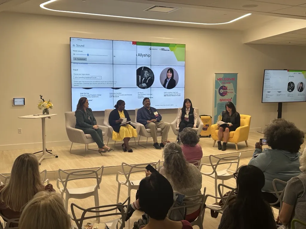
This year, the Women in Semiconductor (WiS) program takes a huge step growing nationally — hosting events in New York, Michigan, Ohio, California, and Arizona. Managed by the SEMI Foundation, the WiS program aims to highlight women’s contributions and leadership in the semiconductor sector and actively address the gender gap to support inclusive workplaces.Over the years, WiS has shifted from an abstract discussion to actionable strategies—focusing on skills like negotiation, strategic decision-making, storytelling, and career advancement. WiS also promotes allyship, inviting and including men to participate as advocates and supporters of women in the industry.Building on the program’s strong momentum, this year highlights the initiative’s growth and impact through expansion across multiple regions – focusing on the theme “Empowerment in Action: Real Strategies for Women’s Success” dedicated toward impactful, actionable programming.The first 2025 WiS program was held in Albany, NY, in conjunction with ASMC on May 8. New WiS programs are scheduled in the following locations:Ann Arbor, Michigan on September 16, 2025Willoughby, Ohio (date to be announced)San Jose, CA on November 20, 2025Phoenix, Arizona on December 11, 2025The WiS is supported by grants from the Kellogg Foundation and the David Lucile Packard Foundation. The programming is also aligned with SEMI Foundation’s Chips Childcare program, which supports childcare-access solutions to strengthen workforce participation—particularly for parents and caregivers. Learn more in our blog: Affordable, Accessible, and Quality Childcare: A Critical Workforce Development Strategy for the Semiconductor Industry.The WiS initiative has evolved into a powerful platform that blends strategic programming, mentorship, allyship, regionally accessible events, and support systems like childcare advocacy. It’s an inspiring example of how consistent focus and innovation can build meaningful change over nearly a decade. If you’re interested in getting involved, contact Bia Hamed at [email protected]. Bia Hamed, Ph.D., is Program Manager for Global Education Initiatives at the SEMI Foundation, focusing on educational programming that supports workforce pipeline building nationally and internationally.
Read More
The Rising Stars: 20 Under 30 blog series celebrates the brightest young leaders shaping the future of the semiconductor industry. These exceptional individuals have earned the SEMI Europe 20 Under 30 Award for making a remarkable impact across the supply chain—whether in engineering, sales, marketing, or R D. Nominations for the 2025 20 Under 30 Award are now open, providing the opportunity to recognize and honor the next wave of industry trailblazers.The series spotlights these rising stars for their career achievements, commitment to innovation, leadership skills, and dedication to driving both business success and community growth.Follow their inspiring journeys and discover how they are thriving and paving the way for future generations in the semiconductor world.Introducing Mariusz Grabowski: Lead Design Engineer at Cadence Design SystemsMariusz Grabowski, a 2023 20 Under 30 award recipient at the age of 24. He is now a Lead Design Engineer at Cadence Design Systems, Inc., where he’s been making strides in digital systems design for nearly three years. Prior to this role, he gained valuable experience as an FPGA Design and Verification Engineer at Aldec Inc. Grabowski holds a master’s degree with distinction in automation and robotics from AGH University of Science and Technology in Krakow, Poland. During his academic career, he was an active member of both the Avader and Integra Scientific Groups. He also achieved recognition at events like DASIP 2023 and in the International FPGA Hackathon, where he and his team earned 2nd and 3rd place. He is currently also pursuing a postgraduate degree in Project Management at SGH Warsaw School of Economics. SEMI: What inspired you to join the semiconductor industry? Grabowski: I have always been fascinated by the fundamental workings of advanced systems and that curiosity led me to pursue a career in the semiconductor industry. As a digital design engineer, it is exciting for me to contribute to the creation of such large and sophisticated architectures from basic building blocks. Now, I’m proud to be a part of Cadence Design Systems, where I can work on the cutting-edge designs with some of the most talented and hard-working engineers. Grabowski and his team at the awards ceremony at FPGA Hackathon 2023SEMI: How did your early experiences and education shape your career path?Grabowski: During my studies, I had the opportunity to work on hands-on projects with an FPGA platform, which led me to my first job as an FPGA design and verification engineer. That experience gave me a broader perspective on the industry’s scale and reinforced my passion for tackling challenges, learning and growing in this field.Grabowski presenting his paper at the DASIP 2023 ConferenceSEMI: Can you share a professional accomplishment you’re most proud of, and explain why it’s significant to you? Grabowski: For me, it is successfully balancing full-time studies with work. It was a challenging experience, but it provided invaluable opportunities to grow my skills and gain hands-on experience. During that time, I completed numerous projects, participated in scientific conferences and industry events like DASIP 2023, and even earned 2nd and 3rd place in the International FPGA Hackathon. These achievements reinforced my passion for the field and my ability to thrive under pressure. SEMI: As a young professional in the industry, what is your greatest challenge? Grabowski: One of the biggest challenges is navigating the complexity of large-scale projects, where seamless coordination between multiple teams across the globe is crucial. As someone still early in my career, gaining the experience to manage the cross-functional aspects of a project while ensuring my own contributions are technically sound has been both demanding and rewarding.Grabowski at the Discussion Panel on Industry Career Perspectives at DATE 2024 ConferenceSEMI: What advice would you give to younger generations aspiring to make an impact in this industry?Grabowski: The sheer amount of information and complexity in the industry can feel overwhelming. It is essential to embrace curiosity and continuous learning, but it is also crucial to recognize that you can’t do everything alone. My advice is to find your area of expertise and collaborate with others; teamwork is key to bringing impactful projects to life. Cadence’s Design Team in Warsaw, Poland Manager Jacek Rosiak—3rd from the leftSEMI: How do you envision future work environments? Grabowski: I envision future work environments as places where technology fosters creativity and collaboration, diversity is celebrated, and flexibility and work-life balance are prioritized. These environments will empower employees to perform at their best while feeling supported and valued. I am proud to be a part of Cadence Design Systems, where I feel that these values are strongly cultivated. SEMI: What impact has the 20 Under 30 Award had on your career? Grabowski: Receiving the 20 Under 30 Award was an incredible validation of the hard work I’ve put into my role. It gave me a confidence boost, affirming that I am on the right path and capable of making meaningful contributions to my company and the broader semiconductor industry. It also brought significant recognition, which opens up numerous opportunities.Following 20 Under 30 JourneysMariusz Grabowski’s journey in the semiconductor industry highlights the power of dedication, curiosity, and continuous learning. From his early experiences with FPGA platforms to his significant accomplishments in both academia and industry, Grabowski is a true example of how passion and hard work can drive meaningful contributions. As a young professional, his insights offer valuable inspiration for the next generation of engineers eager to make their mark in this ever-evolving field. With a bright future ahead, Grabowski is sure to continue influencing the world of technology, one innovative project at a time.The Rising Stars: 20 Under 30 blog series celebrates the exceptional talent and leadership driving the future of the semiconductor industry. Each of the young innovators honored is excelling in their respective fields while shaping the landscape of technology and business with their visionary approaches and dedication. Their stories exemplify the remarkable achievements and unwavering commitment that define the next generation of industry leaders. The series is intended to inspire and motivate future professionals to pursue their passions and embrace the opportunities within this dynamic industry. Stay tuned for more stories of rising stars who are paving the way for continued growth and innovation in the semiconductor world.Learn more about the SEMI Europe 20 Under 30 Award and the recipients honored at SEMICON Europa. SEMI ContactMaria Daniela Perez, Communications ManagerEmail: [email protected]
Read More
Even before the invention of the first semiconductor, women have been making significant contributions to technology. As of July 2024, 27.6% of the tech workforce identified as female. During the last 5 years, the percentage of women represented in tech increased by less than 3%. A bright spot is the semiconductor industry, where women comprise nearly 29% of the workforce. However, there’s still a long way to go until we see greater gender equity. Although women aren’t always highly visible in their roles, their achievements are significant. The slide show featured at the Women in Semiconductors (WiS) reception during SEMI’s Industry Strategy Symposium (ISS) 2025 earlier this month highlighted only a small number of the many women who have made a positive and lasting impact on technology. From Ada Lovelace, founder of scientific computing, to Lisa Su, AMD CEO who was named Time’s CEO of 2024, women have long been technology trailblazers and role models to inspire future female leaders.At this year’s WiS reception, attendees joined in a celebration of industry pioneers, both past and present. “When women come together, amazing things happen," said Shari Liss, SEMI Vice President of Global Workforce Development Initiatives. “The event was all about connection, mentorship, allyship, and lifting each other up. In a world that can feel heavy, it was a reminder of the strength we have when we support one another and work together to shape the future of our industry,” said Liss. WiS continues to be an important part of SEMI Foundation workforce development programming.Shari Liss, SEMI Vice President of Global Workforce Development and Initiatives at ISS 2025In her welcoming remarks, Debbie Gustafson, CEO of Energetiq Technology, Inc., a Hamamatsu Company and a member of the SEMI Foundation Board of Trustees, asked how many people in the audience feel that they can make a difference, and only half raised their hands. She shared a story of how she has made a difference by making her company realize the important role women play in bringing innovative solutions to today’s most pressing challenges. “Everyone can help improve the number of women in your companies by creating an effective place for women to have a personal life and also have a career!” Debbie Gustafson, CEO, Energetiq Technologies at ISS 2025This is the second year Energetiq has sponsored the WiS reception at ISS. “It’s a way to show my support for SEMI events and encourage men to attend as allies to women,” said Gustafson, as images of industry luminaries were projected on the screen behind her. She recalled her first ISS and how few women were in attendance. The gender gap has declined over the years, but the number of women, including speakers, at ISS and other SEMI programs remain low. “I hope that every one of the women and allies will volunteer and raise their voices,” urged Gustafson.Gustafson asked for additional comments from the audience, and SEMI President and CEO Ajit Manocha immediately volunteered to add his voice in support. “Our industry must do a better job of recruiting and retaining women – and most importantly – providing leadership opportunities,” said Manocha. “The benefits of diversity and female leadership to business operations and the bottom line are well documented. Women are crucial to narrowing the talent gap, and ultimately, to our industry’s future.”Celebrating Women in Semiconductors at ISS 2025Creating true inclusion and equity in the workplace is critical to everyone’s success. Since its inception almost a decade ago, Women in Semiconductors has highlighted women’s contributions and leadership in the semiconductor industry and recognizing the need to bridge the workplace gender gap. Our upcoming May 2025 program, which will be held in conjunction with ASMC, will highlight authentic stories to inspire and provide actionable insights. The agenda will include skills development which incorporates decision-making, strategic thinking, negotiation, as well as networking opportunities to connect aspiring leaders with experienced mentors who can provide guidance.In 2025, we’re excited to expand the WiS initiative to programs in Arizona, Michigan and Ohio with funding from the W.K. Kellogg Foundation and David and Lucile Packard Foundation. An important piece of this work is SEMI Foundation’s Chips Childcare program. Through Chips Childcare, SEMI Foundation partners with Policy Equity Group and other organizations across the country to support companies in designing stronger childcare plans and systems. Affordable, accessible, and quality childcare is a critical element of successful workforce development and paramount to not just helping families thrive, but ensuring that communities, cities, and the country can meet economic goals. Part of this program is providing industry awareness and outreach to women and parents who rely on childcare to work, and expanding Women in Semiconductors to new regions will support Chips Childcare goals. Learn more about the Chips Childcare program in SEMI’s blog: Affordable, Accessible, and Quality Childcare: A Critical Workforce Development Strategy for the Semiconductor Industry.”Companies that embrace inclusion, leveraging the strengths of all workers – including women – create dynamic and innovative work environments. We encourage everyone in the industry to focus on steps they can make, collectively or individually and regardless of position, to drive meaningful progress to advance women and a thriving semiconductor industry.The next WiS event will transition beyond discussions to providing practical strategies that can help women secure internal job opportunities and build skills needed for career advancement, and how can we empower changes that lead to meaningful improvements that drive lasting impact for everyone. Learn more about empowering change at Women in Semiconductors on May 8, 2025. For details, visit https://www.semi.org/en/connect/events/women-in-semiconductors-wisMargaret Kindling is Senior Program Manager at the SEMI Foundation. She promotes inclusive workplaces via initiatives like WiS, Semiconductor PRIDE and workforce development programming at SEMICON West and SEMIEXPO Heartland.
Read More
The Rising Stars: 20 Under 30 blog series celebrates the brightest young leaders shaping the future of the semiconductor industry. These exceptional individuals have earned the SEMI Europe 20 Under 30 Award for making a remarkable impact across the supply chain—whether in engineering, sales, marketing, or R D. The series spotlights these rising stars for their career achievements, commitment to innovation, leadership skills, and dedication to driving both business success and community growth.Follow their inspiring journeys and discover how they are thriving and paving the way for future generations in the semiconductor world.Introducing Raphael Hardegger: Product Manager Advanced Products at VATRaphael Hardegger is a Product Manager at VAT, where he leads the development of innovative atomic layer deposition (ALD) valve technology. Starting his career in 2009 as a design engineer apprentice at VAT, Raphael has since gained diverse experience, including entrepreneurial ventures and a role in MedTech. Today, he focuses on shaping product strategy, aligning solutions with customer needs, and driving impactful advancements in the semiconductor industry.SEMI: What inspired you to join the semiconductor industry? Hardegger: I joined the semiconductor industry, and VAT in particular, at the young age of 15. Back then, I started as a design engineer in VAT’s apprenticeship program. Growing up in the beautiful VAT region, my entry into the industry was somewhat by chance – but I’m incredibly glad it happened! After gaining foundational knowledge at VAT, I pursued studies in mechanical engineering, worked in various other roles and companies, and then completed a master’s in business innovation. About 3.5 years ago, the semiconductor industry pulled me back in, and I haven’t looked back since. What keeps me excited about VAT and the industry as a whole is its sheer complexity. Every day, we have the opportunity to innovate with small components that have a significant impact on a huge industry. It’s such a multifaceted field that I’m confident I’ll continue learning something new every day for the rest of my career.SEMI: How did your early experiences and education shape your career path?Hardegger: In Switzerland, the apprenticeship model uses a results-oriented work style from an early age. The lessons I learned during my four years as an apprentice at VAT continue to influence my daily work life. The mechanical foundation I built during that time remains a tremendous asset in my career. When combined with my studies in systems engineering and business innovation, this foundation has allowed me to make a meaningful impact both at VAT and within the broader industry.SEMI: Can you share a professional accomplishment you’re most proud of, and explain why it’s significant to you? Raphael Hardegger in the VAT office of San Jose, California, USA, holding the new product he worked on.Hardegger: When I rejoined VAT as a product manager, I was given the opportunity to manage a new product that wasn’t even on the market yet. This product was a key part of VAT’s strategy to outpace market growth by expanding into new product segments beyond our core offerings. I had the privilege of collaborating with some of VAT’s most talented engineers, who developed an incredible product. Together, we learned a great deal through our initial interactions with customers, refining the product to meet stringent requirements. This year, we successfully qualified the product for use in the industry’s most challenging semiconductor processes. It’s a testament to how dedication, customer-focused engineering and exceptional teamwork can make a significant impact. What makes me proud is not just working on innovative concepts, but creating products that truly excite our customers and contribute to meaningful growth for VAT.SEMI: As a young professional in the industry, what is your greatest challenge? Hardegger: I turned 30 this year, so I suspect I was one of the oldest 20 under 30 winners last year. One challenge I’ve faced — not only in this industry, but across others — is impatience. As a young professional with high aspirations, it’s easy to feel that things aren’t moving fast enough. We often expect early promotions, annual salary increases, and quick recognition for our efforts. What changed my perception on this was a conversation with a senior manager at VAT shortly after I joined. I asked him what steps I should take to move closer to my next career goal, such as earning a management position. His response was simple and direct: Focus on making an impact in your current role. Build a strong track record and demonstrate your skills. Everything else will follow. I took his advice, and I'm glad I did. No, I didn't get promoted immediately, but I learned the value of patience, doing my best every day, and finding satisfaction in the process.Career progression isn’t just about motivation and talent — it’s also about timing and aligning with the business needs. Being impatient or pushing for premature career moves can often backfire, leaving you in a worse position than before. By focusing on making a genuine impact and building a solid track record, you create a strong foundation for a fulfilling and sustainable career.SEMI: What advice would you give to younger generations aspiring to make an impact in this industry?Hardegger: You're in a great place — right where you need to be. Be curious and explore as much of the semiconductor industry as you can. During my training as a design engineer, I wasn't deeply involved in understanding the customer applications our valves were serving. My focus was primarily on developing vacuum valves based on product management requirements and manufacturing needs. Since I returned, I've learned the importance of understanding what our customers truly need and translating those needs into product requirements.This shift has not only helped me and the team create better products, but also made the work much more enjoyable! While I'd still like to deepen my understanding of customers' processes, it's already fascinating to learn more about their goals and see how our products can make a real difference. If I could go back to my apprenticeship or just starting this industry, my advice to myself — and to anyone starting out — would be to stay as curious as possible. Take every opportunity to learn what customers are trying to achieve with the products you help create. That curiosity will guide you to make a meaningful impact.SEMI: How do you envision future work environments? Hardegger: To me, having a clear customer focus in every aspect of a company's efforts is essential. At the end of the day, someone needs to want to buy our products for us to remain profitable and continue to grow. That’s why maintaining a customer-centric approach in all aspects of product development and management is critical. At the same time, the people who work in such companies need to be happy and fulfilled to create great products. I appreciate the recent trends we’re seeing to improve the corporate culture, such as embracing hybrid working models. These approaches provide a healthy balance between in-office collaboration and focused work from home, helping employees maintain productivity and well-being.SEMI: What impact has the 20 Under 30 Award had on your career? Hardegger: While I deeply appreciate the recognition that comes with such awards, I believe my career should ultimately be defined by the impact I make in my field. That said, I do hope the award inspires other young professionals to explore this exciting industry and build meaningful careers here! Following 20 Under 30 JourneysRaphael Hardegger’s journey in the semiconductor industry is a testament to the power of curiosity, dedication, and a customer-centric approach. From his early days as a design engineer apprentice to his current leadership in product innovation, Raphael continues to drive meaningful change at VAT Group. His story inspires young professionals to embrace continuous learning, focus on making a real impact, and contribute to the growth and success of the semiconductor industry.The Rising Stars: 20 Under 30 blog series celebrates the exceptional talent and leadership driving the future of the semiconductor industry. Each of the young innovators honored is excelling in their respective fields while shaping the landscape of technology and business with their visionary approaches and dedication. Their stories exemplify the remarkable achievements and unwavering commitment that define the next generation of industry leaders. The series is intended to inspire and motivate future professionals to pursue their passions and embrace the opportunities within this dynamic industry. Stay tuned for more stories of rising stars who are paving the way for continued growth and innovation in the semiconductor world.Learn more about the SEMI Europe 20 Under 30 Award and the recipients honored at SEMICON Europa. SEMI ContactMaria Daniela Perez, Communications ManagerEmail: [email protected]
Read More
The semiconductor industry continues to push the envelope to meet demands of key applications such as advanced computing, consumer electronics, and defense, as well as environmental sustainability. There remain several critical challenges that our industry is working diligently to address, but how can these issues be tackled more effectively and at a pace that can keep up with this ever-evolving landscape?SEMI sat down with Supika Mashiro, Advisor at Tokyo Electron, where she shares her perspective on the importance of strengthening industry collaboration and what SEMI is doing through its first-ever SEMI Global Standards Summit – “Innovating Tomorrow: Standards for Future Factories” – of which she chairs the Planning Committee responsible for organizing this Summit.Trio: What is the SEMI Global Standards Summit and why is this event timely?Mashiro-san: Topics such as advanced packaging, cybersecurity, as well as supply chain and materials innovation (and their impact to the environment) are considered strategic areas requiring more industry collaboration. Many of these areas also greatly benefit from standards, and the next generation specifications and guidelines will need to be engineered to meet the technical challenges we face today and in the future. The magnitude of these standardization efforts will require engagement from all stakeholders in the design-to-manufacturing value chain as well as multiple Standards Developing Organizations (SDOs) coordinating and collaborating with each other.This is the driving force behind the Summit, and the need to bring together industry stakeholders to identify standards-critical areas and align on developing an industry standardization strategy for the next 3- and 7-year time horizons. We are excited to host this inaugural event on December 12, 2024, in conjunction with SEMICON Japan 2024. Trio: What is the focus of the Summit?Mashiro-san: The Global Standards Summit will cover three main themes: Smart Manufacturing for Future Factories, Packaging Architectures Materials, Environmental Sustainability.Factories are increasing their use of digital twins, predictive maintenance, and AI/ML to improve productivity and yield across the entire manufacturing environment. To take full advantage of these approaches, factories must reduce cybersecurity risks and secure the transfer of “smart” data across the entire supply chain while protecting IP. There is a need for standards to address these risk areas, as well as help diverse advanced analytics systems interoperate to assist personnel in increasing factory productivity. In the Smart Manufacturing for Future Factories session, we will be focusing on autonomous fabs, cybersecurity, and flow-oriented manufacturing.Similarly, packaging technologies have been progressing since the early stages of semiconductor device development more than 70 years ago. More recently, where packaging occurs in the semiconductor process has evolved, and some of the packaging processes are now done as an extension of front-end manufacturing. Moving forward, packaging architecture and materials are becoming increasingly important, driven by the adoption of heterogenous integration to address demands for more complex functionality and reduced power consumption as well as enabling chiplet integration. In the Packaging Architecture Materials session, we will discuss what kind of standardization our industry requires for copper-copper (Cu-Cu) direct interconnection, hybrid bonding, and panel-level packaging. We will also explore glass substrates as well as standards needed to enable semiconductor assembly and test automation.Our third session recognizes that the semiconductor industry is heading into an era of NetZero, in which quantification of environmental performance can have meaningful financial impact. The methods of measuring and accounting the environmental impact such as carbon emissions and the presence of substances of concern in manufacturing and products are not uniformly consistent across the industry. In order for the semiconductor industry to better navigate and make a positive impact in this arena, a consistent set of standards will be crucial. In the Environmental Sustainability session, thought leaders will present on communicating substance of concern (SOC), reporting of process emissions from factories, as well as lifecycle assessment of materials and substances used in semiconductor manufacturing, including equipment.Last but not the least, we will feature a panel session where we will explore all of these topics in a discussion with our panelists.Trio: Who should attend the Summit and why?Mashiro-san: The Summit is intended for leaders who are interested in these standardization topics to come and engage. Attendees will hear and learn about the issues critical to the future advancements of semiconductor manufacturing, what’s happening to address them, as well as new standards development. Attendee engagement is critical as we want our participants to influence and be able to contribute to the direction of standards development by providing valuable insights to help optimize future factories. To facilitate industry collaboration, we have organized networking events with other stakeholders from suppliers and solutions providers to end customers. The Summit is just one of many compelling reasons for industry stakeholders and thought leaders to come to SEMICON Japan. There are several sessions on many related topics that we are covering in the Global Standards Summit. Ultimately, at the conclusion of the Summit, we expect to have identified lists of critical standards areas, and we would like for those leaders to be able to assign and dedicate resources to these standardization efforts.For more information about the inaugural SEMI Global Standards Summit, please visit the SEMICON Japan 2024 site and register today!Supika Mashiro works as an Advisor for Strategic Planning of Industry Initiative Group at Tokyo Electron Limited.She has been involved in Factory Integration (FI) IFT of IRDS since its inauguration in 2016 and a co-chair since 2017. Her area of interest and involvement encompasses “smart” technology applications in manufacturing equipment, its co-optimization with Fab operation as well as ESH/S (Environment, Safety, and Health/ Sustainability) road-mapping and related industry standard development. For the latter, she has taken a couple of leadership roles in SEMI Standards Program as well as IEC TC/44.Paul Trio is Director of the SEMI Standards program.
Read More
Gone are the days when companies were said to go “beyond compliance” if they had sustainability ambitions and operated in a largely voluntary space.Corporate sustainability now sits in a tangle of business priorities, stakeholder expectations, and regulatory obligations. New landmark legislation and policies have changed the game in many markets where semiconductor value chain companies do business. Today, accuracy of information, threshold-setting, evaluation criteria, and due diligence are subject to scrutiny, fines, and litigation.A myriad of compliance risks are now linked to business actions that were historically voluntary in a sustainability context. Fueling the shift are regulations such as the EU’s Corporate Sustainability Due Diligence Directive (CSDDD) and Corporate Sustainability Reporting Directive (CSRD).Across the semiconductor value chain, it is crucial for companies to have a solid regulatory strategy for their sustainability activities. They must take into account, for example, mandatory rules that drive up risks from selectively taking action on some sustainability issues while demoting others.Semiconductor manufacturing and design firms, together with their business partners, face heightened pressure to navigate business and sustainability priorities around the climate transition, human capital management, supply chain management, and a host of other environmental, social, and governance issues that are high on regulatory agendas.The SEMI Sustainability Initiative hosts several working groups that bring to light common concerns and provide a forum for sharing response strategies. To sharpen the guidance that SEMI offers, the Sustainability Initiative is launching the webinar series, Global State of Play: Sustainability Regulations, Reporting, Incentives. This series offers semiconductor industry professionals the chance to learn from top-tier experts on the most pressing challenges in compliance, disclosure, and strategy for sustainable business.The first webinar, Developing a Regulatory Strategy for Sustainability: How to Navigate Key Sustainability Decisions, will feature Ashley Walter, Partner and Chief Sustainability Officer at Orrick Herrington Sutcliffe LLP.As the global business association for the electronics design and manufacturing value chain, SEMI is pleased to convene experts to address improving sustainability strategies for our industry. The SEMI Sustainability Initiative invites industry stakeholders to see the importance of building a regulatory strategy that coordinates across functions, from engineering to the boardroom.Learn more and register.Jordan Famularo, PhD, is Programs Manager, Sustainability at SEMI.
Read More
The Rising Stars: 20 Under 30 blog series celebrates the brightest young leaders shaping the future of the semiconductor industry. These exceptional individuals have earned the SEMI Europe 20 Under 30 Award for making a remarkable impact across the supply chain—whether in engineering, sales, marketing, or R D. The series spotlights these rising stars for their career achievements, commitment to innovation, leadership skills, and dedication to driving both business success and community growth.Follow their inspiring journeys, and discover how they are thriving and paving the way for future generations in the semiconductor world.Introducing Marieke Vermeulen: Product Quality Assurance Engineer at MelexisMarieke Vermeulen's journey into the semiconductor industry is a testament to curiosity, adaptability, and self-driven learning. With a background in classical philology, her entry into Melexis as a customer quality technician was unexpected, yet she quickly embraced the challenges of the industry. Through her commitment to growth and innovation, Marieke has risen to the role of Product Engineer, demonstrating leadership and a passion for continuous improvement. Her contributions, particularly in product ownership and driving business growth, highlight her as a dynamic force within Melexis, embodying both technical excellence and a collaborative spirit.SEMI: What inspired you to join the semiconductor industry? Vermeulen: My entry into the semiconductor industry was actually quite accidental. After completing my master’s degree in classical philology, I was still unsure about which direction I wanted my professional life to take. Then, an opportunity arose to join Melexis as a customer quality technician.I did not have anyone in my immediate circle with experience in the industry, so I entered the field without really knowing what to expect. I had only a vague idea of what a semiconductor company did. However, from those early days onwards, I have not looked back. It is my love of knowledge and the desire for a deeper understanding that continues to drive me in my role within Melexis’s quality department. During my literature studies, I was motivated by the idea that there is no absolute, uncontestable truth. Meaning will change with time and place. This perspective aligns closely with the mindset of the semiconductor industry. With new inventions and concepts constantly emerging, the industry is always evolving. We must challenge what we believe to be true yesterday and adapt to the discoveries and advancements for today.So, while there was no direct inspiration that led me to join, more of a stumble into the field, I have since developed a deep respect for how the industry operates. I In particular, I respect how people in the industry do not hesitate to question in order to keep pushing the boundaries of innovation.SEMI: How did your early experiences and education shape your career path?Vermeulen: There was no direct experience. During my school years, STEM was just beginning to earn its place in my educational framework, and we were only introduced to the basic principles. Fortunately, this has changed significantly since then. However, my background hasn’t held me back, in fact, quite the opposite.One main principle from my studies stands out: in language, nothing is set in stone. There is no single truth, no single solution and no single voice. At its heart, language is shaped by human interaction. My studies taught me to think critically and to understand that there is always more than one answer to a question. This approach directly influences the way we work in the product quality department. Our goal is to develop and produce products that meet a customer’s needs as closely as possible. But it is a continuous process and very rarely a straight line. We learn from our past experience to improve the next iteration, again and again. We regularly consult with our peers to gather different ideas, and we listen to the industry to understand where the needs are. Then, we translate those insights into an effective solution.SEMI: Can you share a professional accomplishment you’re most proud of, and explain why it’s significant to you?Vermeulen: Our products go through two main stages in their lifecycle: development and production. As a product engineer, I am responsible during the production stage. However, before we reach this point, there is a transition period where the development and production teams come together to prepare the product for the best possible launch. This period is often hectic, but it clearly demonstrates how much of a team effort our products represent. Every team member understands their role and works towards the collective goal. Being part of such a diverse team and seeing our products succeed is always a thrill for me. While the products are made with metals, silicon, and other elements, it is the human factor that truly brings them to life. The very first spark is always the idea to create. SEMI: As a young professional in the industry, what is your greatest challenge? Vermeulen: As a young woman in STEM, the most obvious answer is that I have to prove myself more than my male colleagues or more experienced peers. However, at Melexis, I have found strong support in overcoming this challenge. Our voices are heard, and we are an active and valued part of our teams. We can express our ideas freely, knowing they will be considered just as seriously as anyone else’s. I can only hope this trend continues throughout the industry.SEMI: What advice would you give to younger generations aspiring to make an impact in this industry?Vermeulen: To those who are unsure if STEM is truly for them, I would say: We need engineers, but we also need dreamers to bring the ideas to life. We need designers and coders who can make the device function, but we also need people who can communicate these concepts to the world. Moreover, we need educators who can inspire and teach the next generations. There is a place for many different minds within the industry, so I encourage you to step in this direction. I’m sure you will find a place.And for those inspired by the semiconductor world and are sure this is where they want to be: don’t be afraid to look beyond the industry. Listen to those around you and take their ideas to heart. Be the inventor for those who cannot bring ideas to life, and offer solutions to those who feel stuck.Cooperation has made our industry great, and it is essential for building a strong foundation moving forward. SEMI: How do you envision future work environments?Vermeulen: The past few years have demonstrated how advanced technology has made the world much smaller. With just a click of a button, a camera, and a microphone, we can connect to the world, ignoring the constrains of time, space and borders. This accessibility opens the door for many more people to enter the industry from all around the globe. A hybrid and flexible work environment enhances this even further, accommodating those who might face physical or logistical restrictions. We need to continue on this path. By embracing diversity, we allow new ideas to emerge at the intersection of different minds. Why exclude a brilliant mind simply because they are on the other side of the continent? Why overlook someone whose mother tongue differs from yours when we can find a common language?At Melexis, we already welcome many different cultures, and it is amazing to see how vibrant this makes our offices. New team members bring their own experiences and blend them with ours. Just as alloys often retain characteristics of their base metals, these newly melded ideas will enrich our collective innovation.SEMI: What impact has the 20 Under 30 Award had on your career? Vermeulen: The award has connected me with wonderful peers and highlighted how we all strive to improve the industry, each in our own way and from our unique areas of expertise. It also has provided me an opportunity to demonstrate that the industry is welcoming to a variety of experiences and is willing to invest in its people. The goal was to foster connections, and it has truly jumpstarted this for me. Following 20 Under 30 JourneysMarieke Vermeulen's story is an inspiring example of how passion for learning and a willingness to embrace new challenges can lead to remarkable success. From her unexpected entry into the semiconductor industry to her achievements as a Product Engineer at Melexis, she has consistently demonstrated leadership, innovation, and dedication. Her journey highlights the importance of curiosity and adaptability in driving both personal and professional growth, making her a role model for others in the industry.The Rising Stars: 20 Under 30 blog series celebrates the exceptional talent and leadership driving the future of the semiconductor industry. Each of the young innovators honored is excelling in their respective fields while shaping the landscape of technology and business with their visionary approaches and dedication. Their stories exemplify the remarkable achievements and unwavering commitment that define the next generation of industry leaders. The series is intended to inspire and motivate future professionals to pursue their passions and embrace the opportunities within this dynamic industry. Stay tuned for more stories of rising stars who are paving the way for continued growth and innovation in the semiconductor world.Learn more about the SEMI Europe 20 Under 30 Award and the recipients honored at SEMICON Europa. For more information contact Maria Daniela Perez at [email protected] Daniela Perez is Communications Manager at SEMI Europe.
Read More
The semiconductor industry, once a hidden force in technology, is now recognized as a pivotal driver of the modern economy. As the engine behind everything from smartphones to smart cities, semiconductors fuel innovation and shape how students learn, play, and engage with the world, making chips a crucial factor in shaping our collective future as the climate changes.In line with SEMI Sustainability Initiative participation at Climate Week NYC, we are preparing a groundbreaking pilot program at the intersection of youth empowerment, workforce development, and climate action. To help the semiconductor industry develop a climate-literate workforce, the SEMI Climate Equity Social Impact Working Group and the SEMI Foundation have partnered to develop a global K-12 program open to all SEMI members for participation and sponsorship. The program will share best practices and resources such as those that follow in this article.SEMI will announce the program at the 29th United Nations Climate Change Conference, more commonly known as COP29, which will be held in Baku, Azerbaijan from November 11-22, 2024. SEMI members are encouraged to become partners and help shape the program ahead of COP29. Contact us to learn more and participate in the announcement.The Opportunity for Semiconductor Industry Climate Leadership It’s not enough for students to simply be aware of climate change and the United Nations Sustainable Development Goals. Awareness alone won’t protect communities or help solve the problems we may all face in the future. We must prepare the next generation to be climate-literate — providing them with the knowledge, tools, and skills to understand complex issues, work collaboratively across the globe, and develop practical, real-world solutions. With this foundation in place, young people become proactive global citizens with the skills to solve problems.The semiconductor industry doesn’t need to reinvent the wheel or build new networks to drive partnership at the intersection of sustainability and workforce development. Companies in our value chain are already well positioned to scale equitable opportunities, promote STEM and AI skills, and empower students to tackle real-world climate challenges as we help prepare them for future careers. Global networks of sustainable schools focused on climate action are well-established in key semiconductor regions. In Taiwan alone, over 330,000 students will participate this year.Sustainable schools networks engage teachers and students with programs that are fun, motivating, and spark curiosity by providing ownership over solving real-world challenges. These mostly free programs can also help drive gender and racial equity into the tech, science and engineering fields for communities and schools that might otherwise be left behind.Examples of programs with youth-designed climate actions are all around us. Students in one New Taipei City, Taiwan school conducted their own energy audits to reduce energy consumption in their medium-income community. Students in a North Pennsylvania, U.S. school of limited resources created a community garden that sparked interest in biodiversity and STEM.Our industry has a unique opportunity to tap into existing sustainable schools networks and help them grow, while amplifying youth-led climate action. These efforts will empower the next generation to drive meaningful change in their communities and inspire young people of every demographic to see the semiconductor industry as a place where they can build impactful careers.Leading the Way: Why the Semiconductor Industry is PivotalGiven the essential role of semiconductor companies in the global electronics design and manufacturing value chain, industry leaders have a unique opportunity to lead the way in cultivating a climate-literate generation of students for the future workforce. Early education on sustainability and technology integration is crucial, positioning leading companies and their partners to shape the emerging global workforce. The long-term semiconductor workforce development effort must cultivate global citizens who understand how to apply their skills in solving challenges. Opportunities for All Schools: Making Climate Education InclusiveWhile some high-resource schools may be able to integrate advanced environmental science and technology projects, it’s important to ensure that all students have access to meaningful climate learning opportunities. For example, students at schools with fewer resources can engage in projects like programming inexpensive micro:bit sensors to measure local water quality or sample moisture levels in their community gardens. Projects such as these are affordable, scalable, and can be implemented in any school, providing students with hands-on experience in environmental science and technology.More importantly, they build critical thinking and problem-solving skills that empower students to take ownership of climate issues affecting their communities.Additional powerful examples already in existence that provide a basis for scalable teaching, learning and partnership for schools globally include:1. Global Climate Pathways (GCP) is a program where various middle schools around the world work together to solve climate problems. Schools that participate receive learning opportunities and tangible STEM learning tools, including STEM kits. These innovative tools provide learning opportunities in coding and circuits.2. EcoSchools U.S. is a global sustainability education program run by the National Wildlife Federation (NWF). This transformative program is student-led, integrating green STEM through project-based learning. It provides opportunities for students to take ownership of their learning by addressing real-world challenges, drives student and teacher engagement, and creates tangible sustainability impacts across school communities. EcoSchools US fosters the development of transferable skills highly valued by employers, such as problem-solving, critical thinking, and interpersonal skills.3. Global Classroom Project is an initiative by Fairfax County Public Schools in Virginia, USA, designed to enhance students' global awareness and cultural understanding. It typically involves integrating international perspectives and global issues into the curriculum, promoting cross-cultural exchanges, and connecting students with peers from around the world.New Jersey Institute of Technology President Teik C. Lim hosts an exchange of Taiwan educators during their visit to advance global collaboration for students.A Common Ground for All Stakeholders: Education with a PurposeA challenge in K-12 engagement is the differing perspectives on its purpose among stakeholders. Companies in the semiconductor value chain may view this student outreach as a way to develop technical talent, while green nonprofits often emphasize climate education and sustainability.Bridging these perspectives requires building a platform that any classroom or school can access if they choose. Adopting a public-private partnership approach brings together corporate, government, and nonprofit stakeholders around a shared set of values. This collaborative effort aims to create opportunities and solutions for communities globally.By investing in early education, the semiconductor industry will not only prepare young people to tackle environmental and technical challenges but also ensure they are ready for future job opportunities and educational pathways. These efforts will help attract students to become part of an industry that values their contributions and future, shaping a workforce equipped to lead and innovate in a rapidly evolving world.This is the moment for companies in the semiconductor value chain to lead by example, demonstrating their investment not just in technology but in the sustainability and health of our planet. By supporting K-12 education with a focus on climate literacy, international partnership, sustainability, and STEM, companies in our value chain can build a brighter, more sustainable future for us all—while ensuring that today’s students are prepared to address the challenges of tomorrow. Justin Harris is Senior Advisor for Climate Equity Social Impact at SEMI, Bia Hamed, Ph.D. is Program Manager, Global Education Initiatives at the SEMI Foundation, and Marley Hauser is senior coordinator for the Climate Equity Collaborative. Acknowledgements Partners We thank our first round of partners for the SEMI global K-12 climate engagement program for their contributions of time and thought leadership to this effort: SEMI members, Climate Equity Collaborative, National Wildlife Federation, ARCedTech, Fairfax County Public Schools, Kaohsiung City Education Bureau, U.S. Environmental Protection Agency, Taiwan Ministry of Environment, Sustainable Jersey for Schools, New Jersey Department of Education, Dr. Prabhakar Shrestha of New Jersey Institute of Technology (NJIT), Dr. Tim Hsu of Global Environmental Enhancement (GEE) in Taiwan, New Jersey Audubon, and the students of NJIT and Readington Middle School in Whitehouse, New Jersey. Special thanks to Shari Liss, Vice President for Workforce Development at SEMI Foundation, and Dr. Mousumi Bhat, SEMI Vice President for Sustainability.
Read More