downloadGroupGroupnoun_press release_995423_000000 copyGroupnoun_Feed_96767_000000Group 19noun_pictures_1817522_000000Member company iconResource item iconStore item iconGroup 19Group 19noun_Photo_2085192_000000 Copynoun_presentation_2096081_000000Group 19Group Copy 7noun_webinar_692730_000000Path
Skip to main content
Default Banner Image

machine learning

Technologies promising huge growth such as Artificial intelligence (AI), 5G, machine learning, high-performance computing, and telematics are ratcheting up pressure on semiconductor manufacturers in the race among product makers to accelerate time to market and capture share. To support rapidly evolving end markets for these and other technologies that are key drivers of industry growth, chipmakers are boosting semiconductor performance, producing more wafer sizes and improving manufacturing efficiency.At the same time, chip manufacturers must enable unprecedented end-product reliability for exploding markets such as automotive and healthcare markets where, with lives at stake, products can’t afford even the slightest lapse in reliability. In response, chip suppliers are retooling their manufacturing processes to support 3D stacking, package-level integration and miniaturization. But they must do more. Bringing high efficiency to all phases of manufacturing including design and materials is the new imperative. The key to quality management is not in the traditional post-production testing and damage control but in prevention. Delivering the highest quality and reliability must start in the earliest stages of production with manufacturing and testing design – an approach that reduces not only the cost of downstream testing but minimizes product defects that can damage a supplier’s credibility and lead to lost business.To that end, SEMI has launched its Quality Assurance Special Interest Group (SIG) consisting of representatives from industry leaders such as Infineon, NXP, TSMC, UMC, ASE, Unimicron, and GCE. The group's goal is to establish quality requirements spanning the supply chain to meet new, higher reliability standards and help safeguard Taiwan’s competitive edge in the global microelectronics industry. Meeting for the first time earlier this month, the companies exchanged ideas for improving quality management in semiconductor manufacturing and ultimately deliver the reliability the market needs.The company representatives unanimously agreed that the first step is to ensure a QA-friendly environment with quality requirements for various stages of chipmaking ranging from design, manufacturing, packaging and testing to even PCB and CCL production. The SEMI Quality Assurance SIG this year plans to build on its current membership by enlisting companies from various fields to address critical areas of reliability including statistical process control, surface-mount-technology-based board level reliability control, and 0 dppm quality control for automotive chips. SEMI Quality Assurance Special Interest Group consists of leading companies in the industry, including Infineon, NXP, TSMC, UMC, ASE, Unimicron, and GCE. “SEMI’s comprehensive platform of exhibitions, programs, forums, trade meetings and matchmaking events is instrumental in bringing together key industry players to enhance quality management practices and meet the growing reliability requirements of the end markets we serve,” said Terry Tsao, chief marketing officer at SEMI and president of SEMI Taiwan. “The Quality Assurance Special Interest Group is a shining example of how SEMI continues to support the crucial role of Taiwan’s semiconductor industry in the international community.”For more information about the SEMI Quality Assurance Special Interest Group or to become a member, please contact Emmy Yi at [email protected] Yi is a marketing specialist at SEMI Taiwan.
Read More
SEMI has long promoted the industry collaboration that has contributed to the rise of the smart digital world we live in today. A world where data is being generated continuously by systems, gadgets, and sensors around us – often referred to as the Internet of Things (IoT). In our personal lives, most of us have smartphones, smart watches, smart TVs and smart cars, and we live in smart homes and smart cities generating huge amounts of data.In the work world, data and analytics are now influencing almost every industry including healthcare, government, financial services, construction and transportation. This data has the potential to transform our lives and make our world even smarter – if we can communicate and process this data, and use it to come up with actionable recommendations or actions. Artificial Intelligence (AI) and Machine Learning (ML) techniques have generated much excitement precisely because they offer us ways to realize the full value of data by harnessing it and transforming it into active intelligence.Data-intensive technologies are required to store, communicate and analyze data. And it all starts with innovation in microelectronics chips and systems spanning processors, memory, sensors, radios and other devices, presenting a huge opportunity to producers of these technologies. However, with Moore's Law beginning to slow, technology paths and innovation options are diverging. Companies must swiftly assess these options in order to develop competitive offerings. But the technological complexity and divergence makes it increasingly expensive or even unaffordable for many companies to track and pursue these options.The good news is that cost-effective early assessment is possible through pre-competitive collaboration that can produce new and often unexpected cross-disciplinary insights by overcoming traditional silos in industry and academia. Unfortunately, important collaborative industry platforms, such as the International Technology Roadmap for Semiconductors (ITRS), have folded, opening a collaboration gap in the global microelectronics ecosystem.As part of its mission to help companies connect, collaborate, and innovate, SEMI has built a collaborative, cross-supply-chain platform – the Strategic Innovation Platform (SIP). The goal is to provide early and comprehensive assessment of future technologies that are five to eight years away from commercialization. The assessment identifies not just technical barriers but also manufacturing and supply-chain constraints to implementing new technologies. SIP brings together the entire microelectronics ecosystem including strategic technology thought leaders, subject matter experts, technology and application developers, academia, researchers, start-ups and government. With more than 2,100-member companies spread across the global electronics manufacturing supply chain, SEMI is uniquely positioned to enable this critical collaboration. Award-Winning First ProjectThe inaugural SIP project assessed key drivers of future technologies. A key finding was that fast, efficient interconnects between devices and components are critical to the system performance important to customers and users, implying that system-level optimization is required. For data-intensive applications, interconnects have emerged as a key bottleneck for both performance and power in various circuits and systems in part because the slowing of Moore’s Law has decelerated advances in individual device performance, and in part because systems are becoming more complex, requiring heterogeneous integration.To address this challenge, SIP brought together industry experts from ASE Inc., Dow Chemical, Lam Research, Qualcomm and Xilinx to assess the future impact of interconnects for data-intensive applications. SEMI also involved Stanford University professors to collaborate on modeling and simulation. Through this unique cross-disciplinary collaboration, SIP developed a realistic model to evaluate the system-level performance of single-chip systems, as well as multi-chip systems – including traditional 2D packages, high-performance 2.5D systems that use interposers, and futuristic 3D systems. SIP also explored supply chain challenges in business continuity, manufacturability, Environment, Health and Safety (EHS) and the regulatory environment. SEMI worked with a broad range of industry partners to ensure that the model parameters accurately reflected realities on the design and factory floors to ensure usable results. Experimentation has become ever more expensive, with one industry player reporting that “it costs us $100 million to do a good experimental evaluation.” Accurate models can go a long way toward reducing the cost of technology assessment. The SIP collaboration produced key quantifiable insights including comparisons that highlight the benefits and limitations of various materials being explored for future interconnects, and of architectures under consideration for future data-intensive applications. For example, the current workhorse for artificial intelligence (AI) platforms – 2.5D technology – delivers a 4X improvement over 2D packaging but falls short of providing the orders-of-magnitude improvement that future AI/ML applications may require. These findings enable the industry to begin to identify ways to optimize 2.5D architectures, transition to 3D heterogeneous integration for performance-critical applications in the medium term, and to eventually evaluate new paradigms such as neuromorphic and quantum. The project findings were presented late last year in the form of two research papers at Electronics System-Integration Technology Conferences (ESTC) and International Microelectronics Assembly and Packaging Society (IMAPS) recently. One received the “Best Paper of the Session” award at IMAPS – a recognition that affirms the power of a collaborative platform such as SIP to produce valuable insights to address the growing technology complexity within the microelectronics industry. The microelectronics industry is on the cusp of a historic inflection point, where it could fuel the rise of emerging applications in AI/ML and IoT, and can grow into a trillion dollar industry over the next several years. More importantly, the industry is poised to help solve some of society’s most complex problems in areas including healthy living, climate change and transportation. No company can do this alone, and pre-competitive platforms such as SIP are key both to accelerating innovation through cross-disciplinary collaboration, and to reducing costs for individual companies. Please contact Tom Salmon at [email protected] or Pushkar Apte at [email protected] for more details and to get involved in future projects.Tom Salmon is vice president of Collaborative Technology Platforms. Pushkar Apte is a strategic technology advisor at SEMI.
Read More
Artificial intelligence (AI) is on the verge of transforming entire industries as it gears up to power semiconductor industry innovation and growth, thrusting the technology to front and center at SEMICON Japan 2019, December 12-14 at the Tokyo Big Sight (Tokyo International Exhibition Center).The SMART Technology Forum at SEMICON Japan will highlight the latest AI developments and trends. Supported by U.S. Commercial Service in Japan, the forum will feature Yutaka Matsuo of the University of Tokyo. An authority on AI, Matuso will give an overview of both AI business and technology. His presentation will be followed by an AI outlook from Microsoft Japan, Amazon Web Services and DefinedCrowd.A number of Japanese startups are on leading edge of AI innovation in machine and deep learning. One is Preferred Networks Inc., a company that applies cutting-edge deep learning technology to Internet of Things (IoT) applications across transportation, manufacturing and healthcare.In his opening day keynote at SEMICON Japan, Toru Nishikawa, president and CEO of Preferred Networks, Inc., will highlight the latest developments and promise of using deep learning for industrial applications. Nishikawa will unpack how AI companies jockeying for competitive advantage will win by harnessing technologies to process massive amounts of data efficiently and quickly.Following is look at Preferred Networks, Inc. and five other Japanese startups that are driving AI innovation. Within Japan's world of AI, machine learning, and deep dearning, Preferred Networks is likely the most well-known Japanese company. The parent company, Preferred Infrastructure, was founded in March 2006 by Toru Nishikawa and Daisuke Okanohara, who focused on search engine development before turning to machine learning and establishing Preferred Networks to commercialize the technology.Preferred Networks established itself as one of the world’s top providers of machine learning technology with the development of Chainer – an open source deep learning framework that has been offered free of charge since June 2015 and was released before TensorFlow, Google’s renowned Deep Learning framework. Established in 2012, ABEJA is thought to be Japan’s first venture company to specialize in deep learning. ABEJA's core technology is its AI platform ABEJA Platform. Based on this platform, the company offers various solutions to more than 100 client companies. ABEJA also offers ABEJA Insight, a specialized package service for the retail and distribution, manufacturing, and infrastructure industries. Data analytics provider BrainPad Inc. was the first Japanese AI venture listed on the Tokyo Stock Exchange. Established in 2004, before the advent of big data, BrainPad Inc. cultivated a vision of analyzing vast amounts of data in increase the competitiveness of Japanese companies. LeapMind Inc. aims to offer deep learning technology that uses fewer computing resources and draws less power. Both are important capabilities since deep learning requires considerable computing resources to perform image and speech recognition. The company’s answer to this deep learning challenge is a small form factor FPGA with low power consumption.In April 2018, LeapMind started offering the tool DeLTA-Lite to support model construction for Deep Learning. The tool simplifies the development of deep learning design models, eliminating the need for model design, hardware, and software expertise. Hacarus Inc.’s HACARUS-X AI technology, which combines sparse modeling and machine learning technology, features low power consumption and small devices such as FPGAs. In collaboration with semiconductor trading company PALTEK, Hacarus is integrating HACARUS-X algorithms with Xilinx's FPGA Zynq UltraScale + MPSoC. Both companies area also implementing HACARUS-X algorithms in a box computer.Sparse modeling is gaining attention as a modeling method by which humans can understand the judgment process of AI by extracting features from a small amount of learning data. With expertise in life science fields such as medical and biology and image processing technology, LPixel, Inc. develops image analysis systems with original algorithms and machine learning techniques. It has developed a cloud-based AI image analysis platform and an AI medical image diagnosis support technology that streamlines the review of large amounts of research data and detects image fraud in research papers and other documents for the medical and biology fields, freeing researchers to devote more time to their core work. Yoichiro Ando is a marketing director at SEMI Japan.
Read More
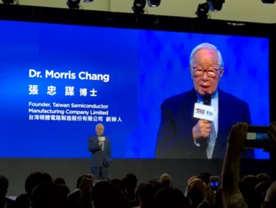
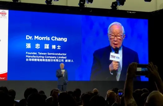
Over the past three decades, most of the world’s innovations have centered largely on business models and involved iterative advances of existing technologies, with none matching the global impact of the top 10 semiconductor industry discoveries and advances, Dr. Morris Chang, founder of TSMC and the IC foundry model, said at SEMICON Taiwan 2018 this week.Few have as clear a perspective on the transformative power of semiconductors as Dr. Chang, founder of TSMC and father of the IC foundry model. Keynoting the IC60 Master Forum celebrating the 60th anniversary of the invention of the integrated circuit (IC), Dr. Chang listed what he considers the 10 key semiconductor industry innovation milestones since 1948:1. Invention of the transistor by Shockley, Bardeen, and Brattain – 19482. Silicon transistor – 19543. Integrated circuit – 19584. Moore’s Law – 19655. MOS technology MOS FET – 1964 Silicon gate – 1967 CMOS – 1970 6. Memory DRAM – 1966 Flash – 1967 7. Outsourced assembly and test (OSAT) – 1960s8. Microprocessor – 19709. VLSI systems design – 1970-1980 IP and design tools – 1980-present 10. Foundry model – 1985 Among the most consequential semiconductor advances may be yet to come, Dr. Chang said, citing innovations including artificial intelligence (AI) and machine learning, new device architectures, Extreme Ultraviolet lithography (EUV), 2.5D/3D packaging, and new materials such as graphene and carbon nanotubes.Dr. Chang argued that because bringing an innovation into production is immensely more expensive than proving a theory in a lab, innovators are not always the ones to implement and benefit from their novel ideas. Today, innovation costs are skyrocketing, driving more consolidation across the supply chain.Michael Droeger is director of marketing at SEMI.
Read More
What’s next for smarter, more connected electronics manufacturing - Part 3 The fast-maturing infrastructure now enabling analysis of exponentially larger data volumes brings the microelectronics industry to an inflection point, where the winning companies will be the first to master the use of this data to solve the industry’s emerging challenges. SEMI expands its coverage of these vital issues with a Smart Manufacturing Pavilion and three days of talks SEMICON West, July 10-12 in San Francisco. While deep learning is starting to be applied to image recognition for wafer inspection, it is also being considered for sequential pattern recognition in order to evaluate equipment parameter traces. The next emerging applications will start to use those learned patterns to predict outcomes, and then use those predictions to automate process control. One early application of deep learning is IC process development. “People don’t think of research and development as the first place to automate, but it’s where applying our digitization and simulation has first had impact,” says David Fried, Coventor vice president of Computational Products. He noted that insertion is easier in the lab than in the fab. Technology at 10nm and beyond is now so complex that companies at the leading edge must use process modeling to understand the effect of process variation on their designs. Learning cycles can now be accelerated during development by simulating 10,000 digital wafers instead of running 25 actual wafers during screening, Fried says. Applying structured analysis and machine learning to the data simplifies optimization across the 500 or more interrelated process steps. Coventor has recently introduced a statistical analysis package that aids the design and analysis of process variation experiments by using large volumes of data from its models. Fried says these models are next being used to accelerate the yield ramp in manufacturing. Digital simulation also could speed development of high-mix, lower value products While digital twins are best known for their use in complex, high value products like jet engines, the simulation technology could also enable the electronic manufacturing services (EMS) sector to reduce the time, cost and risk of developing its high mix of products. “The EMS sector’s use of digital twins will be vital for it to smooth the move of CAD/CAM digital design data for so many different products into manufacturing, and to accelerate validation testing of designs and products by doing more of it in the virtual world,” says Dan Gamota, vice president of Engineering and Technical Services at Jabil. Gamota also highlights the push for traceability from the automotive and healthcare markets, where the digital models could be used to quickly assure that the design was built exactly as specified. “In the past year, traceability has evolved from just ‘nice to have’ to ‘how to achieve,’” he adds. “Companies are expecting it, but aren’t willing to accept the cost and risk of doing it alone. We need the community to discuss realistic implementations, identify the most critical elements and bring together the ecosystem partners to build baseline reference architectures for key digital building blocks. The community also needs to assure the reliable flow of data among the electronic manufacturing segments from semiconductor to OSAT to EMS.” Predictive maintenance and virtual metrology applications could mature in next few years While predictive maintenance initially seemed a likely early application of machine learning in factories, it remains a challenge for the electronics sector. “The difficulty is that it’s not clear where to get the most bang for the buck,” says Tom Ho, president of BISTel America, noting that it may make the most sense to track the failure performance of a single expensive part, like an electrostatic chuck, since predicting the failure performance of a whole complex system like an etcher is much harder. “Collecting enough data from all failure types, including especially the rare events, is difficult unless you have a long history of a lot of tools,” adds Doug Suerich, PEER Group product evangelist. “The gain from collecting performance information from many tools across the industry could be big, but many companies still need to overcome concerns around exposing their IP.” Another big opportunity for prediction is virtual metrology – predicting the wafer outcome from the process or sensor data with enough accuracy to replace the physical metrology. “Virtual metrology is improving, and since metrology can be slow and expensive, any reduction could mean a huge potential savings,” says Suerich. “But it is still seen as too scary for many companies. Two to three years from now, companies will expand the practice from lower risk areas into processes that require more confidence in the results.” Moving beyond prediction to automated control needs digital models Once the results are predicted, the model can be used to control or automatically optimize a process and enable the system to learn by itself, usually by reinforcement learning on a digital model. The model can then independently make adjustments to optimize the manufacturing process. “Automated process development is getting close now. Instead of smart guys turning the knobs, deep learning is automating the smart tuning,” says Suerich, suggesting the industry could see widespread adoption in as little as two to three years. This type of machine learning needs a good digital model, and masses of data for learning. One approach uses human experts to build a physics-based model of the clearly understood parts of the process, then turns to deep machine learning to optimize the lesser-understood variables. The alternative, the data-first approach, runs a computer algorithm to suggest the solution purely from data, without human input, and then relies on the human to evaluate the usefulness of the results. Modeling digital twins of wafers could enable automated process control, chamber matching, and fleet matching, says Fried. If every wafer had its own virtual twin with all the upstream metrology and structural information needed to make equipment control decisions, it could feed forward that information to enable the seamless transition from one step in the process to another based on understanding their complex interrelationships. This could potentially improve uniformity across wafers and equipment, and reduce the need for metrology, he argues. Moving metrology sensors into the chamber will also require model-based algorithms to enable dynamic process control in close to real time, says Fried. These algorithms will be needed to acquire, parse, and process the data at high speed, and then to choose how to adjust the controls. “There will be a model behind collecting and interpreting the metrology data,” he notes. “That’s a really rich vein for improvements in process control.” “The end goal is to collect equipment data in real time, analyze it with AI, and send back controls to optimize manufacturing processes,” Jabil’s Gamota says. “This requires a robust architecture for communication between equipment and consistent formats for data collection and analysis. But the cost and complexity of this heavy lifting is too great for any one company to do alone. We need a consensus-based architecture for ingesting, analyzing and acting on the data.” SEMI tests data transfer protocols, benchmarks best practices SEMI is launching a smart data project to identify the various data transfer protocols needed for inter-company communications. The project will feature a proof-of-concept model in a development fab to produce verifiable results so SEMI can better understand how different approaches meet member needs. SEMI’s smart manufacturing technology communities and the Fab Owners Alliance are also benchmarking current smart manufacturing practices in the microelectronics industry to help SEMI members better understand the path forward and potential return on investment. Speakers over all three days at SEMICON West addressing these issues include Active Layer Parametrics, Applied Materials, Applied Research Photonics, ASML, Bosch Rexroth, Cimetrix, Coventor, ECI Technologies, Edwards Vacuum, Final Phase Systems, GE Digital, Infineon, Jabil, Lam Research, Osaro, Otosense, PEER Group, Qualcomm, Rockwell Automation, Rudolph Technologies, Schneider Electric, Seagate, Siemens, Stanford University, TEL, TIBCO Software. See semiconwest.org. What’s next for smarter, more connected electronics manufacturing - Part 1 What’s next for smarter, more connected electronics manufacturing - Part 2 Paula Doe, SEMI
Read More