downloadGroupGroupnoun_press release_995423_000000 copyGroupnoun_Feed_96767_000000Group 19noun_pictures_1817522_000000Member company iconResource item iconStore item iconGroup 19Group 19noun_Photo_2085192_000000 Copynoun_presentation_2096081_000000Group 19Group Copy 7noun_webinar_692730_000000Path
Skip to main content
Default Banner Image

AI

SEMI has long promoted the industry collaboration that has contributed to the rise of the smart digital world we live in today. A world where data is being generated continuously by systems, gadgets, and sensors around us – often referred to as the Internet of Things (IoT). In our personal lives, most of us have smartphones, smart watches, smart TVs and smart cars, and we live in smart homes and smart cities generating huge amounts of data.In the work world, data and analytics are now influencing almost every industry including healthcare, government, financial services, construction and transportation. This data has the potential to transform our lives and make our world even smarter – if we can communicate and process this data, and use it to come up with actionable recommendations or actions. Artificial Intelligence (AI) and Machine Learning (ML) techniques have generated much excitement precisely because they offer us ways to realize the full value of data by harnessing it and transforming it into active intelligence.Data-intensive technologies are required to store, communicate and analyze data. And it all starts with innovation in microelectronics chips and systems spanning processors, memory, sensors, radios and other devices, presenting a huge opportunity to producers of these technologies. However, with Moore's Law beginning to slow, technology paths and innovation options are diverging. Companies must swiftly assess these options in order to develop competitive offerings. But the technological complexity and divergence makes it increasingly expensive or even unaffordable for many companies to track and pursue these options.The good news is that cost-effective early assessment is possible through pre-competitive collaboration that can produce new and often unexpected cross-disciplinary insights by overcoming traditional silos in industry and academia. Unfortunately, important collaborative industry platforms, such as the International Technology Roadmap for Semiconductors (ITRS), have folded, opening a collaboration gap in the global microelectronics ecosystem.As part of its mission to help companies connect, collaborate, and innovate, SEMI has built a collaborative, cross-supply-chain platform – the Strategic Innovation Platform (SIP). The goal is to provide early and comprehensive assessment of future technologies that are five to eight years away from commercialization. The assessment identifies not just technical barriers but also manufacturing and supply-chain constraints to implementing new technologies. SIP brings together the entire microelectronics ecosystem including strategic technology thought leaders, subject matter experts, technology and application developers, academia, researchers, start-ups and government. With more than 2,100-member companies spread across the global electronics manufacturing supply chain, SEMI is uniquely positioned to enable this critical collaboration. Award-Winning First ProjectThe inaugural SIP project assessed key drivers of future technologies. A key finding was that fast, efficient interconnects between devices and components are critical to the system performance important to customers and users, implying that system-level optimization is required. For data-intensive applications, interconnects have emerged as a key bottleneck for both performance and power in various circuits and systems in part because the slowing of Moore’s Law has decelerated advances in individual device performance, and in part because systems are becoming more complex, requiring heterogeneous integration.To address this challenge, SIP brought together industry experts from ASE Inc., Dow Chemical, Lam Research, Qualcomm and Xilinx to assess the future impact of interconnects for data-intensive applications. SEMI also involved Stanford University professors to collaborate on modeling and simulation. Through this unique cross-disciplinary collaboration, SIP developed a realistic model to evaluate the system-level performance of single-chip systems, as well as multi-chip systems – including traditional 2D packages, high-performance 2.5D systems that use interposers, and futuristic 3D systems. SIP also explored supply chain challenges in business continuity, manufacturability, Environment, Health and Safety (EHS) and the regulatory environment. SEMI worked with a broad range of industry partners to ensure that the model parameters accurately reflected realities on the design and factory floors to ensure usable results. Experimentation has become ever more expensive, with one industry player reporting that “it costs us $100 million to do a good experimental evaluation.” Accurate models can go a long way toward reducing the cost of technology assessment. The SIP collaboration produced key quantifiable insights including comparisons that highlight the benefits and limitations of various materials being explored for future interconnects, and of architectures under consideration for future data-intensive applications. For example, the current workhorse for artificial intelligence (AI) platforms – 2.5D technology – delivers a 4X improvement over 2D packaging but falls short of providing the orders-of-magnitude improvement that future AI/ML applications may require. These findings enable the industry to begin to identify ways to optimize 2.5D architectures, transition to 3D heterogeneous integration for performance-critical applications in the medium term, and to eventually evaluate new paradigms such as neuromorphic and quantum. The project findings were presented late last year in the form of two research papers at Electronics System-Integration Technology Conferences (ESTC) and International Microelectronics Assembly and Packaging Society (IMAPS) recently. One received the “Best Paper of the Session” award at IMAPS – a recognition that affirms the power of a collaborative platform such as SIP to produce valuable insights to address the growing technology complexity within the microelectronics industry. The microelectronics industry is on the cusp of a historic inflection point, where it could fuel the rise of emerging applications in AI/ML and IoT, and can grow into a trillion dollar industry over the next several years. More importantly, the industry is poised to help solve some of society’s most complex problems in areas including healthy living, climate change and transportation. No company can do this alone, and pre-competitive platforms such as SIP are key both to accelerating innovation through cross-disciplinary collaboration, and to reducing costs for individual companies. Please contact Tom Salmon at [email protected] or Pushkar Apte at [email protected] for more details and to get involved in future projects.Tom Salmon is vice president of Collaborative Technology Platforms. Pushkar Apte is a strategic technology advisor at SEMI.
Read More
Artificial intelligence (AI) is on the verge of transforming entire industries as it gears up to power semiconductor industry innovation and growth, thrusting the technology to front and center at SEMICON Japan 2019, December 12-14 at the Tokyo Big Sight (Tokyo International Exhibition Center).The SMART Technology Forum at SEMICON Japan will highlight the latest AI developments and trends. Supported by U.S. Commercial Service in Japan, the forum will feature Yutaka Matsuo of the University of Tokyo. An authority on AI, Matuso will give an overview of both AI business and technology. His presentation will be followed by an AI outlook from Microsoft Japan, Amazon Web Services and DefinedCrowd.A number of Japanese startups are on leading edge of AI innovation in machine and deep learning. One is Preferred Networks Inc., a company that applies cutting-edge deep learning technology to Internet of Things (IoT) applications across transportation, manufacturing and healthcare.In his opening day keynote at SEMICON Japan, Toru Nishikawa, president and CEO of Preferred Networks, Inc., will highlight the latest developments and promise of using deep learning for industrial applications. Nishikawa will unpack how AI companies jockeying for competitive advantage will win by harnessing technologies to process massive amounts of data efficiently and quickly.Following is look at Preferred Networks, Inc. and five other Japanese startups that are driving AI innovation. Within Japan's world of AI, machine learning, and deep dearning, Preferred Networks is likely the most well-known Japanese company. The parent company, Preferred Infrastructure, was founded in March 2006 by Toru Nishikawa and Daisuke Okanohara, who focused on search engine development before turning to machine learning and establishing Preferred Networks to commercialize the technology.Preferred Networks established itself as one of the world’s top providers of machine learning technology with the development of Chainer – an open source deep learning framework that has been offered free of charge since June 2015 and was released before TensorFlow, Google’s renowned Deep Learning framework. Established in 2012, ABEJA is thought to be Japan’s first venture company to specialize in deep learning. ABEJA's core technology is its AI platform ABEJA Platform. Based on this platform, the company offers various solutions to more than 100 client companies. ABEJA also offers ABEJA Insight, a specialized package service for the retail and distribution, manufacturing, and infrastructure industries. Data analytics provider BrainPad Inc. was the first Japanese AI venture listed on the Tokyo Stock Exchange. Established in 2004, before the advent of big data, BrainPad Inc. cultivated a vision of analyzing vast amounts of data in increase the competitiveness of Japanese companies. LeapMind Inc. aims to offer deep learning technology that uses fewer computing resources and draws less power. Both are important capabilities since deep learning requires considerable computing resources to perform image and speech recognition. The company’s answer to this deep learning challenge is a small form factor FPGA with low power consumption.In April 2018, LeapMind started offering the tool DeLTA-Lite to support model construction for Deep Learning. The tool simplifies the development of deep learning design models, eliminating the need for model design, hardware, and software expertise. Hacarus Inc.’s HACARUS-X AI technology, which combines sparse modeling and machine learning technology, features low power consumption and small devices such as FPGAs. In collaboration with semiconductor trading company PALTEK, Hacarus is integrating HACARUS-X algorithms with Xilinx's FPGA Zynq UltraScale + MPSoC. Both companies area also implementing HACARUS-X algorithms in a box computer.Sparse modeling is gaining attention as a modeling method by which humans can understand the judgment process of AI by extracting features from a small amount of learning data. With expertise in life science fields such as medical and biology and image processing technology, LPixel, Inc. develops image analysis systems with original algorithms and machine learning techniques. It has developed a cloud-based AI image analysis platform and an AI medical image diagnosis support technology that streamlines the review of large amounts of research data and detects image fraud in research papers and other documents for the medical and biology fields, freeing researchers to devote more time to their core work. Yoichiro Ando is a marketing director at SEMI Japan.
Read More
Even for someone who has been in this industry since the days of the TI Datamath 4-function calculator and the TMS1100 4-bit microcontroller (yes, that’s been a LONG time – the movie Grease premiered the same year!), it is sometimes hard to grasp the scope and complexity of what happens in today’s leading-edge semiconductor gigafabs. In fact, the only way to comprehend the enormous volume of transactions that occur is to consider what happens in a single minute – this is illustrated in the infographic we have labeled “The Gigafab Minute.”* It’s amazing enough to think that a single factory can start 100,000 wafers every month on their cyclical journey through 1500 process steps… and have 99%+ of them emerge 4 months later to be delivered to packaging houses and then on to waiting customers. It’s quite another to realize that all of this happens continuously (24 x 7) and automatically. “How is this possible?” you ask.Well, a big part of the solution is the body of SEMI standards which have evolved since the early 80s to keep pace with the ever-changing demands of the industry. From an automation standpoint, many of these standards deal with the communications between manufacturing equipment and the factory information and control systems that are essential for managing these complex, hyper-competitive global enterprises.A significant characteristic of these standards is that they have been carefully designed to be “additive.” This means that new generations of SEMI’s communications standards do not supplant or obsolete the previous generations, but rather provide new capabilities in an incremental fashion. To appreciate the importance of this in actual practice, consider how the GEM, GEM300, and EDA/Interface A standards support the transactions that occur in a single Gigafab Minute.Starting at 1:00 o’clock on the infographic and moving clockwise, you first notice that 2.31 wafers enter the line. Of course, these are actually released in 25-wafer 300mm FOUPs (Front-Opening Unified Pod), but 100K wafers per month translates to 2.31 per minute. Since these factories run continuously, once the line is full, it stays full. And with an average total cycle time of 4 months, this means that there are 400K wafers of WIP (work in process) in he factory at any given time. This number, and the total number of equipment (5000+), drive the rest of the calculations.GEM (Generic Equipment Model) – SEMI E30, etc.The GEM messaging standards were initially defined in the early 90s to support the factory scheduling and dispatching applications that decide what lots should go to what equipment, the automated material handling systems that deliver and pick-up material to/from the equipment accordingly, the recipe management systems that ensure each process step is executed properly, and the MES (Manufacturing Execution System) transactions that maintain the fidelity of the factory system’s “digital twin.”Every minute of every day, GEM messages support and chronicle the following activities: 240 process steps are completed (i.e., 240 25-wafer lots are processed), 300 recipes are downloaded along with a set of run-specific adjustable control parameters, and 600 FOUPs are moved from one place to another (equipment, stockers, under-track storage, etc.). For each of these activities, the factory’s MES is notified instantaneously.GEM300 – SEMI E40, E87, E90, E94, E157With the advent of 300mm manufacturing in the mid-to-late 90s, a global team of volunteer system engineers from the leading chip makers defined the GEM300 standards to support fully automated manufacturing operations. Starting at 5:00 o’clock on the infographic, the number of transactions per minute jumps almost 3 orders of magnitude, from the monitoring of 900 control jobs across 4000 process tools to the tracking of 360,000 individual recipe step change events. This level of event granularity is essential for the latest generation of FDC (Fault Detection and Classification) applications, because precise data framing is a key prerequisite for minimizing the false alarm rate while still preventing serious process excursions. In this context, more than 6000 recipe-, product- and chamber-specific fault models may be evaluated every minute.Simultaneously, the applications that monitor instantaneous throughput to prevent “productivity excursions” and identify systemic “wait time waste” situations depend on detailed intra-tool wafer movement events. In a fab with hundreds of multi-chamber, single-wafer processes, 75,000 or more of these events occur every minute. EDA (Equipment Data Acquisition) – SEMI E120, E125, E132, E134, E164, etc.Rounding out the SEMI standards in our example gigafab is the suite of EDA standards which complement the command and control functions of GEM/GEM300 with flexible, high-performance, model-based data collection. The EDA standards enable the on-demand collection of the volume and variety of “big data” required from the equipment to support the advanced analysis, machine learning, and other AI (Artificial Intelligence) applications that are becoming increasingly prevalent in leading semiconductor manufacturers. As EUV (Extreme Ultraviolet) lithography moves from pilot production to high-volume manufacturing at the 7nm process node and beyond, the litho process area will become a major source of process data by itself, generating 10 GB of data every minute. This is in addition to the 100 GB of data collected from other process areas. The End ResultThe final wedge (12:00 o’clock) in our infographic highlights the real objective – which is producing the millions of integrated circuits that fuel our global economy and provide the technologies that are an integral part of our modern way of life. Assuming a nominal die size of 50 square mm (typical of an 8 GB DRAM), the 2.31 wafers we started at 1:00 o’clock result in almost 3200 individual chips. But none of this would be possible without the pervasive factory automation technology we now take for granted. So, as you finish reading this posting on whatever device you happen to be using, take a micro-moment to acknowledge and thank the hundreds of standards volunteers whose insights and efforts made this a reality!You may not be responsible for running a gigafab anytime soon, but the SEMI standards used in this setting are no less applicable to any Smart Manufacturing environment. Give us a call if you’d like to know more about how these technologies can benefit your operations for many years to come.Alan Weber is Vice President, New Product Innovations, at Cimetrix Incorporated. Previously he served on the Board of Directors for eight years before joining the company as a full-time employee in 2011. Alan has been a part of the semiconductor and manufacturing automation industries for over 40 years. He holds bachelor’s and master’s degrees in Electrical Engineering from Rice University. For more information on SEMI Standards, please click here.
Read More
Over the past three decades, most of the world’s innovations have centered largely on business models and involved iterative advances of existing technologies, with none matching the global impact of the top 10 semiconductor industry discoveries and advances, Dr. Morris Chang, founder of TSMC and the IC foundry model, said at SEMICON Taiwan 2018 this week.Few have as clear a perspective on the transformative power of semiconductors as Dr. Chang, founder of TSMC and father of the IC foundry model. Keynoting the IC60 Master Forum celebrating the 60th anniversary of the invention of the integrated circuit (IC), Dr. Chang listed what he considers the 10 key semiconductor industry innovation milestones since 1948:1. Invention of the transistor by Shockley, Bardeen, and Brattain – 19482. Silicon transistor – 19543. Integrated circuit – 19584. Moore’s Law – 19655. MOS technology MOS FET – 1964 Silicon gate – 1967 CMOS – 1970 6. Memory DRAM – 1966 Flash – 1967 7. Outsourced assembly and test (OSAT) – 1960s8. Microprocessor – 19709. VLSI systems design – 1970-1980 IP and design tools – 1980-present 10. Foundry model – 1985 Among the most consequential semiconductor advances may be yet to come, Dr. Chang said, citing innovations including artificial intelligence (AI) and machine learning, new device architectures, Extreme Ultraviolet lithography (EUV), 2.5D/3D packaging, and new materials such as graphene and carbon nanotubes.Dr. Chang argued that because bringing an innovation into production is immensely more expensive than proving a theory in a lab, innovators are not always the ones to implement and benefit from their novel ideas. Today, innovation costs are skyrocketing, driving more consolidation across the supply chain.Michael Droeger is director of marketing at SEMI.
Read More
The march to greater precision, efficiency and safety – the lifeblood of high-technology manufacturing facilities – has taken on a new urgency as emerging applications such artificial intelligence (AI), the Internet of Things (IoT) and Industry 4.0 give new meaning to smart factories. Facing fiercer competition and ever more sophisticated fabrication processes, semiconductor fabs are under intense pressure to keep pace with new technologies as they work to upgrade. Nowhere are the stakes higher than in Taiwan, where high-tech manufacturing contributes mightily to the region’s GDP growth. To help Taiwan fabs confront the challenges and opportunities of designing smarter factories, SEMI and its High-Tech Facility Committee hosted the High-Tech Facility Workshop in June. SEMICON Taiwan 2018 High-Tech Facility Pavilion exhibitors gathered to explore how they can build smarter factories by deploying smart surveillance and disaster prevention technologies along with smart communications systems that better use manufacturing data to drive new safety and product quality efficiencies.During the workshop, SEMI High-Tech Facility Committee representatives shared strides it has made upgrading overseas facilities and developing standards to help establish smart factories in Taiwan.SEMICON Taiwan – 5-7 September at Taipei’s Nangang Exhibition Center – is also an important event for advancing smart manufacturing in Taiwan. Nearly 30 leading global manufacturers will exhibit at the SEMICON Taiwan High-Tech Facility Pavilion. The venue covers operational aspects of semiconductor manufacturing vital to becoming smarter including energy savings, nano-contamination control, facility information modeling, precision instrumentation and control, fire protection, mechatronics, and automation control. The pavilion will also feature a series of theme events offering a comprehensive overview of topics including the latest practices for integrating smart facility capabilities from the perspective of an advanced fab designer.At the TechXPOT stage, High-Tech Facility Pavilion exhibitors will also demonstrate the latest technology breakthroughs and cutting-edge smart factor solutions.The September 6th High-Tech Facility International Forum at SEMICON Taiwan will again gather factory experts and thought leaders from industry and academia to examine “Effective Ways to Make a Facility Smart.“ Experts from industry heavyweights in the fields of wafer foundry, LCD, memory and semiconductor packaging including TSMC, UMC, Innolux, ASE, Micron Taiwan, Winbond and VIS will offer insights into key areas of high-tech facilities including facility electricity, machinery, water management, vaporization and automation systems. On the same day as the forum, the High-Tech Facility Get-Together and High-Tech Facility VIP Dinner will bring together industry elites, academic professionals, and government officials to explore partnership opportunities. SEMI Taiwan and the High-Tech Facility Committee share HTF market trends information, technology updates and standards with SEMI members and exhibitors. Founded in 2013, the High-Tech Facility Committee now has 85 corporate members. Dedicated to accelerating industry collaboration through the integration of Taiwan industrial, government and academic resources, the committee each year holds several group meetings focusing on topics including energy savings, earthquake and fire protection, nano-contamination control, and precision instrumentation and control to advance critical technologies and facilitate standardization. The committee also aims to help the industry become more competitive faster by promoting technology standards that boost productivity and reduce production costs.Please visit www.semi.org and www.semicontaiwan.org for more information about SEMI’s high-tech facility initiatives.Iris Tsou is a marketing specialist at SEMI Taiwan.
Read More
With artificial intelligence (AI) rapidly evolving, look for applications like voice recognition and image recognition to get more efficient, more affordable, and far more common in a variety of products over the next few years. This growth in applications will drive demand for new architectures that deliver the higher performance and lower power consumption required for widespread AI adoption. “The challenge for AI at the edge is to optimize the whole system-on-a-chip architecture and its components, all the way to semiconductor technology IP blocks, to process complex AI workloads quickly and at low power,” says Qualcomm Technologies Senior Director of Engineering Evgeni Gousev, who will provide an update on the progress of AI at the edge in a Data and AI program at SEMICON West, July 10-12 in San Francisco. Qualcomm Snapdragon 845 uses heterogeneous computing across the CPU, GPU, and DSP for power-efficient processing for constantly evolving AI models. Source: QualcommA system approach that optimizes across hardware, software, and algorithms is necessary to deliver the ultra-low power – to a sub 1-milliwatt level, low enough to enable always-on machine vision processing – for the usually energy-intensive AI computing. From the chip architecture perspective, processing AI workloads with the most appropriate engine, such as the CPU, GPU, and DSP with dedicated hardware acceleration, provides the best power efficiency – and flexibility for dealing with rapidly changing AI models and growing diversity of applications.“So far it’s been largely a brute force approach using conventional architectures and cloud-based infrastructure,” says Evgeni. “But we’re going to run out of brute force options, so future opportunities lie in developing innovative architectures, dedicated hardware, new algorithms, and new software. Innovation will be especially important for AI at the edge and applications requiring always-on functionality. Training is mostly in the cloud now, but in the near future it will start migrating to the device as the algorithms and hardware improve. AI at the edge will also remove some privacy concerns, an increasingly important issue for data collection and management.”Practical AI applications at the edge where resources are constrained run the gamut, spanning smartphones, drones, autonomous vehicles, virtual reality, augmented reality and smart home solutions such as connected cameras. “More AI on the edge will create a huge opportunity for the whole ecosystem – chip designers, semiconductor and device manufacturers, applications developers, and data and service providers. And it’s going to make a significant impact on the way we work, live, and interact with the world around us,” Evgeni said.Future generations of chips may need more disruptive systems-level change to handle high data volumes with low power A next-generation solution for handling the massive proliferation of AI data could be a nanotechnology system, such as the collaborative N3XT (Nano-Engineered Computing Systems Technology) project, led by H.S. Philip Wong and Subhasish Mitra at Stanford. “Even with next-generation scaling of transistors and new memory chips, the bottlenecks in moving data in and out of memory for processing will remain,” says Mitra, another speaker in the SEMICON West program. “The true benefits of nanotechnology will only come from new architectures enabled by nanosystems. One thing we are certain of is that massively more capable and more energy-efficient systems will be necessary for almost any future application, so we will need to think about system-level improvements.” Major improvement in handling high volumes of data with low high energy use will require system-level improvements, such as monolithic 3D integration of carbon nanotube transistors in the multi-campus N3XT chip research effort. Source: Stanford UniversityThat means carbon nanotube transistors for logic, high density non-volatile MRAM and ReRAM for memory, fine-grained monolithic 3D for integration, new architectures for computation immersed in memory, and new materials for heat removal. “The N3XT approach is key for the 1000X energy efficiency needed,” says Mitra.Researchers have demonstrated improvements in all these areas, including multiple hardware nanosystem prototypes targeting AI applications. The researchers have transferred multiple layers of as-grown carbon nanotubes to the target wafer to significantly improve CNT density and have also developed a low-power TiN/HfOx/Pt ReRAM. The low-temperature CNT and ReRAM processes enable multiple vertical layers to be grown on top of one another for ultra-dense and fine-grained monolithic 3D integration. Other speakers at the Data and AI TechXpot include Fram Akiki, VP Electronics, Siemens; Hariharan Ananthanarayanan, motion planning engineer, Osaro; and David Haynes, Sr. director, strategic marketing, Lam Research. See SEMICONWest.org.Paula Doe, SEMI
Read More
As artificial intelligence’s (AI) sprawling influence reshapes industries from logistics and healthcare to automotive and manufacturing, Taiwan is poised to leverage its cutting-edge capabilities and rich history in semiconductor manufacturing to stake out a leadership position in AI. Taiwan’s semiconductor manufacturing industry accounts for a major share of the region’s GDP and, with its manufacturing prowess, the region is fertile ground for using AI to optimize and even revolutionize chip manufacturing. In an AI and Semiconductor Smart Manufacturing Forum recently hosted by SEMI Taiwan, experts from Micronix, Advantech, Nvidia and the Ministry of Science and Technology of Taiwan (MOST) shared their insights on how deep learning, data analytics and edge computing will shape the future of semiconductor manufacturing. Here are four key takeaways.1. Monitor, Forecast, and PreventToday, tier 1 foundries use AI tools to combine equipment know-how and manufacturing statistics in managing massive Fault Detection (FD) data, much in the way that a car’s tire-pressure monitoring system helps maintain safe inflation levels and prevent accidents. For example, AI enables the real-time collection and monitoring of massive amounts of processing data, then alerts system administrators of any hardware failures or other manufacturing abnormalities.AI also makes it possible to adopt Run-to-Run (R2R) control to automate manufacturing process adjustments and corrections by providing feedback that can drive higher processing efficiency. In addition, virtual metrology replaces manual sampling inspection for comprehensive quality control, enabling foundries to improve yields, reduce costs, and strengthen their competitive advantage.2. Beyond Automation: Edge Computing The evolution of IoT is giving rise to a paradigm shift in the industry as the recognition grows that smart factories must go beyond automation to focus also on intelligence. All information – from equipment status and manufacturing process statistics to on-site environmental data – needs to be collected through sensors. In highly time-critical scenarios, returning all sensor data to the cloud for processing is time-consuming and impracticable. This is where edge computing’s real-time features and lower cost than cloud computing come into play.How does edge computing work in a smart factory? First, a rich trove of data from various devices is collected and integrated via Manufacturing Execution Systems (MES). Software analysis then produces a real-time factory production status before production data is visualized through a combination of system platforms and human-machine interfaces. In the end, the data is analyzed realtime in the cloud so failures can be predicted and prevented to help increase capacity and reduce costs. The approach is even capable of Bill of Materials (BOM) predictions, allowing better collaboration between upstream and downstream suppliers.3. Deep Learning Accelerates AI Deep learning enables autonomous driving, intelligent voice assistance and many other AI breakthroughs. The heart of deep learning is its ability to automatically process and learn data in various formats such as images, video and text with no human domain knowledge. This increases predictive accuracy and efficiency in processing massive amounts of data. Deep learning also enhances the efficiency of human-machine collaboration.4. Taiwan’s Competitive Niche: Industry 3.5Industry 4.0 is not just about improving production management. It also focuses on integrating supply chains, even among competitive companies. For Industry 4.0 to thrive, rival companies must grow together. The first and third industrial revolutions centered on disruptive technologies like steam engines, transistors and digital, while the second and fourth revolutions homed in on competition among various business models, platforms and industry ecosystems.While Taiwan’s strengths include innovation, short time-to-market, low manufacturing costs, and high supply chain management efficiency, the region still lags advanced countries in basic industry and research capabilities. Squeezed by Chinese supply chains and high-end manufacturers in advanced countries, Taiwan should start by carving out an Industry 3.5 niche for the island’s manufacturers. SEMI will continue to facilitate cross-industry connection, collaboration and innovation to help manufacturers seeking higher production efficiency and lower costs incorporate AI as a core competitive advantage. At SEMICON Taiwan 2018, SEMI will unveil its Smart Manufacturing Journey, an exhibition that gathers leading AI companies such as ABB, Advantech, Nvidia, Sony and UPS to demonstrate a comprehensive roadmap for smart manufacturing technologies and applications. For more information, please visit the SEMICON Taiwan website.Emmy Yi is a marketing specialist at SEMI Taiwan.
Read More
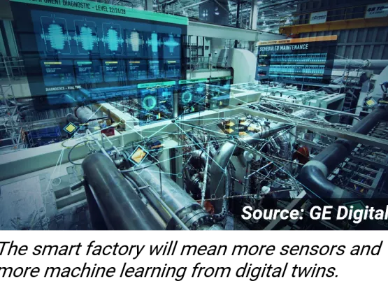
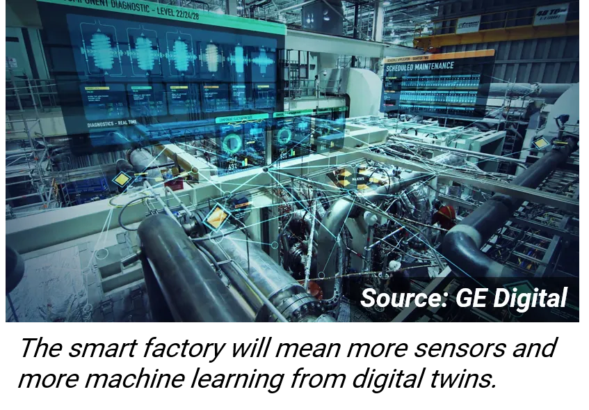
The fast-growing automotive semiconductor market means big change for the IC supply chain. Beyond the obvious demands for reliability and traceability, the sector is moving towards simpler and lower-cost solutions while facing the daunting challenge of automating driving in a complex world. The need for simpler and cheaper automotive intelligence will likely drive acquisitions to build complete platform solutions that are easier to integrate. This demand has already spawned a market for pre-configured test cars to save developers time and money, and is driving LiDAR (Light Detection And RADAR) towards lower-cost, solid state solutions. “The growth of the automotive electronics market provides a great opportunity for the IC supply chain to differentiate on specialty processes and quality for the high-volume automotive business with its long design cycles,” says Scott Jones, principal, strategy, at KPMG, who will speak in the automotive program at SEMICON West. “This differentiation is a chance to reduce chip suppliers’ dependence on scaling volume for the mobile phone world with its short-cycle volatility of winning and losing sockets.” He notes that increasing demand for automotive ICs is also reinvigorating the eight-inch supply chain and spurring opportunity for specialty products such as compound semiconductor devices for power efficiency. Supplying the automotive market also means addressing automotive reliability requirements, which can be 10 times more stringent than for consumer devices. At the same time, the industry must sustain fast-paced development cycles required for the volume and diversity of low-cost IoT devices, manage the segmented supply chain for both those markets, and still spread development costs. Another big challenge for the supply chain will be to automate testing and update vast amounts of embedded software in these automotive devices. “The more complete solution a company can put together, the more the automakers will gravitate to it. They want simplicity,” Jones suggests. Smaller players will need to differentiate with IP and acquire other IP provider to build a broader platform, or be acquired and folded into an all-in-one solution.AutonomouStuff helps accelerate and simplify development of autonomous driving solutionsAutonomouStuff is helping to speed development of these platforms. The company has grown from a sensor distributor into a supplier in the emerging niche of vehicles preconfigured with key interfaces for sensors and controls. These interfaces can then be customized by integrating different components for developers to test their applications. AutonomouStuff offers developers a lineup of vehicle models pre-configured with the interfaces needed to add desired chips, sensors and software to develop their autonomous vehicle systems. Source: AutonomouStuff.“Whether they’re major chipmakers or AI software startups, they don’t have a year to build their own vehicle platforms themselves for developing autonomous vehicle systems,” says Wolfgang Juchmann, VP sales and business development at AutonomouStuff. Juchmann, a SEMICON West speaker, will bring a demonstration vehicle to the show. “In four to six weeks we can prepare a custom test car with selected sensors, enabling users to start testing their computer platforms and software. It’s faster and more cost-effective for us to supply the car with the needed interfaces.” He notes that developers are using some 300 AutonomouStuff vehicles in the field. AutonomouStuff customers are starting to transition from testing on a single car or two to testing on mini-fleets with 50 to 100 vehicles. Beyond sensors and pre-configured vehicles, the next step will be to add more data intelligence services to help with capabilities like tagging the data for training, Juchmann says. AutonomouStuff already offers hardware to support Baidu’s Apollo open-source software stack and data set. The company was recently acquired by the Swedish holding company Hexagon to help support expansion.CMOS silicon LiDAR nears automotive qualificationInnovations in the hyper-competitive LiDAR market, where burgeoning demand is driving the race to develop various types of solid-state devices, may also help reduce the cost of autonomous vehicles. Among the roughly 40 LiDAR suppliers, at least one – Quanergy – is taking advantage of 45nm and 32nm foundry CMOS volume production. The company uses voltage through the semiconductor stack to change the refractive index, controlling the phases of optical beams and the resulting interference patterns of light exiting the chip to quickly steer the laser beam without the need for moving parts, much like the phased array radar its team developed earlier. Solid state LiDAR image with object recognition software. Source: QuanergySo far, most of the small LiDAR units have shipped to the security, industrial automation, drone, robots and 3D mapping markets. However, Quanergy CEO Louay Eldada, another SEMICON speaker, says the company is also winning automotive designs and expects automotive shipments to take off early next year, once automotive certification testing is completed. “We can get design wins because standard CMOS production at TSMC makes us a known entity,” says Eldada. To prevent component misalignment, the company produces its own specialized packaging to secure the laser, phase control ASIC, optical phased-array emitter, detector array, and receiver readout ASIC at its plant in Silicon Valley or the facility of its automotive partner Sensata. Through its software business, Quanergy offers an artificial intelligence (AI) perception program for object recognition and LiDAR tracking. The solution uses the people-tracker software the company acquired from Raytheon.SEMICON West this year expands to three full days of automotive electronics programming and features a Smart Transportation Pavilion. Other companies with experts who will speak as part of the program include XPT/NIO, Infineon, McKinsey, Voyage, GM Cruise, Bosch, Deepen AI, Airbus A3, Nvidia, Excelfore, Byton, Macronix, SK Hynix, SAP, Xilinx, Achronics, California Fuel Cell Partnership, Velodyne, Lam Research, KLA-Tencor, SCREEN, Rockwell, Versum Materials, TechSearch International, Entegris, ASE, Amazon, Continental and Wind River. www.semiconwest.orgPaul Doe, SEMI
Read More
The fast-maturing hardware and software that are enabling practical applications of equipment intelligence and machine learning mean disruptive change for microelectronics manufacturing. But first comes the basic work of building the basic infrastructure, figuring out IP separation, and learning to solve physical problems in the digital world. Just how much can the semiconductor industry leverage industrial IoT practices from other industries? Common wisdom may be that industrial software solutions aren’t well suited to the IC sector’s complex needs. But GE Digital enterprise account executive Luke Smaul, currently working with Intel, argues that semiconductor fabs and toolmakers are dealing with similar issues as GE did when it first started working with Delta Airlines to monitor the GE engines on Delta planes. Smaul will speak at SEMICON West about GE’s work with Intel over the past few years and, in particular, how its solution for cloud security and IP separation can work for ICs. “GE learned to provide IP security and separation in the aviation space with its suppliers, which moved us all up the value chain, providing a big engine for growth,” says Smaul, who started his career as an IC engineer. “GE Aviation saw a 25 percent increase in issue detection rates by leveraging the same common platform. We’ve shown that we can protect Intel intellectual property in its own cloud space and control who can access what.” A toolmaker can access only particular fab data as needed for analysis, and then can reveal only the output from the analysis and a subset of supporting data. “IP separation has to happen, and it will unlock huge added value,” Smaul says. GE’s Predix solution aims to supply an easy-to-use, plug-and-play system for analytics to enable a yield engineer without a deep data background to select a supported sensor, a gateway to connect automatically to the cloud, and an analytics application to test a hypothesis of how the collected data relates to yield. “This empowers the yield engineer to use and unlock information for a quick improvement, even for simple things such as looking at the impact of degradation of fan performance over time on yield,” says Smaul. “Though the scope may be small, the impact on yield in aggregate, and when scaled, is large.” “There needs to be much more collaboration across the industry to make this work, and to share best practices,” says Smaul. “Just as GE moved from selling gas turbines to selling power-as-a-service, vendors of other big, expensive assets like IC equipment will likely change their business model from selling tools towards selling yield-as-a-service. This will simplify life for the fab while bringing the toolmaker more opportunity to sell improved capabilities on existing tools.” More human intelligence makes AI smarter Applying AI neural network approaches such as deep learning to predict outcomes from digital models is enabling disruptive advances in speech and image recognition, but applying it to complex IC manufacturing problems such as predictive maintenance has been a challenge. These neural networks require massive amounts of data to train, and the IC sector doesn’t really have big data, just a lot of little data clusters due to the dynamics and context richness of processes. This data is difficult to combine for analysis. In addition, the neural network provides only an answer but can’t explain why, notes Michael Armacost, managing director of advanced service engineering at Applied Materials. “We’ve learned that it works better if we do not ignore what we know already, but rather incorporate expert knowledge in a structured way to help us focus on the key features and the key data,” says Armacost, who will also speak in the program. This includes choosing the most important steps to include in the model, identifying the limited data to collect and how to filter the data for outliers, and then selecting the final parameters and features, adjusting the limits, and making adjustments as results drift change over time. The less data needed, the better for the complicated issue of IP protection as well. The big gains from these new analysis approaches will likely require data from more than one company and supporting security for remote connectivity. “Some end users are attempting to do the AI all themselves, but in the long term there will need to be collaboration across companies,” says James Moyne, University of Michigan professor and consultant to Applied Materials, another speaker. Collaboration will need to balance the value of the solution against the risk of compromising IP. “The low-hanging fruit are applications such as predictive maintenance in areas that do not involve high-priority IP. Another approach will be to limit the amount of shared data needed – to first build the model on a wide range of data, but then to use only a very small amount of data to operate the models.” Ready-made models could speed the process Coventor’s semiconductor process models are finding initial applications in R D whereby companies use the simulation to understand the effect of process variation on their complex designs. Instead of running dozens of actual wafers to optimize semiconductor processes, users can instead quickly simulate the results of complex process interactions on their design. Going forward, the process models could find a wide range of applications, from accelerating stabilization of new processes in the fab to enabling real-time co-optimized control across previously independent unit steps to improve wafer uniformity. “This improved uniformity across wafers and equipment could potentially reduce the need for costly physical silicon validation,” suggests Joseph Ervin, Coventor director, semiconductor process and integration, another SEMICON speaker. “Making use of in-situ metrology for real-time control also demands a digital model to process and analyze the collected data for quick response. This area has tremendous potential for improving semiconductor process control.” SEMICON West features a Smart Manufacturing Pavilion with displays and three full days of speakers on building the infrastructure needed to enable disruptive artificial intelligence in the microelectronics sector. www.semiconwest.org The SEMICON West Smart Manufacturing Pavilion features interactive Touch Liquid Crystal Displays (TLCD) and working production equipment on the floor from Bosch Rexroth, Cimetrix, Rudolph Technologies, Inficon/Final Phase Systems, OMRON, DISCO and Edwards Vacuum. For information on the SEMI Smart Manufacturing Initiative and how to get involved, please click here. Paula Doe, SEMI
Read More