downloadGroupGroupnoun_press release_995423_000000 copyGroupnoun_Feed_96767_000000Group 19noun_pictures_1817522_000000Member company iconResource item iconStore item iconGroup 19Group 19noun_Photo_2085192_000000 Copynoun_presentation_2096081_000000Group 19Group Copy 7noun_webinar_692730_000000Path
Skip to main content

MILPITAS, Calif. ─ April 16, 2024 ─ SEMI, the industry association serving the global electronics design and manufacturing supply chain, today applauded the United States Department of Commerce’s announcement of a Preliminary Memorandum of Terms for an award under the CHIPS and Science Act to support the expansion of Samsung Electronics’ presence in Texas and the company’s development and production of leading-edge chips. The award includes $6.4 billion in grants and an investment tax credit to help fund two new leading-edge logic fabs, a research and development fab, and an advanced packaging facility in Taylor, Texas. Samsung Electronics will also use the funding to expand its Austin fabs.

“SEMI applauds the U.S. Department of Commerce for this latest step to enhance the resilience of the domestic semiconductor supply chain and supply of advanced chips,” said Joe Stockunas, President of SEMI Americas. “The CHIPS and Science Act investment will enable Samsung Electronics to grow its manufacturing footprint in Texas while supporting the buildout of an ecosystem with advanced packaging and R&D capabilities.”

“With Samsung expected to invest more than $40 billion in the region in the coming years, this proposed CHIPS investment would strengthen the standing of Central Texas as a leading-edge semiconductor ecosystem, creating more than 4,500 good-paying manufacturing jobs and 17,000 construction jobs,” Stockunas said.

Visit SEMI Global Advocacy to learn more about public policy efforts and developments, and SEMI Workforce Development for more information on efforts to address the microelectronics industry’s talent needs.

About SEMI
SEMI® is the global industry association connecting over 3,000 member companies and 1.5 million professionals worldwide across the semiconductor and electronics design and manufacturing supply chain. We accelerate member collaboration on solutions to top industry challenges through Advocacy, Workforce Development, Sustainability, Supply Chain Management and other programs. Our SEMICON® expositions and events, technology communities, standards and market intelligence help advance our members’ business growth and innovations in design, devices, equipment, materials, services and software, enabling smarter, faster, more secure electronics. Visit www.semi.org, contact a regional office, and connect with SEMI on LinkedIn and X to learn more.

Association Contacts

Samer Bahou/SEMI US
Phone: 1.408.943.7870
Email: [email protected]

Michael Hall/SEMI
Phone: 1.408.943.7988
Email: [email protected]

MILPITAS, Calif. ─ April 8, 2024 ─ SEMI, the industry association serving the global electronics design and manufacturing supply chain, today applauded the United States Department of Commerce’s announcement of a Preliminary Memorandum of Terms for an award under the CHIPS and Science Act to support the construction of Taiwan Semiconductor Manufacturing Company (TSMC) chip manufacturing facilities in Arizona. The award includes $6.6 billion grants, as much as $5 billion in loans and an investment tax credit.

“We applaud the U.S. Department of Commerce for taking this significant step to enhance the resilience of the domestic semiconductor supply chain,” said Joe Stockunas, President of SEMI Americas. “This CHIPS and Science Act award is a key stride towards a 2-nanometer process, positioning the United States to produce the most advanced semiconductor chips at scale in order to advance global supply chain stability and help meet worldwide chip demand across various markets.”

“This grant increases TSMC's total investment in Arizona to $65 billion and is expected to create 6,000 direct jobs, 20,000 construction jobs and thousands of supporting ecosystem jobs, further demonstrating the positive economic impact and job creation potential of such advancements in semiconductor manufacturing,” Stockunas said.“Government investments like the CHIPS and Science Act grant for TSMC play a crucial role in semiconductor manufacturing and are of immense importance to economies globally.”

The recently announced SEMI 300mm Fab Outlook to 2027 report projects the Americas region will double 300mm fab equipment investments from US$12 billion in 2024 to US$24.7 billion in 2027, significantly narrowing the gap with the top three spending regions, which are projected to invest between US$26.3 billion and US$30 billion in chipmaking equipment in 2027.

Visit SEMI Global Advocacy to learn more about public policy efforts and developments, and SEMI Workforce Development for more information on efforts to address the microelectronics industry’s talent needs.

About SEMI
SEMI® is the global industry association connecting over 3,000 member companies and 1.5 million professionals worldwide across the semiconductor and electronics design and manufacturing supply chain. We accelerate member collaboration on solutions to top industry challenges through Advocacy, Workforce Development, Sustainability, Supply Chain Management and other programs. Our SEMICON® expositions and events, technology communities, standards and market intelligence help advance our members’ business growth and innovations in design, devices, equipment, materials, services and software, enabling smarter, faster, more secure electronics. Visit www.semi.org, contact a regional office, and connect with SEMI on LinkedIn and X to learn more.

Association Contacts

Samer Bahou/SEMI US
Phone: 1.408.943.7870
Email: [email protected]

Michael Hall/SEMI
Phone: 1.408.943.7988
Email: [email protected]

MILPITAS, Calif. – April 10, 2024 – Worldwide sales of semiconductor manufacturing equipment edged down 1.3% to $106.3 billion in 2023 from an all-time record of $107.6 billion in 2022, SEMI, the industry association representing the global electronics design and manufacturing supply chain, reported today. The data is now available in the Worldwide Semiconductor Equipment Market Statistics (WWSEMS) report.

China, Korea and Taiwan – the top three regions in chip equipment spending in 2023 – accounted for 72% of the global equipment market, with China remaining the largest semiconductor equipment market. The pace of investments in China accelerated 29% year-over-year, reaching $36.6 billion in billings last year. Equipment spending in Korea, the second-largest equipment market, fell 7% to $19.9 billion on softer demand and the memory market inventory correction. After posting four straight years of growth, equipment sales to Taiwan also contracted 27% to $19.6 billion.

Annual semiconductor equipment investments in North America rose 15%, largely on the strength of CHIPS and Science Act investments, while Europe logged a 3% increase. Sales to Japan and the Rest of World decreased 5% and 39% year-over-year, respectively.

“Despite a slight dip in global equipment sales, the semiconductor industry continues to show strength, with strategic investments fueling growths in key regions,” said Ajit Manocha, SEMI President and CEO. “The overall results for the year were better than anticipated by most industry followers.”

Global sales of wafer processing equipment rose 1% in 2023, while other front-end segment billings grew 10%. After contracting in 2022, assembly and packaging equipment sales extended their decline, decreasing 30% in 2023, while total test equipment billings contracted 17% year-over-year.

Compiled from data submitted by members of SEMI and the Semiconductor Equipment Association of Japan (SEAJ), the WWSEMS report is a summary of the monthly billings figures for the global semiconductor equipment industry. 


Annual Billings by Region in Billions of U.S. Dollars with Year-Over-Year Change Rates 


The SEMI Equipment Market Data Subscription (EMDS) provides comprehensive market data for the global semiconductor equipment market. The subscription includes three reports:

  • Monthly SEMI Billings Report, a perspective on equipment market trends
  • Monthly Worldwide Semiconductor Equipment Market Statistics (WWSEMS), a detailed report of semiconductor equipment billings for seven regions and 24 market segments
  • SEMI Semiconductor Equipment Forecast, an outlook for the semiconductor equipment market

Download a sample of the EMDS report.

For more information about the report or to subscribe, please contact the SEMI Market Intelligence Team at [email protected]. More details are also available on the SEMI Market Data webpage.

About SEMI
SEMI® is the global industry association connecting over 3,000 member companies and 1.5 million professionals worldwide across the semiconductor and electronics design and manufacturing supply chain. We accelerate member collaboration on solutions to top industry challenges through Advocacy, Workforce Development, Sustainability, Supply Chain Management and other programs. Our SEMICON® expositions and events, technology communities, standards and market intelligence help advance our members’ business growth and innovations in design, devices, equipment, materials, services and software, enabling smarter, faster, more secure electronics. Visit www.semi.org, contact a regional office, and connect with SEMI on LinkedIn and X to learn more.

Association Contact
Michael Hall/SEMI
Phone: 1.408.943.7988
Email: [email protected]

MILPITAS, Calif. ─ April 11, 2024 ─ SEMI, the industry association serving the global electronics design and manufacturing supply chain, today issued the following statement from Ajit Manocha, SEMI President and CEO, after the United States government announced it will no longer move forward with the Notice of Funding Opportunity for CHIPS funding for the construction, modernization, or expansion of semiconductor research and development (R&D) facilities in the United States:

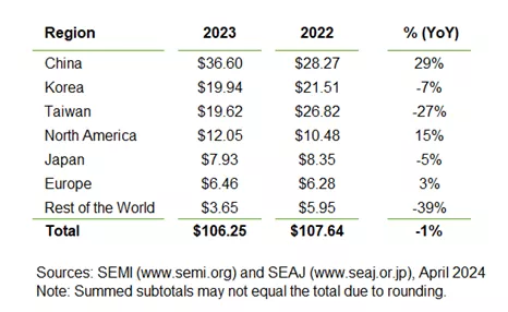
“We recognize that the Department of Commerce was faced with a difficult decision to change course regarding the issuance of a third Notice of Funding Opportunity related to R&D under the CHIPS and Science Act due to recent legislative actions directing the department to make a $3.5 billion investment in secure enclave. While we acknowledge the importance of the underlying objectives guiding recent decisions, we are concerned about their impact on longstanding plans for implementing the CHIPS Act, which was shaped by extensive stakeholder input and industry analysis.”

“Strong investment and support for R&D is essential to advance foundational technologies across the semiconductor supply chain and enhance the overall competitiveness of the U.S. semiconductor industry. Private R&D is the cornerstone of the semiconductor industry, propelling the next generation of innovation. SEMI urges Congress to work alongside the Department of Commerce to fulfill the intent of the CHIPS and Science Act of 2022 to fund private R&D activities under the legislation. Key investments to spur and scale private R&D projects must be paired with support for the National Semiconductor Technology Center (NSTC) to meet the objectives of CHIPS and Science Act and secure the United States’ technological leadership. SEMI stands ready to work with the Department of Commerce and Congress to ensure robust funding for private R&D projects.”

Visit SEMI Global Advocacy to learn more about public policy efforts and developments, and SEMI Workforce Development for more information on efforts to address the microelectronics industry’s talent needs.

About SEMI
SEMI® is the global industry association connecting over 3,000 member companies and 1.5 million professionals worldwide across the semiconductor and electronics design and manufacturing supply chain. We accelerate member collaboration on solutions to top industry challenges through Advocacy, Workforce Development, Sustainability, Supply Chain Management and other programs. Our SEMICON® expositions and events, technology communities, standards and market intelligence help advance our members’ business growth and innovations in design, devices, equipment, materials, services and software, enabling smarter, faster, more secure electronics. Visit www.semi.org, contact a regional office, and connect with SEMI on LinkedIn and X to learn more.

Association Contacts

Samer Bahou/SEMI US
Phone: 1.408.943.7870
Email: [email protected]

Michael Hall/SEMI
Phone: 1.408.943.7988
Email: [email protected]

MILPITAS, Calif. — April 9, 2024 — Aiming to help the global semiconductor workforce expand its skills to address the talent gap, SEMI today announced the expansion of the SEMI University™ learning platform to include in-person trainings. Complementing SEMI U online courses, the semiconductor curriculum is designed for technicians, engineers and non-technical staff ranging from new hires to experienced workers looking to advance their careers. The courses cover subjects including front-end and back-end manufacturing operations, principles of chip design, and rapidly evolving technologies such as artificial intelligence (AI), MEMS and advanced packaging.

The initial in-person trainings will be held at SEMI headquarters in Milpitas, California. See the SEMI University Course Calendar for upcoming sessions. SEMI U will also offer instructor-led trainings on July 8, 2024, at the Moscone Center in San Francisco preceding SEMICON West 2024, July 9-11. Discounted SEMI U: Pre-Show Training sessions are available for SEMICON West attendees and students.

“SEMI member companies have flagged the semiconductor industry talent and skills gap as a top concern that could impact long-term growth,” said SEMI University Director Naresh Naik. “Our new SEMI U in-person trainings bolster our online courses in supporting industry efforts to train and upskill employees and help incoming talent establish their careers in pursuing growth. We carefully curated each course topic based on industry demand, emerging trends, and feedback from our existing online courses. By focusing on these specific areas, we aim to address the most pressing needs of our audience, providing them with practical skills and knowledge that are directly applicable to their roles and career advancement.”

SEMI U in-person course topics include:

About SEMI University and the SEMI Workforce Development Program

The SEMI University learning platform offers more than 575 online courses specifically created for the semiconductor industry, providing an easy-to-use online training program in multiple languages for employees ranging from recently hired facility operators to experienced technicians, engineers and non-technical staff.

SEMI has offered in-person training and technology trend updates more than 50 years, and it hosts webinars covering SEMI standards, market dynamics and semiconductor manufacturing and design best practices. SEMI University builds on this experience and adds to the association’s holistic Workforce Development program offered by the SEMI Foundation. The non-profit arm of SEMI, the SEMI Foundation drives initiatives to increase awareness of semiconductor industry careers, connect member companies with university students for mentoring and internships, attract and train military veterans, and develop a more diverse and inclusive workforce.

About SEMI
SEMI® is the global industry association connecting over 3,000 member companies and 1.5 million professionals worldwide across the semiconductor and electronics design and manufacturing supply chain. We accelerate member collaboration on solutions to top industry challenges through Advocacy, Workforce Development, Sustainability, Supply Chain Management and other programs. Our SEMICON® expositions and events, technology communities, standards and market intelligence help advance our members’ business growth and innovations in design, devices, equipment, materials, services and software, enabling smarter, faster, more secure electronics. Visit www.semi.org, contact a regional office, and connect with SEMI on LinkedIn and X to learn more.

Association Contact

Michael Hall/SEMI US
Phone: 1.408.943.7988
Email: [email protected]

MILPITAS, Calif. April 8, 2024 — Electronic System Design (ESD) industry revenue increased 14% to $4,423 million in the fourth quarter of 2023 from the $3,879.9 million logged in the third quarter of 2023, the ESD Alliance, a SEMI Technology Community, announced today in its latest Electronic Design Market Data (EDMD) report. The four-quarter moving average, which compares the most recent four quarters to the prior four, rose 14.1%.

“Electronic design automation (EDA) continued to report strong revenue growth in Q4 2023,” said Walden C. Rhines, Executive Sponsor of the SEMI Electronic Design Market Data report. “The Computer-Aided Engineering, Printed Circuit Board and Multi-Chip Module, Semiconductor Intellectual Property, and Services categories reported double-digit growth. Further, all geographic regions reported substantial growth.”

The companies tracked in the EDMD report employed 60,106 people globally in Q4 2023, an 8.9% jump over the Q4 2022 headcount of 55,192 and up 0.6% compared to Q3 2023.

The quarterly EDMD report contains detailed revenue information with the following category and geographic breakdowns.

Revenue by Product and Application Category – Year-Over-Year Change

  • Computer-Aided Engineering (CAE) revenue increased 19.5% to $1,512.1 million. The four-quarter CAE moving average increased 19.3%.
  • IC Physical Design and Verification revenue declined 1% to $691.5 million. The four-quarter moving average for the category increased 20%.
  • Printed Circuit Board and Multi-Chip Module (PCB and MCM) revenue rose 21% to $410.8 million. The four-quarter moving average for PCB and MCM rose 18.9%.
  • Semiconductor Intellectual Property (SIP) revenue increased 13.7% to $1,632.4 million. The four-quarter SIP moving average rose 5.9%.
  • Services revenue jumped 25.4% to $176.2 million. The four-quarter Services moving average rose 10.8%.

Revenue by Region – Year-Over-Year Change

  • The Americas, the largest reporting region by revenue, procured $1,921 million of electronic system design products and services in Q4 2023, an 11.9% increase. The four-quarter moving average for the Americas rose 11.6%.
  • Europe, Middle East, and Africa (EMEA) procured $608.2 million of electronic system design products and services in Q4 2023, a 20.5% increase. The four-quarter moving average for EMEA grew 17.8%.
  • Japan’s procurement of electronic system design products and services grew 8.3% to $262 million. The four-quarter moving average for Japan increased 9.4%.
  • Asia Pacific (APAC) procured $1,631.8 million of electronic system design products and services in Q4 2023, a 15.2% increase. The four-quarter moving average for APAC grew 16.7%.

About the EDMD Report
The ESD Alliance Electronic Design Market Data (formerly the Market Statistics Service) report presents Electronic Design Automation (EDA), SIP and Services industry revenue data quarterly. Both public and private companies contribute data to the report available from SEMI. Each quarterly report is published approximately three months after quarter close. EDMD report data is segmented as follows:

  • Revenue by product category (CAE, IC Physical Design and Verification, SIP, PCB/MCM Layout, and Services) including numerous detailed sub-categories
  • Revenue by geographic region (Americas, EMEA, Japan and APAC)
  • Total employment at participating companies

For information about SEMI market research reports, visit the SEMI Market Research Reports and Databases Catalog.

About the Electronic System Design Alliance
The Electronic System Design (ESD) Alliance, a SEMI Technology Community, is the central voice to communicate and promote the value of the semiconductor design ecosystem as a vital component of the global electronics industry. As an international association of companies providing goods and services throughout the semiconductor design ecosystem, it is a forum to address technical, marketing, economic and legislative issues affecting the entire industry. For more information about the ESD Alliance, visit http://esd-alliance.org.

About SEMI
SEMI® is the global industry association connecting over 3,000 member companies and 1.5 million professionals worldwide across the semiconductor and electronics design and manufacturing supply chain. We accelerate member collaboration on solutions to top industry challenges through Advocacy, Workforce Development, Sustainability, Supply Chain Management and other programs. Our SEMICON® expositions and events, technology communities, standards and market intelligence help advance our members’ business growth and innovations in design, devices, equipment, materials, services and software, enabling smarter, faster, more secure electronics. Visit www.semi.org, contact a regional office, and connect with SEMI on LinkedIn and X to learn more.

The information supplied by the ESD Alliance is believed to be accurate and reliable, but the ESD Alliance assumes no responsibility for any errors that may appear in this document. All trademarks and registered trademarks are the property of their respective owners.
 

Association Contacts

Paul Cohen
Phone: 978-769-2106
Email: [email protected]

Jack Taylor
Phone: 512-560-7143
Email: [email protected]

SEMI Talent Forum Connects Students, Young Professionals with Semiconductor Companies to Help Build Talent Pipeline

SWANSEA, United Kingdom – April 10, 2024 – Post-graduates and onboarding talent will connect with local companies to explore semiconductor industry career paths and employment opportunities at the SEMI Talent Forum, May 1, 2024 at the University of Swansea. Sponsored by SEMI, the event will also highlight how technology is reshaping the global workforce. Participation is free of charge for students. Registration is open.

Sponsored by organizations including Catapult, Comet Group, CS Connected, Edwards, KLA, Oxford Instruments, Swansea University, and the Welsh Government, the event will be held at the Great Hall on Swansea University Bay Campus, Fabian Way, Crymlyn Burrows, Swansea SA1 8EN, UK.

The SEMI Talent Forum 2024 is an ideal venue for semiconductor companies to promote their workforce development, diversity and inclusion initiatives to the next generation of industry talent. The forum targets young talent as the semiconductor industry presses ahead to build the workforce critical to innovations in cutting-edge technologies that are transforming how we work and live, including a focus on environmental sustainability. Representatives from Swansea University and the Welsh government will kick off the event.

SEMI Talent Forum Key Topics

  • Technologies Addressing Global Challenges
  • Microelectronics Enabling Transformative Technologies
  • Microelectronics Empowering a Sustainable Future
  • Panel Discussion: Exciting Career Opportunities in Microelectronics
  • Technology, Diversity and Inclusion

Other Event Highlights

  • Tech Demos – Interactive demonstrations of technologies such as virtual reality and augmented reality.
  • Career Café – Students and post-graduates will meet with industry leaders to learn about their companies’ work and culture.
  • SEMI University – Young talent will learn about SEMI University courses and receive free giveaways at the SEMI stand.
  • Student Pitches – Local students will pitch their research on stage.
  • Student Poster Exhibition – Local students will showcase their research.
  • Networking Reception – Students and industry experts will meet to explore semiconductor industry career paths.

For more details, please visit the SEMI Talent Forum 2024 website and connect with SEMI Europe on X or LinkedIn @SEMIEurope (#talentforum #digitalfuture)


About SEMI

SEMI® is the global industry association connecting over 3,000 member companies and 1.5 million professionals worldwide across the semiconductor and electronics design and manufacturing supply chain. We accelerate member collaboration on solutions to top industry challenges through Advocacy, Workforce Development, Sustainability, Supply Chain Management and other programs. Our SEMICON® expositions and events, technology communities, standards and market intelligence help advance our members’ business growth and innovations in design, devices, equipment, materials, services and software, enabling smarter, faster, more secure electronics. Visit www.semi.org, contact a regional office, and connect with SEMI on LinkedIn and X to learn more.

Association Contacts

Serena Brischetto/SEMI Europe
Phone: +49 30 3030 8077-11
Email: [email protected]

Michael Hall/SEMI US
Phone: 1.408.943.7988
Email: [email protected]

Executives from RISC-V International, SiFive, Keysight, D2S, Breker, PDF Solutions and Real Intent to Share Industry Insights

MILPITAS, Calif. –– March 26, 2024 –– Key executives from leading semiconductor EDA and IP companies will gather to discuss the latest industry trends, challenges and opportunities Thursday, May 9, in Santa Clara, California at the annual CEO Executive Outlook, hosted by the Electronic System Design Alliance (ESD Alliance), a SEMI Technology Community, and Keysight Technologies. Registration is open.


Kicking off the program, Calista Redmond, CEO of RISC-V International, the industry group representing the RISC-V ecosystem, and Patrick Little, CEO of SiFive, a RISC-V IP provider, will address the state of the developing RISC-V market.

A panel discussion with executives from leading companies in the design ecosystem will immediately follow. Participants include:

  • Niels Faché of Keysight
  • Aki Fujimura of D2S
  • Dave Kelf of Breker
  • John Kibarian of PDF Solutions
  • Prakash Narain of Real Intent
  • Moderator: Bob Smith, Executive Director of the ESD Alliance

The event will be held at Keysight Technologies, 5301 Stevens Creek Blvd. in Santa Clara, beginning at 5:30 p.m. with networking, dinner and beverages. The RISC-V speaker program starts at 6:45 p.m. with the executive panel discussion to follow at 7:30 p.m. Tickets for the event are $25 per person for SEMI members and $50 per person for non-members.

About The ESD Alliance

The ESD Alliance, a SEMI Technology Community, represents members of the design ecosystem that provide goods and services spanning the conceptualization, design, verification, manufacturing and deployment of semiconductor chips and electronic systems.

The ESD Alliance focuses on:

  • Coordinating and amplifying the collective voice of the design industry
  • Promoting the value the design industry delivers to the global semiconductor and electronics industry
  • Addressing and defending against threats and reducing risks
  • Achieving efficiencies for the industry
  • Marketing the attractiveness of the design industry as an ideal place to pursue a career
  • Enabling networking, sharing and collaboration among its members

Engage with the ESD Alliance

www.esd-alliance.org
ESD Alliance Bridging the Frontier blog
X @ESDAlliance
LinkedIn
Facebook


About SEMI
SEMI® is the global industry association connecting over 3,000 member companies and 1.5 million professionals worldwide across the semiconductor and electronics design and manufacturing supply chain. We accelerate member collaboration on solutions to top industry challenges through Advocacy, Workforce Development, Sustainability, Supply Chain Management and other programs. Our SEMICON® expositions and events, technology communities, standards and market intelligence help advance our members’ business growth and innovations in design, devices, equipment, materials, services and software, enabling smarter, faster, more secure electronics. Visit www.semi.org, contact a regional office, and connect with SEMI on LinkedIn and X to learn more.

All trademarks and registered trademarks are the property of their respective owners.
 

Association Contact

Michael Hall/SEMI
Phone: 1.408.943.7988
Email: [email protected]

Nanette Collins/ESD Alliance
Phone: 1.617.437.1822
Email: [email protected]

MILPITAS, Calif. — March 26, 2024 — More than 125 experts will offer insights into the latest semiconductor manufacturing strategies and methodologies as hundreds of industry stakeholders gather at the 35th annual SEMI Advanced Semiconductor Manufacturing Conference (ASMC 2024), May 13-16 in Albany, New York. Advanced semiconductor manufacturing topics ranging from yield management and metrology to new developments in artificial intelligence, smart manufacturing and sustainability will come into sharp focus. Registration is open.

Featuring keynotes by thought leaders from IBM, Wolfspeed, and Semiconductor Advisors, ASMC 2024 is the premier event where industry professionals network and share insights into best practices for semiconductor manufacturing. The conference is co-chaired by Bradley Wood, Applications Engineering Manager, CMP Filtration at Entegris, and Vijayalakshmi Seshachalam, CVD Process Engineer Lead at GlobalFoundries.

ASMC will also feature the workforce development panel discussion Talent Pipeline: Building a Sustainable and Diverse Semiconductor Workforce. Panelists will include:

  • Fran Dillard, Vice President and Chief Diversity Inclusion Officer, Micron
  • Kylie Patterson, Senior Advisor, CHIPS for America
  • Héctor M. Rodríguez, Ph.D., Professional Engineer, Dean of Science, Technology, Engineering and Math, Hudson Valley Community College
  • Kevin Younis, COO and Executive Deputy Commissioner, Empire State Development

ASMC 2024 technical sessions will cover topics including:

  • 3D, TSV, and Novel Advanced Silicon Processing
  • Advanced Equipment Processes and Materials
  • Advanced Metrology
  • Advanced Process Control
  • Advanced Semiconductor Technologies
  • Big Data Management and Mining
  • Contamination Free Manufacturing
  • Defect Inspection
  • Equipment Optimization
  • Factory Automation
  • Manufacturing for Sustainability
  • Smart Manufacturing / Industrial Engineering
  • Yield Enhancement / Yield Methodologies

The Women in Semiconductors (WiS 2024) program takes place on Thursday, May 16 in conjunction with ASMC 2024. The program will address challenges and strategies for promoting diversity and inclusion in the workplace. Complimentary registration is available for ASMC attendees.

For more conference details, please visit the ASMC website or contact Krish Raghunath of SEMI at [email protected].

About SEMI
SEMI® is the global industry association connecting over 3,000 member companies and 1.5 million professionals worldwide across the semiconductor and electronics design and manufacturing supply chain. We accelerate member collaboration on solutions to top industry challenges through Advocacy, Workforce Development, Sustainability, Supply Chain Management and other programs. Our SEMICON® expositions and events, technology communities, standards and market intelligence help advance our members’ business growth and innovations in design, devices, equipment, materials, services and software, enabling smarter, faster, more secure electronics. Visit www.semi.org, contact a regional office, and connect with SEMI on LinkedIn and X to learn more.

Association Contact

Michael Hall/SEMI
Phone: 1.408.943.7988
Email: [email protected]

DRESDEN, Germany — March 26, 2024 — Leading experts in 3D integration and systems for semiconductor manufacturing applications will gather at the annual SEMI 3D & Systems Summit, 12-14 June, 2024, in Dresden for insights into the latest heterogeneous integration innovations for semiconductor applications enabling the future of intelligent and sustainable systems. Registration is open.

Themed Heterogeneous Systems for the Intelligently Connected Era, this year’s SEMI 3D & Systems Summit will feature a broader scope of topics including market trends, chiplet design, hybrid bonding, Co-Packaged Optics (CPO), high-bandwidth computing and environmental sustainability.

“We look forward to hosting the most prominent names in 3D integration microelectronics manufacturing to showcase their latest products and technologies at the 3D & Systems Summit,” said Laith Altimime, President of SEMI Europe. “With advanced packaging innovations critical to enabling environmental sustainability while increasing chip performance, we look forward to hosting experts who will discuss the microelectronics industry’s work to explore more eco-friendly alternatives to conventional materials.”

3D Summit Sessions

Session 1: Semiconductor Market Trends and European Impact
Executive leaders will analyze the dynamic relationship between global semiconductor trends and the European landscape, highlighting the implications for Europe’s economic expansion and technological progress.

Session 2: Chiplet System Architectures – Design and Technologies
Industry experts will delve into dynamic chiplet design, emphasizing innovative approaches, emerging trends, optimization strategies, and packaging solutions that drive chiplet innovations.

Session 3: Hybrid Bonding Technologies for Advanced 3D Integration
Specialists will spotlight the latest advancements in hybrid bonding technologies, focusing on recent developments, novel techniques, and emerging applications. Speakers will highlight hybrid bonding’s transformative potential for enhancing semiconductor performance and overall functionality.

Session 4: Manufacturing Innovation for 3D Integration
Visionaries will showcase the newest hybrid bonding advancements, emphasizing their potential to enhance chip performance, efficiency, and functionality through recent innovations and emerging applications.

Session 5: Co-Packaged Optics (CPO) – Innovations for High Bandwidth Computing
Leaders will explore CPO as an advancement in integrated photonics, highlighting its cost-effectiveness, enhanced integration, and potential to improve performance in data transmission and processing systems.

Session 6: Materials and Processes Supporting Environmental Sustainability
Experts will spotlight semiconductor industry efforts to prioritize environmental sustainability through collaboration, innovation, and a continued commitment to exploring eco-friendly alternatives and reducing the industry’s environmental footprint.

Global Leaders to Present

3D & Systems Summit presenters include experts from these global leaders:

  • CARIAD
  • CEA-Leti
  • EPIC
  • EV Group
  • Fraunhofer IIS-EAS
  • Fraunhofer IZM-ASSID
  • imec
  • KLA Corporation
  • MKS-Atotech
  • NVIDIA
  • Silicon Saxony
  • SPTS Technologies Ltd., a KLA company
  • STMicroelectronics
  • TechSearch International, Inc.

Exhibition and Business Networking

The 3D & Systems Summit will also feature business-to-business matchmaking and networking for participants to explore new partnerships and other business opportunities.

To reserve an exhibition space, contact [email protected].

This year’s networking reception will take place at the Hilton Dresden on the first day of the event, and the annual networking dinner will be held on the Elbe River cruise.

Networking Dinner registration is reserved exclusively for 3D & Systems Summit 2024 participants. Guests may register their spouse for dinner by completing the spouse registration form

3D Summit premium sponsors: Adeia, ASE, Comet Yxlon, EV Group, Heidenhain, imec, KLA, Lam Research, and MKS-Atotech.

For more details, please visit the 3D & Systems Summit 2024 website and connect with SEMI Europe onX or LinkedIn @SEMIEurope (#3DSummit).
 

About SEMI
SEMI® is the global industry association connecting over 3,000 member companies and 1.5 million professionals worldwide across the semiconductor and electronics design and manufacturing supply chain. We accelerate member collaboration on solutions to top industry challenges through Advocacy, Workforce Development, Sustainability, Supply Chain Management and other programs. Our SEMICON® expositions and events, technology communities, standards and market intelligence help advance our members’ business growth and innovations in design, devices, equipment, materials, services and software, enabling smarter, faster, more secure electronics. Visit www.semi.org, contact a regional office, and connect with SEMI on LinkedIn and X to learn more.
 

Association Contacts

Serena Brischetto / SEMI Europe
Phone: +49 30 3030 8077-11
Email: [email protected]

Michael Hall/SEMI US
Phone: 1.408.943.7988
Email: [email protected]