downloadGroupGroupnoun_press release_995423_000000 copyGroupnoun_Feed_96767_000000Group 19noun_pictures_1817522_000000Member company iconResource item iconStore item iconGroup 19Group 19noun_Photo_2085192_000000 Copynoun_presentation_2096081_000000Group 19Group Copy 7noun_webinar_692730_000000Path
Skip to main content
Default Banner Image

SEMI News

As the United States government has expanded semiconductor-related export controls, companies in the global electronics manufacturing and design supply chain have had to spend considerable time and effort navigating restrictions and managing significant new uncertainties emanating from recent policies. On November 9, SEMI submitted comments to the Department of Commerce’s Bureau of Industry and Security (BIS) urging the agency to proceed cautiously and adopt regulatory best practices and microelectronics industry recommendations to ensure that its identification of foundational technologies does not restrain U.S. innovation and exports without furthering essential U.S. national security interests. The comments specifically respond to the August 27 Advance Notice of Proposed Rulemaking (ANPRM), Identification and Review of Controls for Certain Foundational Technologies. The Export Control Reform Act (ECRA) of 2018 required BIS identify certain emerging and foundational technology that is “essential” to U.S. national security and requires such technology to be controlled to China and other nations subject to a U.S. arms embargo. Congress did not provide a specific definition for emerging or foundational technology, nor the term essential, further complicating the process to identify such technology.BIS has already implemented or proposed several emerging technology controls and the ANPRM starts the process to identify potential foundational technology controls. The SEMI comments focus on the fundamental question of how to define foundational technology, and are organized into three main sections: Requirements of ECRA Guidance from ECRA Regulatory best practices and industry recommendations Applying the statutory requirements and guidance, together with best practices and recommendations, to the identification of foundational technology indicates that most semiconductor-related technology, particularly semiconductor manufacturing equipment and materials, should be outside the bounds of the foundational technology initiative. In general, most technology related to semiconductor devices, manufacturing equipment, materials and design software is not essential to U.S. national security and, in cases where such technology does present material national security issues, it is generally subject to the U.S. list review process and multilateral controls. This technology is widely available outside the United States and due to substantial foreign availability, unilateral U.S. controls on such technology are likely to be ineffective in limiting its proliferation and harm U.S. development of or threaten U.S. leadership in this technology.While the SEMI comments focus on the effort to identify foundational technology, the recommendations and best practices apply in all export control contexts. Several of the statements pertain to policy in ECRA, including its imposition of controls to further specific essential U.S. national security interests only after full consideration of their impact on the economy.Other statements derive from factors ECRA requires BIS to consider, such as not seeking to control technology that’s already available outside the U.S. and not imposing controls that would harm U.S. technological development or leadership. An additional key factor is not imposing controls before multilateral controls are agreed to, nor when it is unlikely the relevant multilateral regimes will adopt similar controls, as is likely for technology that has been decontrolled by a regime.Finally, regulatory best practices suggest that technology-based controls should not be imposed when more targeted end-use or end-user controls can address national security concerns and duplicative controls in addition to recent, significant expansions of existing controls are unnecessary.SEMI is pleased to work with the U.S. Department of Commerce and other regulatory agencies, providing industry data, trends and perspectives to ensure export controls effectively serve national security interests without undue harm to technological development and leadership in this dynamic, globally competitive industry.Ways to Stay Connected and Learn MoreSEMI is committed to serving the global electronics manufacturing and design supply chain and present the collective voice of members to governments worldwide.The SEMI Global Update weekly newsletter provides updates on advocacy issues and technology trends and is available to all.Additionally, SEMI hosts live and virtual events that offer analysis and insights of geopolitical trends by industry experts, with the next opportunity to participate coming on December 3 with the SEMI CEO Webinar: Analyzing the Impact of the U.S. Election on the Microelectronics Industry.Joe Pasetti is Vice President of Global Public Policy and Advocacy at SEMI.
Read More
As the world combats climate change, the chip industry continues to build momentum in becoming a better steward of the environment. In July, Taiwan chip giant TSMC became the world’s first semiconductor company to join RE100, the global initiative to move away from a widespread reliance on fossil fuels and toward 100% renewable electricity. Applied Materials soon followed with a commitment to expand its renewable energy capacity. For the past four years, ASE Group, the largest outsourced semiconductor assembly and test (OSAT) provider, was named an industry leader in the Dow Jones Sustainability Indices (DJSI), making clear its commitment to protecting the environment. For its part, TEL was selected to be part of the FTSE4Good, a series of ethical investment stock market indices, and FTSE Blossom Japan, an index that gauges the performance of Japanese companies demonstrating strong Environmental, Social and Governance (ESG) practices.SEMI bolsters commitment to green energySEMI has also strengthened its commitment to promoting renewable energy in the semiconductor industry by adding the Green Power Pavilion at this year’s SEMICON Taiwan and continues to support the green energy movement as a co-organizer of Energy Taiwan. The largest renewable energy event in Taiwan, Energy Taiwan features international exhibitions, forums, policy initiatives and business matching events. This year the event attracted more than 12,000 visitors from 50 countries to highlight renewable energy breakthroughs and new products. The SEMI events complement RE100, which works across a wide range of industries that include financial services and retail. The initiative connects more than 260 members that count among them the world’s most influential businesses such as Apple, Google and Facebook and their suppliers through educational events.In many respects, TSMC is becoming a beacon of green energy in the chip industry. In July, the company committed to 20-year agreement to buy offshore wind power gear made by energy firm Ørsted in Taiwan, the global leader in the wind power industry. According to the purchase agreement, TSMC will offtake full production from 920-megawatt wind farms off the coast of Changhua County in western Taiwan expected to start operations in 2025 or 2026. The agreement will by far mark the world’s largest corporate green energy order in the semiconductor manufacturing and renewable energy industries and demonstrates TSMC’s long-term commitment to environmental sustainability.In addition to sourcing renewable energy, TSMC has been working closely with its downstream and upstream suppliers to help drive supply chain improvements geared toward a greener industry by offering on-site coaching, energy audits and educational resources. But the company's focus on energy efficiency is nothing new. For years, its Supply Chain Management forum has promoted industry sustainability and corporate responsibility. Moreover, TSMC worked with SEMI at this year’s SEMICON Taiwan to generate greater awareness of the importance of green energy to the industry and encourage SEMI members to become more involved in the movement.Supply chains expand eco-friendly practicesThe drive toward greener semiconductor manufacturing is also expanding to encompass entire supply chains. One notable initiative is Green Supply Chain Management (GrSCM), an effort to integrate environmental thinking into every level of the supply chain, from product concept to distribution. GrSCM involves the retooling of product design, materials sourcing, manufacturing and processes to reduce the ecological footprint of factories. So far, the results are encouraging. More companies are factoring environmental sustainability into their purchasing decisions to urge suppliers to better manage their power usage and join the green energy movement – an important step in curbing the unavoidable consequences of climate change. Terry Tsao is Global Chief Marketing Officer at SEMI and President of SEMI Taiwan.
Read More
SEMI is pleased to welcome Singapore-based UTAC Holdings Ltd., formed nearly 50 years ago, as a new member. UTAC is a leading independent provider of assembly and test services for a broad range of semiconductor chips, offering a full range of semiconductor assembly and test services across analog, mixed-signal and logic, and memory. Its customers are primarily fabless companies, integrated device manufacturers and wafer foundries. The company has production facilities in Singapore, Thailand, China, Indonesia and Malaysia as well as sales offices in five regions: the United States, Japan, China, Taiwan, the rest of Asia and Europe.I recently spoke with Dr. Nathapong Suthiwongsunthorn, Vice President and General Manager of UTAC Thailand, about UTAC’s smart manufacturing advances, the company’s role in the semiconductor industry’s transformation, and the industry outlook for Thailand over the next year.Ng: How does UTAC Thailand complement your other facilities?Dr. Nathapong: As one of the world’s largest producers of quad-flat-no-leads (QFN), UTAC Thailand has significant capability in assembly and test of advanced leadframe products including power products such as Cu Clip packages as well as MEMS products. We also serve top global IDMs and have the largest share of assembly and test for the automotive market among all UTAC operations. UTAC’s other facilities have expertise in wafer-level packages and system-in-a-package and serves the communication and consumer market not only for IDMs but also for the fabless and foundry companies. The Thailand factory nicely complements the other UTAC facilities both from the standpoint of operational and marketing diversity. Ng: UTAC Holdings Ltd. announced in August this year that it has completed its sale to Wise Road Capital, a global private equity firm. Will this in any way change the operation and business strategy of UTAC Thailand?Dr. Nathapong: I don’t believe it will change the way we operate. However, the acquisition is very positive for us from a financial perspective. With the benefit of significantly reduced debt and interest expenses, we will be able to expand our business to grow with and hopefully beyond the semiconductor market. Ng: To what extent has UTAC adopted smart manufacturing?Dr. Nathapong: UTAC Thailand is leading the way in terms of automation, smart manufacturing and Industry 4.0 with our in-house automation team and unique expertise. For example, we have built our own inspection equipment that is much faster and cheaper than what is commercially available. We also working on many programs such as mobile robot, AGV, auto inspection and office automation to help drive greater production efficiency. We are replicating our manufacturing advances and fanning them out to other UTAC facilities.UTAC Thailand Ng: What are some of the challenges you face in pushing for the industrial transformation in Thailand?Dr. Nathapong: I think the key challenge is to find skilled engineers who can perform hardware- and software-related tasks critical to the industrial transformation. But frankly, we have done a good job in managing this challenge by hiring very smart people, providing them with the required in-house training, and using outside training for new recruits as necessary. We have developed partnerships with capable vendors in this regard as well.Ng: What are the key differentiating elements (e.g. talent, tax, technology, trade, EHS) in Thailand that have been instrumental in supporting the E E ecosystem?Dr. Nathapong: There are two key differentiating elements for us. Firstly, UTAC has been around for over 47 years and is very well-established in Thailand with a positive reputation as an employer. This makes hiring talented people relatively easy. Secondly, and perhaps more importantly, the nature of the Thai people and also the benefits the company provides make it relatively painless to retain key employees. I also believe that we have a significant number of engineers available in Thailand. Finally, labour costs in Thailand are still very reasonable and stable. So we are able to acquire talent at a very competitive rate compared to other countries. Ng: What is the industry outlook for E E industry in Thailand over the next year?Dr. Nathapong: Surprisingly, the current sad predicament of COVID-19 has shown no negative impact for the global semiconductor industry – people seem to be buying more electronics with the lockdown. Our outlook for the Thailand’s E E industry is similarly very positive. Most semiconductor companies including UTAC see significant growth this year and I hope it will continue.Ng: With the recent semiconductor geopolitical and trade tensions, are more customers moving their business to Thailand?Dr. Nathapong: I believe so. We do see some of our key customers move manufacturing out of China and into Thailand. The relocations help them offset or avoid any potential fallout from current geopolitical tensions.Ng: In what areas do you think SEMI Southeast Asia can play a role to help our members companies in Thailand like UTAC?Dr. Nathapong: The semiconductor industry has been in Thailand for a long time. In fact, UTAC Thailand is 47 years old this year! However, I feel that Thailand never really worked with a strong establishment organization like SEMI that can connect various companies together to help drive innovation. I think SEMI Southeast Asia can truly help Thailand to move up to the next level of providing semiconductor solutions globally. We welcome SEMI Southeast Asia’s help in this regard.About Dr. Nathapong SuthiwongsunthornDr. Nathapong Suthiwongsunthorn joined UTAC in 2009 and is currently General Manager of UTAC Thailand, UTAC’s largest operation site. Before taking over the management of Thailand operations, he was Vice President of Research and Development, running UTAC’s global R D group. Dr. Nathapong has more than 20 years of experience in the semiconductor industry. He holds more than 40 international patents and publications in wafer-level and advanced packaging.Prior to joining UTAC, Dr. Nathapong held several key leadership positions in research and development at Schott, STATS ChipPAC and Infineon. Dr. Nathapong has a Ph.D. in Electronics Engineering from Oxford Brookes University, England.Bee Bee Ng is president of SEMI Southeast Asia.
Read More
Europe is facing an acute shortage of skilled microelectronics workers that undermines the growth potential of not only the electronics industry but the European economy as a whole. Nearly 1.1 million job advertisements for electro-engineering workers were placed in the EU between mid-2018 and the end of 2019 (CEDEFOP, 2020). The shortfall looms large as a skilled and diverse workforce that can continuously innovate is the oxygen of microelectronics. In light of the critical importance of microelectronics to Europe’s ability to fulfill its growth potential, SEMI Europe participated in the high-level roundtable hosted by Commissioner Nicolas Schmit and Commissioner Thierry Breton on October 5. The discussion’s key takeaway: The skills challenge facing the microelectronics industry is too complex for one organization to tackle, and reskilling and upskilling its workforce should be a common priority for Europe. Only with a diverse, substantial and skilled microelectronics workforce can Europe achieve its R D, design and manufacturing ambitions while ensuring its sovereignty in the digital age. The roundtable highlighted the EU Pact for Skills as a key means to narrow the industry’s skills gap.An ever-growing part of our lives, microelectronics, with their ability to run billions of computations per second and store vast quantities of data, are the brains of modern technology. The digital sovereignty of nations around the world today relies on advanced microprocessors to collect, transfer, analyze and store immense amounts of data used in key end-user sectors such as mobility, telecommunications, energy, security and healthcare. Information and communication technologies (ICT) enabled by microelectronics are helping much of the world’s population to work and study from home and remain safe during the COVID-19 pandemic.According to the Smarter2030 Report, further deployment of ICT, including electronic components in critical sectors such as transportation, manufacturing, agriculture, construction and energy, could eliminate the equivalent of 12.1 billion tons of CO2 per year globally. These are some of the reasons why nations worldwide are making large-scale investments to advance a homegrown microelectronics R D, design and manufacturing base. It is no surprise, then, that semiconductors are now at the center of the so-called global techno-trade wars.Clearly, Europe urgently needs to mobilize and pool resources to develop effective lifelong learning programs for all workers and continue investing in microelectronics innovation. We need to instill the passion for creating technology among current and future workforce, in particular women and people with challenged backgrounds, and build a highly diverse talent pool. Working together, we can better demonstrate how computing technologies, including quantum, high-performance and edge AI, provide solutions to grand societal challenges and attract talented people to the fascinating world of electronic components and systems.Against this backdrop, the microelectronics industry finds the Pact for Skills very timely and crucial to advancing the talent pool underpinning Europe’s deep digital ecosystem. The Pact will play an instrumental role in improving the scope and the quality of training partnerships at regional, national and European levels, sharing best practices and helping the microelectronics industry and workforce adapt to the effects of COVID-19.The microelectronics industry is committed to building on the momentum created by the METIS Erasmus+ collaborative project and to mobilizing our ecosystem and education partners for a successful Pact for Skills in Microelectronics starting this year.The High-Level Roundtable: Skills for Microelectronics was hosted by Commissioner Thierry Breton and Commissioner Nicolas Schmit. Participants included Paul Boudre, CEO, SOITEC; Lars Reger, CEO Germany and CTO, NXP; Frits van Hout, Executive Vice-President and Chief Strategy Officer, ASML; Françoise Chombar, CEO, Melexis; Emmanuel Sabonnadiere, CEO, CEA-Leti; Luc Van den hove, President and CEO, imec; Sabine Nietzsche, Board member, Silicon Saxony and Vice President, GlobalFoundries; Laith Altimime, President, SEMI Europe (coordinator of METIS); Yolande Berbers, President, European Society for Engineering Education (SEFI); James Calleja, President, European Forum for Technical Vocational Education and Training (EFVET); Ludovic Voet, Confederal Secretary, European Trade Union Confederation (ETUC).Emir Demircan is director of Advocacy and Public Policy at SEMI Europe. To learn more about SEMI Europe advocacy, contact Emir at [email protected].
Read More
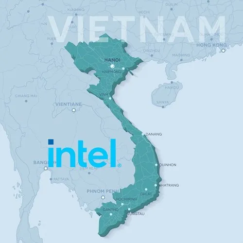
A 500,000 ft2 (~47,000 m2) state-of-the-art cleanroom facility still towers as the largest U.S. high-technology investment in Vietnam 10 years after starting operations in Saigon High Tech Park in District 9, Ho Chi Minh City. The structure built by Intel Products Vietnam (IPV) on the back of a $1 billion investment is the largest assembly and test manufacturing facility (ATM) in the Intel assembly and test network. IPV turns out products that are helping power cutting-edge applications along with the next wave of semiconductor industry growth as it homes in on 5G, Internet of Things (IoT), desktop and mobile. And it has been a boon to the local economy, generating more than 5,000 high-skill jobs across a number of assembly and test disciplines since launching operations in 2010. It has also contributed to over US$37 billion in exports from 2010 to 2019, accounting for over 60% of Saigon High-Tech Park’s annual export values in 2019. With its vision “to create the future of Intel and Vietnam,” Intel continues to be a strong long-term partner in Vietnam. I recently spoke with Kim Huat (KH) Ooi, vice president of Manufacturing and Operations and General Manager at Intel Products Vietnam (IPV), about the facility’s vital role in Intel’s overall manufacturing operations, its support for the E E ecosystem in Ho Chi Minh City, and measures it has implemented to reduce the impact of the COVID-19 pandemic on the facility and protect employees. Ooi leads and manages the site to support Intel’s business in Vietnam. His responsibilities include overseeing factory operations and employee relations; enriching the Intel image and brand; building strategic relationships with communities, media, governments, and local authorities; and working with the industry ecosystem and government. IPV employees celebrate Intel’s 50th anniversary in 2018. Ng: How does IPV campus complement the rest of Intel manufacturing sites and be nearer your customers and supplier base?Ooi: Intel Vietnam is an important part of Intel’s manufacturing presence worldwide. IPV has been operating for nearly 14 years in Vietnam and has celebrated multiple milestones along the way. As a site, we have matured and grown over the years. In March this year, we celebrated a proud milestone – the rollout our 2 billionth unit – that reflects the value of IPV to Intel Corporation as these Made in Vietnam products support its customers worldwide. One of our philosophies is to work with and grow local ecosystems in countries where we operate. In Vietnam, Intel has been offering technical and managerial expertise to many local suppliers in Vietnam to help them expand their business and services to other foreign direct investment (FDI) customers in the industry. Over the past 10 years, Intel’s supplier list has grown 10-fold from 20 in 2010 to about 180 suppliers in 2020.In today’s world of fast-changing consumer preferences and expectations, we need to help drive development of the latest products and technologies to support strong customer demand and new product portfolios such as 5G. To support evolving customer requirements, our workforce frequently upgrades its skills to work on new products and technologies.Intel as a company is also evolving as it transforms from a PC-centric to a data-centric organization, a shift behind the more than US$70 billion in record revenue Intel posted in 2019. Intel’s data-centric business accounted for more than half of that revenue. IPV plays a key role in Intel’s expansion into new market segments.Ng: What are the key differentiating elements (talent, tax, technology, trade, EHS) in Vietnam that have been instrumental in supporting the E E ecosystem in Ho Chi Minh City?Ooi: Vietnam’s stable political environment and increasingly liberalized trade and investment policies are great for businesses. The region’s young, talented workforce is also one of many competitive advantages that enables it to attract foreign investment. Intel’s announcement to invest in Vietnam in 2006 has played a large part in helping put Vietnam on the map of the global IT and semiconductor industry. The news helped attract industry suppliers and service providers, bolstering Vietnam’s economy and creating jobs. The Vietnam government also figured prominently in sparking the boon by establishing the right policies and incentives to attract foreign investment. Since starting operations, we have seen significant improvements in infrastructure such as roads, ports, airports, broadband and power supply. Vietnam’s standing in the global business community is even stronger today after the government successfully combatted the COVID-19 pandemic early on and introduced policies to help businesses restart operations. We expect all these factors to continue to make Vietnam an attractive relocation target for companies around the world. Ho Chi Minh City People’s Committee Vice Chairman Mr. Duong Anh Duc (center) visited Intel Vietnam to tour the state-of-the-art facility. Ng: What measures have you implemented to reduce the impact of the COVID-19 pandemic and protect employees? Ooi: COVID-19 has taken the world by storm and changed the way we work and live in many ways. It has unquestionably pushed the world to build stronger partnerships among individuals, organizations, businesses and communities. Intel’s manufacturing operations have continued to run at full capacity. Since the outbreak emerged, we have strictly followed required Intel safety measures as well as the Vietnam’s health guidelines. We have also implemented a number of other safety initiatives and protocols to ensure our business runs smoothly. We’re doing everything possible to ensure the well-being of our employees and help them better respond to the pandemic.In coordination with our strategic partners, we have been donating thousands of Personal Protective Equipment (PPE) to the Fatherland Front and Department of Health (DoH) since early March. Recently, in partnership with AmCham Vietnam, Intel donated an imported ambulance with built-in essential equipment to the Ho Chi Minh City 115 Emergency Center. Intel has also teamed with Saigon Hi-Tech Park management to donate two ventilators and N95 masks to DoH.Our employees are also helping out by donating to Vietnam’s Coronavirus Donation Matching campaign. We collected US$13,000 from Intel employees and included matching funds from Intel Foundation to support three non-profit organizations (NPOs) – Saigon Children’s Charity, Kidspire Vietnam and Teach for Vietnam. All told, Intel Products Vietnam has donated US$200,000 to COVID-19 relief efforts, demonstrating our long-term commitment to communities where we operate. Intel Products Vietnam teamed with AmCham Vietnam to donate a fully equipped ambulance to Ho Chi Minh City’s 115 Emergency Center, demonstrating IPV’s long-term corporate social responsibility commitment. In early May, Intel unveiled our 2030 Corporate Strategy and goals to accelerate progress against the world’s critical challenges and help drive positive global outcomes. Part of our 2030 goals, our RISE (Responsible, Inclusive, Sustainable, Enabling) strategy focuses on the company’s commitment to its corporate social responsibility (CSR) initiatives to create a more responsible, inclusive, safe and sustainable world through technology and collective action. IPV has also committed to implementing the RISE strategy in Vietnam with local community initiatives and technology interventions. Bee Bee Ng is president of SEMI Southeast Asia.
Read More
Like so much else these days, career mentoring in the semiconductor industry has gone virtual. And, among hiring managers, for good reason: Chip companies are facing a new urgency to hire skilled workers as recent SEMI forecasts spanning packaging materials and fab equipment spending show strong growth in 2021 – a trajectory that puts even more pressure on an industry confronted with a worker shortage to attract and recruit new talent.Enter SEMI Korea, which early this month gathered nearly 4,000 sheltered-in-place South Korea university students to offer tips from semiconductor industry insiders on how to kick-start their careers in the chip business. In 14 sessions over three days, industry powerhouses offered guidance across topics ranging from educational preparation and job skills to resume writing and interviewing. Like last year’s on-site event, students from Seoul accounted for the bulk of those online for Campus Outreach On-Air. But this year saw a far higher turnout of students in provincial cities thanks to the ease and convenience of virtual communications – a silver lining in the age of COVID-19.Establishing a successful career in the semiconductor industry starts with a mix of soft and hard skills, according to Changjin Kang, CEO of SEMES, one of the top 10 global semiconductor equipment companies. Keynoting the event, Kang pointed to six key attributes in particular – caring, resilience, execution, analysis, tenacity and experience – under the acronym C.R.E.A.T.E.Caring means empathy for colleagues, understanding their unique work environment and challenges, and building strong relationships. To help cope with the stress that can come with working in the industry, workers must be also be resilient by managing the emotional demands of a job and getting enough rest. Execution comes down to thorough, methodical planning. Carefully analyzing information to make data-driven decisions is a critical aspect of successful outcomes, while having the tenacity to push through difficult technical challenges helps engineers develop the right solutions. And getting out from behind the desk to learn from colleagues is important in building experience.Human resources representatives and engineers from Applied Materials, ASML, Dongjin Semichem, EO Technics, Jusung Engineering, KLA, Lam Research, Merck KGaA, Darmstadt, Germany, PSK, SEMES, SK Siltron, TEL and Wonik IPS shared with the students the key competencies needed to forge a career in the semiconductor industry. Engineers pointed to the benefits of improving their English skills through language training and continuing their education by pursuing engineering certificates. Human resources representatives stressed the importance of a global mindset since, as part of the global semiconductor ecosystem, engineers and other staff often communicate via conference calls with colleagues around the world.In a post-event survey, the students – all digital natives – awarded the event 4.3 out of 5 points for overall satisfaction and made clear that they prefer online Campus Outreach to the on-site event.“Thanks to SEMI and the companies for providing a great opportunity to meet experts and HR managers,” one student pointed out in the survey. “It was very useful because it opened up opportunities for many students to communicate with semiconductor companies.”“It was nice to know what works semiconductor engineers do,” said another, “and how as university students they prepared for employment.”SEMI Korea thanks the nine semiconductor companies that sponsored Campus Outreach On-Air to help build the industry’s talent pipeline and the students for their invaluable participation.Jaegwan Shim is a marketing specialist at SEMI Korea.
Read More
As the semiconductor industry continues to grapple with the widespread effects of the COVID pandemic, at the SEMI Foundation we continue to build programs and initiatives that inspire the next generation of STEM workers and drive new and diverse talent to all of our member companies.Our work to build out the semiconductor workforce centers on creating more diversity, equity, and inclusion within the industry. We want everyone to win. We want students and workers to benefit from these excellent jobs. We want our industry to diversify to increase our productivity, innovation, and our bottom lines. And we want to fulfill the extraordinary potential of electronics to help people around the world in the way they work and live. COVID-19 is hitting certain populations – women, veterans, and Black, Indigenous and other people of color – particularly hard, so our work has never been more timely or important for local communities and the global economy.To that end, we’re going big by generating funding and designing initiatives that will benefit the industry over the long term. The SEMI Foundation’s SEMI VetWorks Program, currently in development, will help U.S. veterans better understand our industry, the careers available to them, and how their skills will transfer to working in microelectronics. The program also provides training portals and mentorship support to smooth their transition to the industry.We’re also working to fund our Women In Industry Network, a major new initiative designed with national partners to significantly increase the representation of women, who today account for just 10-25% of the semiconductor workforce across all roles and functions. What’s more, the SEMI Foundation’s global industry image and awareness campaign is inspiring more young people to enter high-school and university STEM programs and ultimately pursue careers in microelectronics while encouraging current workers to re-skill or up-skill and join the tech workforce.Meanwhile, your High Tech U team continues to connect semiconductor companies with students all over the globe. While we’re eager to get back on the road to meet and inspire students in person, we are excited to provide updates about two of our programs:HTU in the ClassroomWith the transition to online and hybrid learning classrooms, we seized the opportunity to combine STEM activities from SEMI High Tech U with discussion sessions and other projects to help students explore and deepen their understanding of the semiconductor manufacturing process. The 16-week pilot program, called HTU in the Classroom, will launch late next year to introduce high-school students to four key areas of chip production: patterning and layering, the chemistry involved in photolithography, logic gate systems, and computational thinking. These interviews with SEMI member companies will give students a chance to share their new knowledge gained from the class and to ask questions about what life is really like as an engineer, HR professional, or manager in industry.From Sand to SiliconWith silicon the lifeblood of our industry, it is impossible to understand what makes the semiconductor/microelectronics industry tick without knowing more about the companies, processes and technologies that all make it possible. That’s why we are developing a self-guided online journey through the chip manufacturing process for students and educators. This will go beyond reading like a Wikipedia site. Instead, the learning and exploration will feature interactive elements including company videos and links to resources such as fact sheets as well as university and company websites. At each stage, students will get details about the companies and individuals who do the work and the paths the professionals followed to these roles. The big-picture look will show how all the production stages come together to build working devices that power everything from smartphones to data centers.The SEMI Foundation is grateful for your support and partnership as we all work through these unprecedented times and roll out new programs to help build the talent pipeline. To learn more about or support our workforce development programs, please contact Shari Liss, SEMI Foundation’s Executive Director, at [email protected].

Read More
On 21 September, SEMI and a coalition of 40 industry organisations sent a letter to European Commission President Ursula von der Leyen calling for decisive action to solve implementation issues within the European Union Waste Framework Directive, specifically the Substances of Concern in Products (SCIP) database.The signatories, who represent a very significant part of the European economy, are requesting urgent resolution of implementation issues for the SCIP database, which is designed to support the circular economy as defined in the European Green Deal. The database is required under Article 9.1 of the updated Waste Framework Directive.In the letter, the signatories ask President von der Leyen to take immediate action to: Postpone the SCIP notification deadline of 5 January 2021 to at least one year after finalization of the database; Conduct a study on the usefulness, feasibility, proportionality and impact of the database; Instruct the European Chemicals Agency (ECHA) to adapt the SCIP database according to the outcome of the proposed study. ECHA failed to complete development of the database by the January 2020 deadline required by the Waste Framework Directive, leaving companies insufficient time to develop, test and adapt their own systems to meet the January 2021 SCIP notification deadline.Over the last two years, the signatories have repeatedly shared their serious concerns regarding the viability, proportionality and value of the SCIP database with the European Commission and the ECHA, yet those concerns remain unresolved.Contrary to the EU Better Regulation principles that call for open and transparent decision making, Article 9.1 was added to the revised Waste Framework Directive during the final stage of the co-decision process without any prior stakeholder consultation or impact assessment. A proper impact study should help shape the way forward to deliver on the EU ambition of driving a circular European economy.Coalition PartnersEmir Demircan is director of Advocacy and Public Policy at SEMI Europe.
Read More
Solving challenges in semiconductor manufacturing requires an ongoing collaborative effort by customers, device makers, equipment and materials suppliers, and academia. ASMC 2021 will continue efforts to help the industry overcome these hurdles. To that end, we are now soliciting abstracts from industry experts across all areas of semiconductor manufacturing for presentations at the event, May 3-6, 2021 at the Saratoga Hilton/Saratoga Springs City Center in Saratoga Springs, New York.The conference provides an unparalleled platform for semiconductor professionals to network and learn the latest information in the practical application of advanced manufacturing strategies and methodologies. ASMC 2021 will be co-chaired by Ishtiaq Ahsan, Ph.D. of IBM Research and Alexa Greer of KLA.We’re looking for presentations in topic areas including the following: Advanced Metrology Advanced Equipment Processes and Materials Contamination Free Manufacturing Big Data Management and Mining Defect Inspection and Reduction Equipment Optimization Factory Automation Industrial Engineering Smart Manufacturing Yield Methodologies Click here to submit an abstract for a technical presentation. Provide an extended abstract of no more than two pages (max. of 1000 words, MS Word or PDF) with supporting data, charts, figures embedded in the last page. See author kit for details. Summarize the topic and theme in as much detail as allowed by the word count limitation. Include title, author(s), company affiliation(s), contact information, topic and five key words describing the work. The final technical manuscript must show a complete set of data to support initial abstract. Here are key deadlines and dates for industry experts to keep in mind: Abstracts Due: October 30, 2020 Author Notification: December 15, 2020 Manuscripts Due: February 9, 2021 Final Manuscripts Due: April 6, 2021 Presentations Due: April 20, 2021 Conference Dates: May 3-6, 2021 ASMC 2021 could be held as a virtual event depending on progress in containing COVID-19. Whether the event is on-site or virtual, all abstracts accepted for presentation will be published by IEEE. Speakers should be prepared to present live or online.Speakers also may be invited to publish their papers in a special section of ASMC 2021, which will be featured in IEEE Transactions on Semiconductor Manufacturing. All technical presentations will be considered for the ASMC Best Paper Award sponsored by Entegris. Students presenting an oral paper or poster will be considered for the ASMC Best Student Paper Award sponsored by GLOBALFOUNDRIES.For a complete overview of topics and other information, please visit the ASMC 2021 Call for Papers web page.Margaret Kindling is senior manager of Programs for SEMI Americas.
Read More
Every Friday I try to clear out my inbox. It’s a small way to feel like I’m on track with all the different projects we have going on at the SEMI Foundation. As I’m doing that, it’s rare that I’ll open a marketing email about a webinar, webcast, or industry event unless it’s incredibly compelling.One of them did catch my eye last week, from VLSI System Design for its VSDOpen2020.And the email did more than catch my eye. We jumped on the phone with the founders and ended up collaborating with them and the ESD Alliance on the event.The company specializes in training students in chip designs. That’s a great fit for the work we’re doing on your behalf at the SEMI Foundation and SEMI. And the VLSI System Design event is a free, online, one-day set of sessions that focus on designing digital and analog IP using freely available resources.If you have time on Saturday, October 10, I’d encourage you to check it out. They’ve got some great keynote speakers (see below), five IP designer tracks, educational sessions, and they’re even showcasing IP designed by students!It’s a great way to see some innovations in design, interact with students, and make some new contacts in a virtual setting. Below are more event details. Registration is now open.VSDOpen 2020 – Saturday, October 10Keynote speakers Jan Rabaey, the Donald O. Pederson Distinguished Professorship at the University of California at Berkeley, will offer a look at Computation in the Post-Moore Era: Reflecting on the Role of Open Source. Naveed Sherwani, Chairman, CEO and President of SiFive, will describe RISC-V and open source hardware – A golden opportunity for the India semiconductor industry. Michael Wishart, Co-Founder and CEO of efabless, will address Applying Community Models to ICs: Why and How. In addition, Jeremy Bennett, Chief Executive of Embecosm, will deliver an industry talk on A brief history of open hardware: Learning from the free and open source software movement. And Sunita Verma of the Ministry of Electronics and Information Technology will give a presentation on India’s initiatives in electronic system design and manufacturing.There are also networking opportunities for designers, researchers, tool developers, and students. If you want to go deeper, join the lab-based workshops offered in the three days (Oct 7-9) leading up to the event.Check out the full program for more on specific sessions.Shari Liss is executive director of the SEMI Foundation. She oversees SEMI Workforce Development programs from K-12 through re-skilling for veterans.
Read More