downloadGroupGroupnoun_press release_995423_000000 copyGroupnoun_Feed_96767_000000Group 19noun_pictures_1817522_000000Member company iconResource item iconStore item iconGroup 19Group 19noun_Photo_2085192_000000 Copynoun_presentation_2096081_000000Group 19Group Copy 7noun_webinar_692730_000000Path
Skip to main content
Default Banner Image

Materials

Silicon carbide (SiC) has become a cornerstone of next-generation power electronics, driving advancements in electric vehicles, renewable energy, and industrial applications. After several years of rapid capacity expansion, the SiC industry is now entering a new phase focused on optimization, quality, and long-term scalability.This transition reflects a broader realignment across the global semiconductor ecosystem. As new fabs come online and supply chains mature, the industry is prioritizing stability, cost efficiency, and technical excellence over sheer capacity growth. SiC has moved from being a niche technology to a critical enabler of the energy transition, and this maturity demands not only investment in tools and materials, but also in process knowledge, cross-industry standards, and long-term partnerships that can sustain innovation at scale.To understand how this shift is unfolding, SEMI Europe spoke with Dr. Mark Puttock, Senior Director, Technology and Innovation at Entegris. Puttock shared his perspective on the industry’s evolution and how strategic collaboration and process innovation are shaping the next chapter of SiC manufacturing.From Ramp-Up to RefinementThe early growth of SiC manufacturing was driven by surging demand for high-efficiency power devices, particularly in electric vehicles. According to Puttock, that expansion period has given way to a new focus on yield, uniformity, and process control.The industry is entering a stage of maturity where success depends on optimization rather than scale alone. Improving consistency across crystal growth, wafer, and device fabrication is becoming just as important as adding capacity. This refinement phase calls for closer integration between materials science and manufacturing technology to ensure reliability and cost efficiency.A Focus on Process and Materials InnovationAs SiC moves toward high-volume production, challenges related to contamination control, defectivity, and wafer uniformity are taking center stage. Puttock noted that addressing these issues requires collaboration between materials suppliers, equipment manufacturers, and device makers.Efforts across the industry are converging on similar goals: enhancing purity, improving process repeatability, and developing new methods to enable larger wafer formats. Moving from 6-inch to 8-inch SiC wafers, for example, is widely recognized as a key step toward higher throughput and cost efficiency. Puttock emphasized that innovation in materials science and manufacturing technology must go hand in hand to support this scaling trend.Insights from Cross-Industry CollaborationA recent Entegris blog post featuring insights from Volkswagen Group Components and Porsche Consulting explores how SiC adoption is reshaping manufacturing strategies beyond the semiconductor industry. The post also highlights the strategy paper developed by Porsche Consulting in collaboration with Entegris. This joint effort demonstrates the value of aligning semiconductor-grade precision with automotive manufacturing demands. By sharing perspectives across industries, partners can accelerate best-practice adoption and strengthen the overall ecosystem for wide-bandgap technologies.Building a Sustainable FutureSustainability remains an integral part of this optimization phase. SiC devices themselves enable energy efficiency in end applications, but the way they are manufactured is equally important. Optimizing material use, recycling process consumables, and improving chemical delivery efficiency all contribute to a smaller environmental footprint. As production scales, attention to both performance and sustainability will be key to long-term success.Looking ForwardThe transition from expansion to optimization marks a pivotal moment for SiC manufacturing. Industry focus is shifting from building capacity to mastering control, quality, and resource efficiency. Puttock sees the future of SiC as one shaped by deeper digital integration, data-driven process development, and continued collaboration across disciplines. These advancements will help enable more consistent, sustainable, and cost-effective production—laying the foundation for the next generation of high-performance power devices.At the same time, Entegris continues to invest in materials science, contamination control, and advanced process technologies that help its customers overcome the complex challenges of SiC manufacturing. By combining technical expertise with a collaborative approach, the company plays an active role in supporting the industry’s transition toward more efficient and sustainable production.James Lam is Business Development Manager at SEMI Europe.
Read More
Atomic layer deposition (ALD) and atomic layer etching (ALE) are transforming the way semiconductors are built—layer by layer, atom by atom. These atomic-scale processes are essential to scaling future transistors, improving memory, and enabling next-generation device architectures.SEMI spoke with Sergei Ivanov, Business Technology Director of Metallics R D and Balaji Kannan, Business Technology Director of Dielectrics R D and from Merck KGaA, Darmstadt, Germany to learn about their latest material innovations. At the company’s Electronics business, materials scientists and process engineers are advancing atomic-scale engineering to address some of the semiconductor industry’s toughest challenges. From novel deposition chemistries to next-generation etch techniques, their work is helping to enable future logic, memory, and specialty devices.Pushing the Boundaries of ALD Precursor ChemistryAtomic Layer Deposition (ALD) remains a cornerstone technology for scaling transistors and enabling new architectures. Materials scientists at Merck KGaA, Darmstadt, Germany are exploring novel precursors that enhance film quality, streamline processes, and expand the operational window for complex structures:One area of focus is next-generation hafnium and zirconium precursors. “These advanced high-k dielectrics offer better thermal stability, improved step coverage, and reduced impurities while achieving higher k-values,” Sergei Ivanov explained. “Such attributes are essential for logic and memory devices that demand reliable dielectric performance with minimal defect density.”Another important development is area selective deposition (ASD). Merck KGaA, Darmstadt, Germany’s small-molecule inhibitor solutions reduce the need for advanced patterning in narrow dimensions and 3D geometries, enabling cost-effective and simpler integration for leading-edge nodes. Their selective co-reactants platform leverages digitalization techniques including multivariate analysis, digital twin technology, and machine learning to accelerate process development for critical ASD applications. This approach facilitated industry-first adoption of ASD in high volume manufacturing and enables an ever-expanding toolbox of OEM processes for ASD of high-k, Ti, Mo, Si and other thin films.Merck KGaA, Darmstadt, Germany is also broadening the scope of ALD chemistries across the periodic table. “As our customers encounter new technical challenges, we continue to expand our R D scope across new elements and ligands. Examples include europium, lanthanum, scandium, and cerium dopants with improved electrical properties, niobium and vanadium precursors for deposition of nitride and oxide films with reduced impurities and improved ALD performance, and high-performance nickel MILC solutions are finding their way out of our labs and into customer roadmaps at an ever-accelerating pace,” said Sergei Ivanov.The company’s role in molybdenum chemistry is another example. Merck KGaA, Darmstadt, Germany is a key producer of molybdenum precursors including MoO2Cl2 with industry-leading quality, density, and container utilization. The company offers MoCl5 with advanced trace impurity control paired with innovative container technology. The company’s next-generation organic metallic molybdenum precursors incorporate novel ligands that contribute to critical gains in device performance.Merck KGaA, Darmstadt, Germany’s work with organosilane precursors is also opening new possibilities. “For gate-all-around (GAA) transistor technology, precursors incorporating novel bonding structures enable highly conformal dielectric films with excellent electrical and physical properties, even in complex 3D geometries. At the same time, organosilane chemistries designed to increase silicon incorporation during deposition are supporting high-growth-rate oxides for gapfill applications, delivering the thick films required with greater throughput,” said Balaji Kannan. “Together, these innovations highlight how tailored precursor design can address both scaling challenges and manufacturability in next-generation devices.” Driving Selective and Sustainable Atomic Layer Etching (ALE)“Precision in etching is as critical as deposition. Our innovations in ALE are designed to provide ultra-selective, low-damage material removal, which is increasingly vital as device geometries become finer and more complex,” Sergei Ivanov shared. One example is metal-free ligand exchange ALE for high-k materials, where Merck KGaA, Darmstadt, Germany’s research into etching HfO₂, ZrO₂, and HfZrO₄ showcases a novel metal-free approach. This technique enables accurate and damage-minimized etching of high-k dielectrics, which is essential for integrating advanced transistors and memory stacks.These advancements address industry-wide concerns regarding pattern fidelity, material selectivity, and plasma-induced damage, ensuring greater process control and extending the lifetimes of devices.Looking AheadMerck KGaA, Darmstadt, Germany’s strategic commitment to semiconductor innovation includes ongoing R D efforts that reflect the vision of its Electronics business: providing material-centric solutions to the industry’s most complex integration and performance challenges. Whether advancing front-end device scaling or developing breakthrough materials for emerging applications, the Electronics business of Merck KGaA, Darmstadt, Germany is committed to shaping the materials roadmap for a more connected, intelligent, and efficient world.James Lam is Business Development Manager at SEMI Europe.
Read More
AI is proliferating rapidly, fueled by ever-larger models and data sets that are expanding AI use cases and improving its accuracy. Future computing systems are now required to simultaneously deliver high performance, process large amounts of data, and use the least possible energy. The growing energy footprint of AI and the strain it places on the power grid is an increasing concern for companies and even entire countries. This could adversely impact future growth and could slow the semiconductor industry’s march towards $1 trillion in revenue, which is largely driven by AI applications.This is a formidable challenge that cannot be addressed in silos by individual companies or even industry segments. The SEMI Smart Data-AI Initiative is exploring how to overcome this challenge with collaborative and innovative system-level solutions that connect the dots across the entire AI system stack. In March 2025, we hosted a successful workshop, bringing together industry leaders across the value chain for a day of thoughtful discussions and knowledge sharing. Building on this foundation, we developed an exciting Smart Data-AI session to be held at SEMICON West in Phoenix, Arizona on October 7 from 10:30 a.m.-4:40 p.m. The “Future of Computing: Energy-Efficient Computing for AI and Beyond” forum will bring together executives and thought leaders across the entire ecosystem – including design, fabrication, interconnects, system integration, hyperscale architectures, advanced materials, and emerging technologies such as photonics and quantum. Attendees will have a unique opportunity to get strategic perspectives from these distinguished experts and learn about exciting future trends.Why Attend?Gain insights from global leaders and learn about innovative paths towards an energy-efficient computing future.Network and build cross-industry collaborations for the next wave of AI, photonics and quantum.Promote a more sustainable path for continued growth of AI to benefit humanity and the planet.Join the SEMI Smart Data-AI initiative to develop solutions and take concrete actions to reduce AI’s growing energy footprint.Support the industry in achieving its goal of reaching $1 trillion in revenue. Speaker Highlights Include:AMD • Ciena • Hewlett Packard Enterprise • IBM • Merck KGaA, Darmstadt, Germany •Microsoft • Quantum Economic Development Consortium • Rapidus • Rigetti •Siemens AG • Stanford UniversityDr. Pushkar P. Apte is the Strategic Technology Advisor and leads the Smart Data-AI Initiative at SEMI.
Read More
As artificial intelligence (AI) proliferates rapidly, AI models and datasets are also growing rapidly in size. This growth far outpaces performance improvement in hardware systems, and is increasing AI’s energy consumption unsustainably. To address these challenges and explore collaborative solutions, SEMI’s Smart Data-AI Initiative - as part of its Future of Computing focus - recently hosted a day-long workshop on Sustainable AI Systems that brought together domain experts from the entire AI ecosystem. Speakers included industry leaders Applied Materials, AMD, Arm, ASE, Google DeepMind, IBM, Intel, Lam Research, McKinsey, Micron, NVIDIA, Qualcomm, SK hynix; exciting start-ups Cerebras, LightMatter, Mentium Technologies and Mueon; and leading-edge academic institutions, Stanford University and University of California, Davis Irvine. The keynotes, panels and spirited audience discussions covered novel devices, materials, advanced packaging, chiplets, photonics and architectures algorithms for data centers, cloud edge. This article synthesizes high-level insights from the workshop.The AI ImperativeThe day started with a basic question – why is AI essential to continued progress and prosperity? The answer lies partly in shifting global demographics, with the population aging in most developed economies. At the turn of the century, there were ~6 people in the workforce supporting each retiree, but projections indicate there will be only 2 active workers per retiree by 2050. In parallel, productivity growth rates have fallen to half of what is required. AI can help bridge this gap, if we can ensure continued progress of AI in a responsible and sustainable manner.The Energy WallA formidable roadblock to continued progress of AI is its rising energy demands. For example, the energy used by some large language models (LLMs) to run just one training cycle could be used to power thousands of homes. The switch to transformer models has increased AI-driven computing demand by a factor of 50 million over 5 years, and by some projections, this demand will consume half the world's generation capacity by 2050. This is clearly not sustainable! All players in the ecosystem are deeply committed to reducing AI’s energy consumption, and the industry has already decreased the energy used per token of computing by a factor of 100K in the past 10 years. However, the rapid growth of AI outpaces this, highlighting the huge challenge ahead.The System StackThis workshop was developed with the hypothesis that innovation is required across all segments, and an important first step is to initiate a dialog. Our highly distinguished speakers covered the entire solution stack, and while it is impossible to capture the ocean of insights that they shared, the following provides a flavor.Materials DevicesMaterials and devices used to build semiconductor chips form the foundation of the stack for all computing systems. Silicon substrates with copper interconnects remain industry’s mainstay, but are being augmented by innovative ideas. As device dimensions continue to shrink, novel 2D materials such as MoSe2, WSe2, ZrSe2 and NbP are being researched. While Si mobility degrades with decreasing film thickness, 2D materials maintain high electron mobility in thin-film substrates. These can be stacked to build 3D systems with lower power consumption than traditional planar structures. In parallel, novel device technologies such as gate-all-around (GAA) can provide power savings up to 25%.These novel materials and devices are complex, and require almost magical wizardry to build. For example, they may require depositing a stack of multiple defect-free films that are only a single (or few) atomic layer(s) thick, or etching a steep well that is one hundred times as deep as it is wide. It is an incredible accomplishment of the semiconductor industry to build these devices and chips successfully, but it is getting harder and more expensive. Consequently, AI is now being used as a tool to help with this ever-growing fabrication complexity of semiconductor R D and manufacturing. This is a synergistic virtuous cycle, where AI algorithms enabled by chips are used in turn to help with chip fabrication.System IntegrationThe next layer of the stack is the integration of individual devices into a system. Advanced packaging techniques, such as silicon or glass interposers (2.5D) for interconnecting chips, can reduce the communication distance and power consumption. These are often deployed for high-performance computing systems running AI algorithms. Beyond this, the industry is actively exploring 3D systems that are even more compact, both as multi-die 3D packages and as monolithic 3D chips.The concept of chiplets – smaller chips with specialized functions that can be assembled flexibly to optimize system performance – holds much promise. Industry consortia are developing protocols such as Universal Chiplet Interconnect ExpressTM (UCIeTM) to enable seamless integration of chiplets both in the planar and vertical dimensions. These advanced techniques pack more functional elements into increasingly compact form factors, but this proximity makes power delivery challenging and often generates intense heat. Much work is needed to ensure optimal power delivery and adequate thermal dissipation.Looking beyond traditional electronics, photonics represents an exciting opportunity. Most long-distance data communication is on fiber-optic cables and thus already photonic – bringing this to shorter distances can save energy while increasing bandwidth and performance. This requires efficient photonic-electronic integration at the packaging or even chip level, which is a major challenge requiring cross-disciplinary collaboration.Architectures and AlgorithmsAI algorithms need enormous amounts of data processing compared to traditional computing workloads. This requirement stretches (or breaks) the limits of traditional Von Neumann architecture, which requires frequent data movement between memory and processor elements for each computation cycle. Much of current architecture innovation focuses on bringing processor and memory elements closer to each other. System integration is already driving “compute-near-memory” architectures like high bandwidth memory (HBM). Other forward-looking implementations combine them into a single chip, known as compute-in-memory (CIM). Memory elements being explored for this purpose include resistive RAM (RRAM), phase-change memory (PCM), ferroelectric RAM (FeRAM) and magnetic RAM (MRAM). However, there is no one “perfect” memory – each has pros and cons in terms of latency, capacity, bandwidth, power consumed per operation, manufacturability, etc. Other researchers are also exploring devices like memristors for analog computing, which can improve energy efficiency for certain workloads.Finally, hardware-software co-optimization is crucial. Algorithms mismatched with the underlying system are energy expensive; conversely, co-optimized systems are highly efficient. While conceptually obvious, this is difficult in practice because development cycles are quite different – software algorithms can transform in a few months, while new hardware often takes years to develop. While some strategies can be used for mitigation – such as designing in redundancy/flexibility or making the hardware application-specific – much work remains to solve this conundrum.Pre-competitive Collaboration to Find SolutionsAll speakers emphasized that pre-competitive collaboration across the entire stack is critical, as these challenges are formidable and cannot be solved by one entity or in isolated silos. SEMI is a global and neutral organization with over 3,000 member companies, and is well-positioned to provide a pre-competitive collaboration platform to connect the dots across silos. In fact, SEMI’s mantra is “Connect, Collaborate, Innovate” – reinforcing its commitment to advancing the entire industry. For this purpose, SEMI’s Smart Data-AI Initiative continues to drive robust discussions on this topic – next there will be a roundtable discussion during SEMICON Southeast Asia, May 20-22 in Singapore, followed by a focused technology session at SEMICON West 2025, October 7-9 in Phoenix, Arizona. The overall objective is to move from “talking-the-talk” to “walking-the-walk,” towards creating system-level solutions for energy-efficient AI computing. Specifically, we want to identify the pre-competitive actions that could synergize individual innovations and make the whole greater than the sum of parts. Some ideas include collaborative proof-of-concept projects, industry standards and independent benchmarking. Come join us on this journey and connect with us at [email protected]. Dr. Pushkar P. Apte is the Strategic Technology Advisor and leads the Smart Data-AI Initiative at SEMI.
Read More
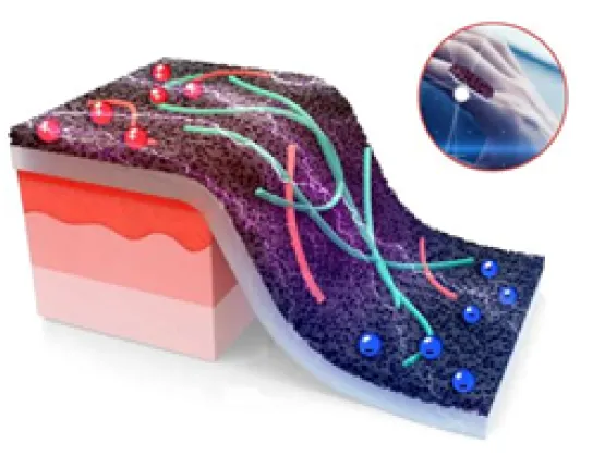
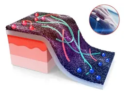
Say ‘Ahhhh’ – imagine your doctor monitoring a health condition from afar or emergency responders receiving real-time alerts that could save a life. A new smart sensor is taking the ouch out of wound monitoring. By using laser-induced graphene (LIG), a two-dimensional (2D) material, researchers are developing a sensor that could revolutionize the tracking of wound healing and recovery. Doctors could get a much clearer picture of the healing process, identifying issues like inflammation, physical strain or a spike in body temperature early on. "This unique sensor material we've developed has potentially important applications in health care monitoring,” said Huanyu “Larry” Cheng, James L. Henderson, Jr. Memorial Associate Professor of Engineering Science and Mechanics (ESM) at Penn State. LIG sensors are self-powered which means they could be especially useful for continuous monitoring in clinical settings or helping detect fires in remote locations. Source: Materials Research Institute, Penn StateUnder the Sea – Mechanical engineers at Carnegie Mellon’s Soft Machines Lab have created a soft robot inspired by the quick and agile brittle starfish, the first mobile and untethered underwater crawling robot. Named after Sponge Bob Square Pants’ sidekick, PATRICK is an AI powered robot which operates without motors so as not to disturb delicate sea life. To make the robot move, the researchers hit it with electric current, causing the wires to heat up past its transition temperature and allowing the limbs to contract and move in different directions. “We want to put the power and the electronics on-board with the robots,” said Ph.D. candidate and PATRICK creator, Zach Patterson. The soft robotic systems which are ideal for tracking the health and quality of water, are biodegradable to eliminate waste and protect the natural environment.Source: Carnegie Mellon University, School of Engineering The sky is NOT the limit with engineering – While Blue Origin made the news recently for sending an all women crew to the edge of space, the first Mexican born woman to travel into space is Katya Echazarreta, an electrical engineer originally from Guadalajara, Mexico. Echazarreta was selected for the trip from a pool of 7,000 applicants from more than 100 countries based on her outstanding achievements in the space industry, including five NASA missions. She traveled to space in 2022 aboard Blue Origin’s NS-21 flight as one of Space for Humanity’s citizen astronauts. Echazarreta comes from a family of engineers and works to make space exploration accessible to young kids, teens, women, and other scientists and engineers through Fundación Espacial, a foundation started in Mexico. Source: Astronomy.comMargaret Kindling is Senior Program Manager at the SEMI Foundation. She promotes inclusive workplaces via initiatives including Women in Semiconductors, Semiconductor PRIDE and workforce and career development programming at SEMICON West and SEMIEXPO Heartland.
Read More
In a world where technological advancements move at lightning speed, the semiconductor industry is facing unprecedented challenges. The demand for smaller, faster, and more energy-efficient devices is growing, and traditional manufacturing processes are being pushed to their limits. Enter Spin-on Dielectrics (SOD), a breakthrough material technology that offers a cost-effective, scalable solution for micro-gap filling and high-performance dielectric films. As the industry evolves, SOD is expected to play a pivotal role in enabling the next generation of chips that power everything from AI to everyday electronics.To learn more, SEMI Europe and Merck KGaA, Darmstadt, Germany, held a joint webinar that focused on semiconductor device process evolution by SOD. The session featured insights from three technology experts in the company, including Dr. Surésh Rajaraman, Executive Vice President and Head of Thin Film Business Unit, along with Atsuko Yamamoto, R D Manager for Spin-On Dielectric, and Go Nakano, Global Marketing Manager for Dielectric Materials.SEMI: What is SOD, and how does it fit within the broader semiconductor manufacturing process?Rajaraman: SOD, Spin on Dielectrics, is a unique class of materials used to deposit thin layers of dielectric films, which act as insulators or other functional films, on semiconductor devices. The fabrication of a semiconductor chip involves thousands of intricate steps that incorporate conductors, semiconductors, and insulators. SOD is a versatile technology that supports device performance and miniaturization by enabling better gap fill and film uniformity, all while offering attractive cost of ownership.SEMI: Why is there so much focus on SOD materials, and how are they evolving to meet future industry demands?Rajaraman: As semiconductor devices become more complex—such as 3D NAND scaling to more than 300 layers and DRAM incorporating pillar capacitors—there’s a growing need for materials that can address challenges like interconnect delays, power consumption, and heat generation while maintaining optimal performance. Traditional dielectric materials are reaching their limits, making Spin-on Dielectrics (SOD) a critical solution. SOD offers advantages like bottom-up and seam-free gap filling, enabling ultra-thin insulating and other functional layers that enhance electrical and thermal efficiency and support next-generation device scaling.The industry is pushing the boundaries of scaling, with increasing aspect ratios and complex structures in Logic, 3D NAND and DRAM. Modern devices now require deposition in features which are not only incredibly narrow but also increasingly deep due to going into the third dimension. This creates new challenges, such as stress buildup and cracking in conventional SOD materials. To overcome this, we are developing enhanced formulations with improved mechanical stability and polymer backbone engineering. These innovations enhance gap-filling properties and resistance to process-induced stress, ensuring SOD remains a key enabler for advanced semiconductor manufacturing.SEMI: What are the current industry trends driving the adoption of SOD?Nakano: SOD is becoming a key technology because of its excellent gap-filling performance. Unlike gas-phase deposition methods like Chemical Vapor Deposition (CVD) and Atomic Layer Deposition (ALD), SOD is a liquid-phase process. This makes it more efficient for high-aspect-ratio structures. It also helps reduce costs while maintaining high-performance dielectric properties.With increasing demand for high-density memory and logic devices, SOD is crucial for applications like DRAM and NAND flash, which require precise dielectric layer formation. In DRAM, we’re witnessing a shift from planar to vertical transistors, and even to monolithic 3D DRAM. These changes require new materials for gate insulators and electrodes, alongside improvements in aspect ratio gap filling.For NAND memory, manufacturers are increasing the number of memory layers, leading to taller memory stacks and deeper trenches. As lateral scaling progresses, narrower and more complex structures demand high-aspect-ratio trench fills to maintain performance and reliability.Logic devices are also evolving, with transistor structures moving from FinFETs to nanosheets and forksheets. This transition enhances performance, but it also introduces challenges in wiring density and electrical properties. The narrower pitch of wiring requires advanced dielectric solutions, like SOD, to enable reliable, high-performance semiconductor architectures.SEMI: With all these recent innovations, what role does Merck KGaA, Darmstadt, Germany play in supporting these advancements, and what does the company offer its customers? Rajaraman: As the semiconductor industry pushes the boundaries of scaling, doing so requires materials that can support increasingly complex structures. We are the only materials company in the industry to possess the full spectrum of process technologies for gap-filling capabilities, including SOD, ALD, CVD, and Flowable CVD. Our strategic acquisition of Versum Materials has expanded our capabilities with organosilicon precursors. Combined with our SOD expertise, it allows us to reengineer material backbones with more material choices and tailored properties to optimize performance in high-aspect-ratio applications.To support this, we’ve expanded our global R D footprint. We now operate in various application labs, enabling close collaboration with customers for material customization and fine-tuning properties to address specific manufacturing challenges. Last year, we inaugurated a new R D center in Korea as part of our commitment to being near our customers and accelerating time-to-market for next-generation semiconductor solutions. As semiconductor roadmaps become more complex, customization and collaboration also become more critical. The key to innovation lies in working closely with our customers, understanding their challenges, refining materials, and optimizing processes together. By fostering this ongoing partnership, we can accelerate technological advancements and ensure that new solutions align seamlessly with evolving industry demands.SEMI: Can you share some technical insights on SOD?Yamamoto: SOD is a key material used in semiconductor manufacturing to create insulating layers with high precision. One of the essential components in SOD is PHPS (Perhydropolysilazane), a polymer composed of silicon, nitrogen, and hydrogen. This material is applied as a liquid solution and transforms into a high-quality silicon oxide film through a series of thermal processes.PHPS is essential because it enables precise gap filling in extremely small structures, helping to improve device reliability. The process involves spin-coating the polymer onto a wafer, followed by pre-baking to remove solvents. Then, it undergoes high temperature curing in an oxygen and steam atmosphere, forming a dense silicon oxide film. This method ensures uniform coverage and cost efficiency compared to traditional dry film deposition techniques.Our Spinfil® product line has evolved over the past two decades, starting with the Spinfil® 400 series and advancing through the Spinfil® 600 to the widely used Spinfil® 800 series. These improvements have enhanced gap-filling capabilities and film uniformity, making them ideal for high-aspect-ratio trench structures. The critical baking process involves spin coating and pre-baking before wafers undergo batch processing in a high-temperature furnace. Controlled temperature and moisture conditions transform Spinfil® into silicon oxide films, optimizing properties such as refractive index, shrinkage, and etching resistance and ensuring reliability in semiconductor applications.SEMI: What are the latest trends in new polymer development for SOD?Yamamoto: Our research focuses on three key areas: enhancing film quality, developing SOD for high-aspect-ratio trench filling, and advancing low-k SOD for semiconductor processes.To improve film quality, we introduced the Neofil®series, an evolution of the Spinfil® 800 series. This innovation reduces film shrinkage, lowers stress, and enhances wet etching rates, making it ideal for next-generation semiconductor nodes.Our latest Neofil® series for high-aspect-ratio trench filling is targeted for traditional dry processes like CVD and ALD, which can often lead to void formation and require multiple deposition-etch steps. Our latest SOD materials address this by improving polymer elasticity, ensuring uniform filling of deep trenches up to 16 microns without cracks, making them suitable for emerging 3D nanostaircase designs.In low-k SOD development, we’re focusing on siloxane-based polymers, which provide excellent trench-filling capabilities while maintaining strong mechanical and electrical properties. Compared to flowable CVD and ALD, SOD offers a more cost-effective and efficient alternative. With continued advancements, we anticipate SOD will become a key material for future semi-damascene processes, enhancing embedding performance and overall device reliability.SEMI ContactSitong He, Communications Manager Email: [email protected]
Read More
Superconducting Naturally – Miassite is a naturally occurring mineral which scientists at Ames National Laboratory have identified as the first unconventional superconductor found in nature. Unlike conventional superconductors that follow the Bardeen-Cooper-Schrieffer (BCS) theory, minerals such as miassite exhibit unique properties outside of this framework. Made of rhodium and sulfur, miassite was initially recognized as a regular superconductor in 2010. Recent tests confirm it joins a small, exclusive group of unconventional superconductors previously limited to lab-made materials.Lab tests on miassite involved measuring magnetic reactions, inducing defects, and analyzing energy gaps, all confirming its unconventional behavior. While naturally occurring, samples are unlikely to be superconductive due to their disordered state, miassite’s lab-verified properties open doors to new research and highlight its unique duality as both a conventional and unconventional superconductor.Source: A Superconductor Found in Nature Has Rocked the Scientific WorldPheromones + vision = mate selection – When choosing a mate, Heliconius butterflies, despite their tiny brains can outperform current AI in multi-sensory decision-making by processing visual and chemical cues simultaneously. This discovery inspired Penn State researchers to develop a low-energy, multi-sensory AI platform using 2D materials. The device combines molybdenum sulfide (MoS2) to mimic visual capabilities and graphene to detect chemical signals like pheromones.The device could integrate visual and chemical cues, offering adaptability like a butterfly’s mating behavior. This innovation addresses limitations in current AI, which relies heavily on energy-intensive, single-sensory processes. Researchers aim to expand the device to process three senses, like crayfish using visual, tactile, and chemical cues. The work, supported by the U.S. Army Research Office and the U.S. National Science Foundation, could revolutionize applications in robotics, smart sensors, and critical environments, by enabling AI systems to detect issues using multiple sensory inputs efficiently. Imaging of Heliconius Butterfly A Butterfly Effect – Proving once again that there is a lot to be learned from nature, researchers from the Fraunhofer Institute for Solar Energy Systems ISE have developed innovative, colored solar facade elements inspired by morpho butterfly mimicry. These panels are aesthetically pleasing, integrate seamlessly into building exteriors, and retain high efficiency, achieving 95% of the power output of uncoated panels. Using vacuum-applied 3D photonic structures like those on butterfly wings, the panels produce vibrant, angularly stable colors with minimal energy loss. This MorphoColor® technology addresses architects’ and building owners’ concerns about design, offering an efficient, visually appealing solution for building-integrated photovoltaics while surpassing other technologies currently available.Close up of a morpho butterfly wingSustainable Flight – The world’s fastest supercomputer, Frontier, located at Oak Ridge National Laboratory, enables unprecedented advancements in sustainable aviation technology. Capable of over a quintillion calculations per second, Frontier allows GE Aerospace to conduct full-scale simulations of its revolutionary Open Fan engine design, accelerating insights into aerodynamics and turbulence. This groundbreaking tool aids the CFM RISE program, which aims to cut fuel consumption and CO2 emissions by at least 20%. Frontier’s detailed simulations predict engine performance under real-world conditions, saving years of testing. The partnership between GE Aerospace and Oak Ridge is expanding, promising future collaborations in climate modeling and advanced simulation techniques.An Open Fan engine design developed as part of a new project led by GE AerospaceSource: https://www.geaerospace.com/news/articles/new-frontier-how-ge-aerospace-using-worlds-fastest-supercomputer-help-design-open-fanMargaret Kindling is Senior Program Manager at the SEMI Foundation. She promotes inclusive workplaces via initiatives like Women in Semiconductors, Semiconductor PRIDE and workforce development programming at SEMICON West and SEMIEXPO Heartland.
Read More
Integrated photonics offers the semiconductor industry a new way to increase the speed and capability of classical compute functions, as well as enabling quantum computing. The III-V Summit, hosted by SEMI Europe in partnership with Photon Delta at SEMICON Europa, opened with a compelling question: why is a photonics summit taking place in the middle of a semiconductor event? Ajit Manocha, President and CEO of SEMI, highlighted the growing convergence of the semiconductor and photonics industries, stating, “It is my firm belief that a boost to Moore’s Law will come from the III-V world.” Declaring that the rate of growth in integrated photonics is set to pick up substantially, Manocha assured, “I will be your ambassador to make sure that the III-V technologies gain far greater visibility than they have today.”Ajit Manocha, President and CEO, SEMIThe promise of new III-V technologies is generating significant excitement within the semiconductor industry. Abdul Rahim, Ecosystem Manager at PhotonWorld, acknowledged the reality that today’s III-V device industry operates in a limited sphere, stating, “The III-V world is still at the interface of industry and academia. There is one main application for III-V devices – transceivers for data centers.” Abdul Rahim, Ecosystem Manager, PhotonWorld Carlos Lee, Director General of the European Photonics Industry Consortium (EPIC), echoed this message, “Photonics is not so much an industry today; it’s an ecosystem. It lacks the standards, roadmaps, and market data that a full-fledged industry needs – but we are getting there.” Carlos Lee, Director General, European Photonics Industry Consortium (EPIC)However, Rahim pointed to a number of trends that are driving the growth of III-V technology for integrated photonics. One key development is large-scale integration, “over the years, the number of devices in one photonics integrated chip (PIC) has been growing fast, reaching tens of thousands of components on-chip,” Rahim explained. Additionally, the widening frequency range supported by III-V devices is unlocking new applications beyond the telecom sector. Broad Scope of Research into III-V Technology for Integrated PhotonicsResearch into III-V technology spans an impressive range of materials, processes and applications. Nick Singh, CTO at Compound Semiconductor Applications (CSA) Catapult, a government-backed technology incubator, described in detail the most important fields of research that are driving innovation in integrated photonics. “III-V materials are special because they can be engineered,” Singh explained. Highlighting their potential role in advancing quantum computing, Singh added, “The ability to use new materials is crucial to reducing the reliance on algorithmic compensation for errors and non-linearity in hardware.” Nick Singh, CTO, Compound Semiconductor Applications Catapult However, Singh emphasized the need for the photonics industry to address structural challenges that could hinder progress. “Collaboration is crucial to standardize process development kits (PDKs) for photonics device fabrication processes—it’s like the Wild West in PDKs right now,” Singh remarked. “Additionally, the availability of raw materials presents a significant challenge.”The truth of this warning was confirmed by Diane Scott, Vice President of TECHCET, stating, "The US has deemed gallium to be the number one supply chain risk among a list of 50 raw materials, and the European Union (EU) has identified gallium as a critical raw material."Diane Scott, Vice President, TECHCETSuch geopolitical concerns have done little to dampen the intensity of research in III-V technology. One of the powerhouses of integrated photonics research is IBM, and Heike Riel, a Fellow at IBM Research with a special interest in quantum computing, revealed promising avenues that IBM is exploring. “IBM has developed local III-V-on-silicon heteroepitaxy, “Riel explained. “Using a direct growth method, we can grow vertical, lateral, and even 3D structures in III-V, such as stacked GaAs structures.” Riel highlighted the potential applications of this technology in emerging processor designs, including the Artificial Intelligence Unit (AIU) and analog computing devices with in-memory logic. “Here, we can deploy GaAs as a photorefractive material, used as a grating, to perform the same function as conventional electronic non-volatile memory in an analog computer chip,” Riel noted. Heike Riel, IBM Fellow, IBM ResearchAlso at the forefront of photonics integration is Black Semiconductor, a start-up company based in Aachen, Germany, which is developing devices using graphene. Cedric Huyghebaert, CTO of Black Semiconductor, shared the company’s vision, “We want to use electronics to compute, and photonics to transfer data, and bring both functions together on the same chip.” Black Semiconductor’s mission is to become the first foundry to offer integrated graphene technology. “Our ambition is to integrate graphene in line with semiconductor standards using semiconductor tools – avoiding the need for exotic processing technologies,” Huyghebaert explained. “We also aim to demonstrate co-integrated photonics on a 300mm wafer system, regardless of the process node. In doing so, we want to prove that deep technological innovation of this kind is possible in Europe.”Cedric Huyghebaert, CTO, Black Semiconductor GmbH Bringing Integrated Photonics to the MassesAs III-V technology develops to enable a broader range of integrated photonics applications beyond the telecom market, experts are recognizing the need for it to become more accessible if it is to be adopted by a wider range of manufacturers. Joni Mellin, manager of the photonics business line at the X-Fab Group, emphasized, “As an industry, we need to bring electronics design automation (EDA) tools up to a level of capability that matches that of the silicon world, so that you do not need a PhD to do product design – we need to make it accessible to ordinary electronics engineers.” Joni Mellin, BL Manager Photonics, X-FAB GroupAdoption of the technology also requires access to production capacity. Peter Maat, Senior Product Manager at SMART Photonics, an open foundry for indium phosphide (InP) programmable interface controllers (PICs), highlighted the challenges in this area. Maat explained that the availability of the foundry as “not a trivial capability,” because many InP fabs are run by integrated device manufacturers, and are closed to other users. The SMART Photonics business model aims to provide a comprehensive enablement service for fabless manufacturing of PICs. “Our responsibility is to produce stable, manufacturable building blocks that we make available to designers and to provide a platform which enables our circuit building blocks to be combined into an integrated photonics circuit,” Maat said.Peter Maat, Senior Product Manager, SMART Photonics Jayakrishnan Chandrappan, Head of Advanced Packaging Technology at CSA Catapult, also emphasized the importance of access to production capability. “The CSA Catapult has one of the world’s only sub-10micron hybridization facilities for advanced packaging that is open to third-party users,” Chandrappan noted.Jayakrishnan Chandrappan, Head of Technology, Head of Technology - Advanced Packaging, Compound Semiconductor Applications CatapultPromising Future for Integrated PhotonicsAs the summit concluded, the atmosphere was charged with optimism about the future of integrated photonics. The discussions highlighted how III-V materials, combined with advanced packaging, are set to play a pivotal role in shaping next generation technologies. A recurring theme throughout the event was the profound impact III-V materials will have, as they poised to become a corner stone of virtually every emerging technological advancement. SEMI ContactLaith Altimime, President of SEMI EuropeEmail: [email protected]
Read More
Demand for hi-tech manufactured goods is at an all-time high and is expected to grow significantly in our new digital age, COVID-19 economy. This is especially true for semiconductor chips. Chip manufacturers have been working to meet this demand by building new factories and by optimizing processes and equipment in existing fabs. While there is much media coverage about new factories planned by leading-edge chipmakers and government investments in the semiconductor sector, greenfield fabs entail significant capital expenditures and are sometimes fraught with complex political concerns. As a result, they can take several years to complete and reach their planned production capacity. Instead, the semiconductor industry needs to optimize existing factories in order to increase productivity and yield and meet growing demand by implementing smart manufacturing solutions. Smart manufacturing solutions will inherently reduce costs with more efficient and automated processes, and those savings can be reinvested for the next wave of solutions. Chip Industry on the Bleeding Edge Semiconductor manufacturers have always been focused on bleeding-edge technology to outflank strong competition and build the best products – faster and cheaper. Today, pioneering organizations are using data to optimize manufacturing processes and equipment, a practice known as Smart Manufacturing. While there are many definitions of Smart Manufacturing, the essence is maximizing the utility of big data generated in these factories by leveraging three pillars: Sensing, Connecting, and Predicting. It is not just the digitization in manufacturing, but it is also about turning the data into actions that generate value – an effort the SEMI Smart Manufacturing Committee is driving based on the three pillars. Optimizing return on investment is the ultimate goal. SEMI Smart Manufacturing Initiative activity is based on three pillars that support the goal of increasing ROI. Making the Right Decision, Faster Smart manufacturing practices enable organizations to make the right decisions and take action faster based on insights generated from real-time and historical data. This requires data management technologies and applications that can process, analyze, and act on information instantly. It has become ever more difficult to process and discern the relevant data or signal from the vast volume of data, perform analytics or develop new ML or AI analytic tools, and then make the critical decisions to solve problems as close to real-time as possible. Who’s Responsible – IT or OT? In the past IT (Information Technology) and OT (Operations Technology) were separate entities within organizations, with IT focused on storing large amounts of data for enterprise systems and OT concentrated on using data to perform specific functions. Smart Manufacturing often demands combining IT and OT, difficult in rigid organizations that operate the two organizations independently and lack the infrastructure to implement comprehensive solutions. Success requires executive leadership sponsorship, motivated technical personnel and, most importantly, a clear deliverable on the value in implementing Smart Manufacturing. Many organizations have introduced top-level leadership positions such as a Chief Information Officer or Chief Data and Analytics Officer to address this convergence and many of these leaders are embracing Smart Manufacturing practices. The SEMI Smart Manufacturing community includes many of these leaders and therefore has highlighted the importance in the return on investment for Smart Manufacturing solutions. Read more about IT and OT convergence and note that Smart Manufacturing is synonymous with Industry 4.0. The SEMI Smart Manufacturing Initiative covers the entire supply chain. Get Smart in Smart Manufacturing While new technologies and applications are being created to deal with mountains of data, it is the underlying methodologies and practices that are key to a successful Smart Manufacturing deployment. SEMI, the trade association representing the electronics manufacturing and design supply chain, is in a perfect position to evangelize Smart Manufacturing experiences and best practices for the entire manufacturing community. The more than 30 member companies participating in the SEMI Smart Manufacturing Initiative bring more than 500 years of collective experience and knowledge to the topic. Many segments of the supply chain participate in the SEMI Smart Manufacturing Initiative including packaging, assembly, SMT and PCB assembly, test, software, data management, sensor and material suppliers. Learn How to Manufacture Smarter SEMI SMART Manufacturing is hosting two great conferences in the coming months – the Global Smart Manufacturing Conference (GSMC) and the SEMICON West Smart Manufacturing Pavilion. As a leader of the organizing committee and chair for the SEMICON West Smart Manufacturing Pavilion, I encourage people who want to learn how to implement Smart Manufacturing or expand their knowledge of Smart Manufacturing to attend these events. The GSMC will feature keynotes highlighting the value of Smart Manufacturing, offer tutorials on the three pillars, and introduce several case studies for each of the pillars. Thirty-two organizations – ranging from global cloud providers, semiconductor factory operators, leading equipment vendors and software application solution companies – will present. See the full agenda here. The SEMICON West Smart Manufacturing Pavilion will compliment GSMC by showcasing a number of use cases that highlight the value of Smart Manufacturing. Panel discussions will deep dive into the challenges of implementing these best practices and the direction smart manufacturing is taking in the coming years. Our goal for these events is for you to take this knowledge back to your companies, implement and improve on the detailed solutions highlighted at the conferences, and return next year to share your success stories with the community. See you soon, in person or virtually! About the Author Bill Pierson is VP of Semiconductors and Manufacturing at KX, leading the growth of streaming data analytics in this vertical. Bill is also a chair for the SEMICON West Smart Manufacturing Conference and an active team member of the SEMI Americas Chapter. He has extensive experience in the semiconductor industry including previous experiences at Samsung, ASML and KLA. Bill specializes in applications, analytics, and control. He lives in Austin, Texas, and when not at work can be found on the rock-climbing cliffs or at his son’s soccer matches.
Read More