downloadGroupGroupnoun_press release_995423_000000 copyGroupnoun_Feed_96767_000000Group 19noun_pictures_1817522_000000Member company iconResource item iconStore item iconGroup 19Group 19noun_Photo_2085192_000000 Copynoun_presentation_2096081_000000Group 19Group Copy 7noun_webinar_692730_000000Path
Skip to main content
Default Banner Image

FlexTech

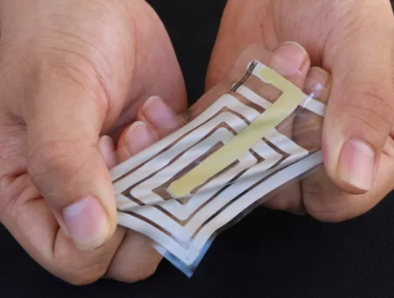
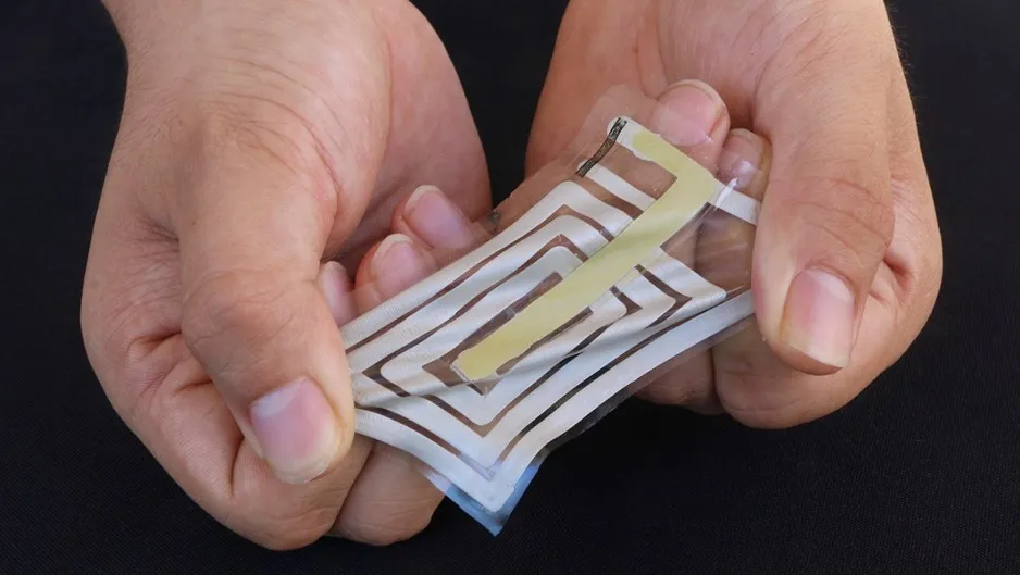
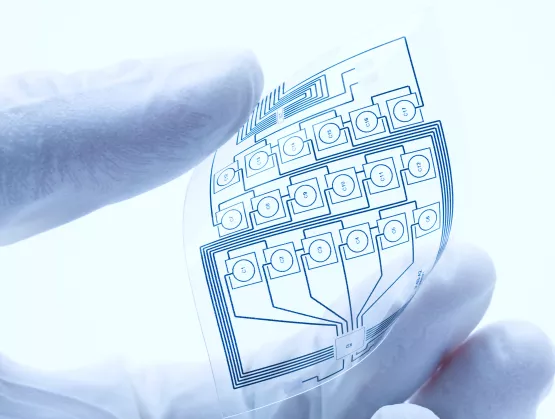
Presentations at this year’s FLEX Conference illustrated the ongoing development of manufacturing tools and processes, materials, and test and reliability evaluation techniques for the growing field of hybrid electronics, which includes printed electronics and flexible hybrid electronics (FHE). Additionally, the field includes the use of additive manufacturing processes for electronics packaging and system assembly, from die attach to flexible printed circuits.Hosted by FlexTech, a SEMI Strategic Technology Community, the conference provides an opportunity for the device making supply chain to connect to R D, design and manufacturing innovations. A review of some of the key developments highlighted in FLEX presentations follows.Innovations in Flexible Printed CircuitsTokyo-based Elephantech has been focused on using advanced inkjet systems to produce flexible printed circuits. Using additive methods instead of subtractive to produce PCBs can enable reductions in carbon footprint, copper usage and water consumption. In order to achieve these benefits, Elephantech has developed processes for combining inkjet printing of metals and electroless plating. The company synthesizes copper nano particles, which it uses to formulate metal ink. It has implemented artificial intelligence to increase print accuracy, showing the capability of average drop position error of less than 2μm, and depositing 20μm droplets into 40μm grooves and wells (Fig 1).Fig. 1. Elephantech inkjet results showing ~2μm precision and prototypes with 50μm line widthExamples of Elephantech’s use of flexible printed circuit technology include a set of switches for a curved monitor and a pressure sensor with reduced footprint and component count. The company intends to directly compete with larger, rigid PCBs, and is developing a mass-production system with 57,840 nozzles that can process sheet sizes of 500 x 830 mm.Traditional processes for component attach on PCBs include mass reflow ovens, thermal compression bonding, and spot laser reflow. Laserssel has developed laser selective reflow, which promises warpage- and damage-free bonding at increased processing speeds. In addition to improving the productivity of rigid PCB production, the laser selective reflow could also enable in-line processing of roll-to-roll flexible printed circuits, replacing the use of trays for bonding to flexible printed circuits.Scrona, which spun out from ETH Zurich, has developed MEMS-based printheads to improve electrohydrodynamic (EHD) printing. By using an electric field to pull droplets out of the print nozzle, EHD can enable much higher print resolution (sub-micron, compared to tens of microns), and enable the use of higher viscosity inks than would be possible with traditional inkjet heads. While EHD has been under development for some time, its application has been limited by crosstalk, in which the electric fields of adjacent nozzles interact with each other, and the requirement for the nozzle to be within tens of microns from the substrate to enable high print accuracy.Scrona’s MEMS-based nozzles address these EHD problems by shielding adjacent nozzles to prevent crosstalk and by creating a uniform electric acceleration field, which increases print distance to the order of a millimeter. The company has used its system to print a variety of inks on different substrates, as well as conformal printing on 3D surfaces (Fig. 2).Fig. 2. Example of printing silver wires across a polished glass edge; line pitch 25μm, glass thickness 1mmThe Rochester Institute of Technology (RIT) has been developing an additive technique called liquid metal droplet jetting, which can deposit metal traces functionally equivalent to solid wires. The process uses metal wire as a feedstock, which is a fraction of the cost of nanoparticle metals. While tin, zinc, and aluminum have been used, silver and copper are still under development. The wire is melted in a micro-crucible, which feeds a nozzle; metal droplets are then jetted on demand in an argon environment to prevent oxidation (Fig. 3, l). Upon hitting the substrate, the drops solidify into metal traces equivalent to solid wire, quickly enough to avoid melting flexible films, and without curing or drying.Several methods have been explored to eject the jets from the nozzle, including magnetohydrodynamic using electromagnetic pulses, piezo-actuated pistons, and pneumatic jetting using compressed gas (Fig. 3, r). These techniques range from high-jetting-frequency and high-cost to simple and low-cost but low-frequency. Higher frequency enables overlap of droplets, increasing conductivity, and reduced processing time.Fig. 3. Concept of liquid metal droplet jetting (l); pneumatic droplet ejection approach (r)In addition to ongoing development of deposition tools and processes, the material set for additively printed electronics continues to expand. Iris Light Technologies, which spun out of Argonne National Lab and Northwestern University, is developing photonic inks for wafer-scale production of active devices including photodetectors, LEDs, and lasers. The semiconductor-based ink can be deposited via aerosol jet onto silicon wafers. Iris Light is focused on 2D semiconductors, specifically black phosphorous, which has a wider spectral coverage than graphene, is tunable in emission and absorption, and has high mobility.An example of the broadening of the additive manufacturing supply chain, Kraetonics has developed software for creating slices to be used in designing 3D-printed structures and elements. The software enables manufacturing 3D volumetric circuits with reduced size, weight, and power compared to 2D PCBs. The process involves 3D printing of hybrid mechanical-electrical assemblies such as circuits and antennas.Innovations in Test and ReliabilityAn area of active interest in the hybrid electronics community is that of test and reliability. American Semiconductor, a developer of flexible circuitry, and Bayflex, a value-added partner of Japanese equipment company Yuasa, are conducting a project on dynamic harsh environmental FHE reliability testing. The goal is to identify root causes of FHE material and system failures.The companies are developing extended temperature and humidity tests to determine FHE system lifetimes and identify causes of failures from physically deforming FHE materials and systems in harsh temperature and humidity environments. Materials under consideration for testing include:Copper on polyimide substrate with a small outline package IC and surface-mounted componentsNobleflexTM, a multilayer substrate with gold on polyimide in development for medical devicesSilver on PET substrate, with small outline package IC.The team is soliciting other test devices and is planning to coordinate with ongoing development of FHE test standards coordinated by SEMI.Henkel reported on an investigation of accelerated temperature cycling test methods, in which the company applied different combinations of temperature range, stress, and frequency of mechanical force in an effort to reduce cycle time for testing component attach reliability. The study was able to achieve similar failure modes using an accelerated test method in the case of a bonding position shift in which cracking of the die attach film was the failure mode (Fig. 4, approach 4). The study found the greatest acceleration in the case of reduced thermal shock cycles (Fig. 4, approach 1).Fig. 4. Approaches evaluated for accelerated testing of component attach.Engineering consulting firm Exponent presented the results of a study on mechanical testing for characterizing fatigue performance of flexible electronics, conducted with continuous monitoring of fatigue for 6-pin flexible flat cables from seven different vendors. Exponent found that continuous monitoring during bending fatigue testing provided greater resolution in test results including detection of intermittent failure in each sample. The study also found that strain amplitude was a critical factor for determining fatigue life, and that flat flexible cables with larger pitches showed improved fatigue performance.About SEMI FlexTechFlexTech, a SEMI Strategic Technology Community, promotes the growth, profitability and success of the flexible hybrid electronics industry by developing educational forums, directing research, and promoting technology innovation.SEMI FlexTech members benefit from speaking and business networking opportunities, introductions to key industry players, research reports, technical funding, access to end users and industry advocacy at FLEX Conferences.Gity Samadi is Director of SEMI research and development funding programs and SEMI FlexTech and SEMI Nano-Bio Materials Consortium (NBMC). Paul Semenza is an advisor to SEMI on special projects. He was previously with NextFlex, the Flexible Hybrid Electronics Manufacturing Innovation Institute.
Read More
Since 2015, FlexTech has funded three projects with ITN Energy Systems, based in Littleton, Colorado. The projects all draw on a unique concept of using thin, flexible ceramic sheets as both a substrate for functional devices and as an integral part of the hermetic packaging to support paper-thin FHE products. Each program was increasingly sophisticated, enabling a larger variety of functions to be integrated into a common package. Independent functions such as energy storage, energy harvesting, or printed microelectronic circuits are deposited on their own ceramic substrate and the layers vertically stacked and interconnected into a monolithic structure that combines several functions in the smallest possible package volume.The ITN projects provide excellent examples of the power of collaborative research and development to help de-risk investments in next-generation electronics. All the projects were conducted with technical contributions from small and large businesses as well as university partners. The programs were funded by the U.S. Army Research Laboratories (ARL), directed by industry leaders and managed by SEMI FlexTech with the focus on utilizing the advantages of flexible hybrid and printed electronics (FHE) to create lighter-weight, lower-power, more conformable electronics than available commercially today. Markets ready to take advantage of FHE developments include healthcare, aerospace, mobility, consumer electronics, industrial electronics.ITN was founded in 1995 to focus on researching and developing technologies related to aerospace, energy and the environment for defense and commercial marketplaces. Its business model employs collaborative R D projects to explore, develop and validate promising next-generation clean energy technologies with an emphasis on tackling the manufacturing challenges that enable low-cost, high-volume production of thin-film devices on flexible substrates. Those technologies that meet the technical and business requirements of the market are commercialized via focused, spin-out companies with five such spin-outs formed so far. The work on ultra-thin batteries needed by the SEMI FlexTech community readily slid into their portfolio of projects.Project 1 – New Solid-State Lithium BatteryThe first project kicked off in 2016, with ENrG, and successfully supported the development and validation of novel Solid-State Lithium Battery (SSLB) products with total packaged thickness ranging from 50-250 microns. The SSLB proved to have substantial advantages in form factor and performance when compared with both commercial-off-the-shelf batteries and emerging technologies. For example, the SSLB provided more than double the operating time in a substantially smaller package in powering an audio device supplied by SEMI FlexTech partner companies.By avoiding the use of liquid electrolytes, the ITN SSLB also eliminates flammability issues while still allowing the benefits of lithium-based battery chemistry. The SSLB boasted many attributes attractive to the FlexTech community, including: Ultra-thin form factor, i.e. 250 microns thick, mAh class packaged batteries High volumetric energy density, i.e. baseline products with ~500 Wh/l and a roadmap to 1,000Wh/l The ability to support high current pulsing, i.e. current pulses at 4-10C rates, in support of demanding FHE duty cycles High temperature compatibility with solder reflow and other FHE integration schemes Rechargeability with high capacity retention at 1,000 cycles This new SSLB has formed the foundation of subsequent projects and commercialization efforts.Project 2 – Adding Energy Harvesting Based Recharging Capability The second SEMI FlexTech-funded project proposed a novel self-recharging battery with the addition of Lucintech’s cadmium telluride (CdTe) photovoltaics (PV), which was also deposited on thin yttria stabilized zirconia (YSZ) substrates. Because the CdTe supports a superstrate configuration, the SSLB can function as the back sheet for the PV package, thereby dramatically decreasing overall package thickness. The resulting flexible integrated power pack provided up to 0.25 Wh of energy storage and ~0.2 W of PV generating capacity in a total package less than 250 microns.As part of that effort, the ITN Team identified an effective power-management circuit that was ultimately compatible with die thinning and form factors very attractive to FHE. Consequently, the PV and SSLB were interconnected into a common power bus that enabled FHE to be operated with either the PV, SSLB or some combination of the two.ITN is seeing great interest in this product and both developing a version with substantially higher capacities than the project entertained for a UAV platform while ramping to low volume with support from NextFlex, a member of the Manufacturing USA network, and formed in 2015 through a cooperative agreement between the U.S. Department of Defense (DoD) and FlexTech Alliance.Monolithic integration of function layers atop of SSLB for high performance microelectronics device Project 3 – Integration with Processing and Sensor SystemsThe third FlexTech-funded project builds further on that foundation. In this project, the ITN Team is maturing the technologies to create a battery with an integrated processing and sensor system, nicknamed BiPASS. In addition to SSLB layers, the BiPASS package integrates printed circuits on YSZ employing high-performance, silicon- based bare die micro-electronics and/or thin film sensors into the common packaging. Mock-up of the charge control circuit on SSLB The initial demonstration integrates a commercial lithium battery charge control circuit within the SSLB packaging to create a monolithically integrated power module. There have also been promising developments of the University of Rhode Island’s metal oxide (MOx)-based thin film gas sensors that have dramatically increased sensitivity when deposited on thin YSZ. The resultant sensor achieves ppb detection of trace explosives gases that can be powered by SSLB. Along the way, ITN’s partners Molex and SunRay Scientific matured several aspects of FHE circuit printing and integration on both PET and YSZ, including new materials and processes for conductive traces, and bare die attachment with fine features. The project is in its final stages and the ITN Team now has a promising roadmap to integrate power, microelectronics, and thin film sensors/sensor systems into a single paper-thin package.Commercial Scale-Up StrategySince the initial demonstrations were completed, ITN has been actively maturing a commercial scale-up strategy based on significant market-pull and interest from several companies. A new venture to commercialize this next generation SSLB is in process. As part of those discussions, ITN is in active discussions with potential strategic partners to support the transition to high-volume production to access additional markets, many of which are cost-sensitive and need a higher degree of production maturity.In the meantime, ITN’s limited volume SSLB production line is already supporting medical device customers. In addition, a baseline SSLB (~2.5 mAh capacity) has been developed and tested in several new applications, including wearables, sensors and smart labels.“Based on the acceptance of these project in the market, I believe all three projects have provided significant value to the SEMI FlexTech community,” noted Brian Berland, Chief Technology Officer at ITN. “In addition, the connections and visibility we have gained within the industry by partnering with SEMI FlexTech have been invaluable. We are excited to continue this journey with new and additional projects. In the meantime, we are hopeful that our ongoing discussions with investment partners will support our commercializing of these components.”For more information visit www.flextech.org. SEMI FlexTech is currently (from 6/10/2020 – 7/17/2020) accepting white papers for new technology development projects. Read more at www.flextech.org.About the AuthorDr. Gity Samadi is the SEMI FlexTech Program Manager. Gity is responsible for the flexible hybrid electronics R D consortium activities including project awards and management, Technical Advisory Council management, and webinar/industry event planning for the building and fostering of this dynamic innovative community.
Read More
Thanks to developments in science and technology, artificial intelligence (AI), cloud computing, big data and other technologies have been used to establish smart healthcare systems that helps societies respond more effectively to disease outbreaks. The spread of novel coronavirus starting in late 2019 has revealed how not only traditional medicine but also Smart MedTech applications can be instrumental on the anti-epidemic front lines.To give updates on the development of Smart MedTech and how it shines during the fight against COVID-19, SEMI invited Dr. Pei-Yuan Lee, Honorary Superintendent of Show Chwan Memorial Hospital, to share with MSIG (MEMS Sensors Industry Group) and Flex-Tech members how the international community and Taiwan are bringing their best in Smart MedTech to the table and how their collective efforts are helping tackle COVID-19 challenges.Taiwan’s COVID-19 rapid screening reagents and antibody testing help curb coronavirus transmissions Taiwan’s medical community has demonstrated its prowess in responding to the COVID-19 outbreak. Using its nucleic acid extraction reagent, Taiwan Advanced Nanotech Inc. tested 128 specimens from passengers aboard the SuperStar Aquarius cruise ship in only eight hours in early February. Taiwan’s leading research institute Academia Sinica successfully synthesized the first group of monoclonal antibodies capable of recognizing the new coronavirus protein on March 8, enabling testing to be completed in 15 minutes. The College of Medicine of National Taiwan University announced on March 27 that its 30-second screening device had helped identify asymptomatic carriers. The devices detect COVID-19 in people with no symptoms if they have pulmonary infiltration and edema. It took only 14 days for Academia Sinica to successfully synthesized the first group of monoclonal antibodies capable of recognizing the new coronavirus protein. On April 22, three biomedical companies in Taiwan launched a COVID-19 test that produces results from samples of patient mucus in less than 10 minutes to greatly enhance testing speed. Once the test method is approved by the Taiwan government, it will take Taiwan’s medical strategy against COVID-19 to the next level.Artificial Intelligence: the key to upgrading traditional healthcare practicesAI is a key enabler of the transition from traditional medical practice to Smart MedTech. To help fight the COVID-19 outbreak, a National Cheng Kung University medical team developed a 30-minute coronavirus testing procedure that uses AI to read pulmonary X-ray images and automate medical records. Taiwan AI Labs leveraged AI to simulate how drug molecules combine with viruses to reduce research time by three to four years. AI ​​diagnostic technology from the Alibaba DAMO Academy (Academy for Discovery, Adventure, Momentum and Outlook) and Alibaba Cloud interprets CT images of COVID-19 patients with 96 percent accuracy in 20 seconds. AI-powered algorithms improve diagnostic test accuracy, allowing clinicians to quickly analyze scans of pulmonary lesions and quantify the severity of lung damage.Startups have also joined the fight against COVID-19. Taiwan's Internet of Things (IoT) startup iWEECARE invented the world's smallest smart thermometer patch. Heroic-Faith Medical Science launched a device that uses IoT and AI to monitor lung sounds. With Smart MedTech expected to be fertile ground for future venture investments, enterprises must find their niches in establishing new technologies in a much more systemic way. Taiwan startup Health-Faith Medical Science developed a respiratory diagnostics device that uses IoT and AI technology to monitor chest sounds in real time. Anti-epidemic technology to help fulfill smart medtech vision Many AI and big data technologies previously deployed in hospitals and healthcare systems are helping regions around the world speed their pandemic response. The United States and China have started to develop facial mask recognition systems powered by AI, while a team in the Department of Bioinformatics and Medical Engineering at Asia University has devised a facial recognition system combining IoT and AI technology with infrared thermal imaging cameras. At Johns Hopkins University, the Center for Systems Science and Engineering is using AI to create big data models that track global cases, people and traffic flow, and other variables for real-time data analysis that enables epidemiologists to more accurately predict COVID-19 transmission paths. Graphen, Inc., a New York-based provider of next-generation AI platforms, launched the world's first AI COVID-19 genetic evolutionary path analysis systems to gauge the virus’s transmission route and accelerate pandemic response. Both the United States and China are also using robots and drones to improve epidemic research and patient treatment. For the first confirmed case in the United States, robots were used to assist with medical care. In China, robots facilitate deliveries of disinfectants to makeshift hospitals built to expand the nation’s capacity to treat COVID-19 patients. While Taiwan’s robots are traditionally used for hospitality, transportation and disinfection purposes, future robotics research and development will focus more on medical applications that shift more work from medical staff to technology. With abundant technological resources and expertise, Taiwan can join hands with the rest of the world to combat the COVID-19 pandemic. Emerging technologies are pointing the way toward a new paradigm for healthcare community. Biotech, artificial intelligence, and robotics have given rise to new applications that increase virus screening accuracy and efficiency. This growing wave of technological defenses against the pandemic will become a long-term force for stability and strength in healthcare systems across the world.To get involved in SEMI Taiwan Smart MedTech Community, please contact Helen Chen, Outreach Manager, at [email protected] Huang and Winnie Chang are marketing and public relations specialists at SEMI Taiwan.
Read More
As the body’s largest organ, skin is responsible for the transduction of a vast amount of information. This conformable, stretchable, self-healable and biodegradable material simultaneously collects signals from external stimuli, which translates into information such as pressure, pain and temperature. The development of electronic materials, inspired by the complexity of this organ, offers a tremendous unrealized materials’ challenge. Fortunately, the advent of organic-based electronic materials may offer a solution to this longstanding problem.Zhenan Bao, K.K. Lee Professor of Chemical Engineering, Stanford University, is one of the world’s leading researchers working on the design of organic electronic materials that mimic skin functions. SEMI’s Maria Vetrano interviewed professor Bao to preview her February 25 keynote, Skin-Inspired Electronics, at FLEX|MEMS Sensors Technical Congress (MSTC) 2020, February 24-27, 2020, at the DoubleTree by Hilton in San Jose, California.Join us at FLEX|MSTC to meet Professor Bao and other industry influencers furthering innovation in flexible hybrid electronics (FHE) and MEMS sensors. Register now to connect with her at FLEX|MSTC or visit her on LinkedIn.SEMI: Your pioneering work on the use of electronic materials to construct second skin is a major step forward in human-machine interfaces. Could you please describe second skin?Bao: Second skin is a new electronic-device platform encompassing electronic devices that have skin-like properties such as stretchability, self‐healing ability, biocompatibility and biodegradability. In essence, the second skin is an electronic system of fully integrated multifunctional components operating on the surface of or inside the body to enable smart healthcare for disease prevention and treatment and to enhance the functional capabilities of natural skin. The second skin could also serve as a module to connect our human body to the Internet, thereby allowing human integration with the Internet of Things (IoT) for next‐generation wireless communications. In this way, we can view the second skin as an artificial body part that can be used to improve our everyday lives.SEMI: How might second skin operate in the human body?Bao: It has many potential uses. It could be a prosthesis for people who have lost their sense of touch. It could be used to repair damaged skin as well as to provide enhanced functionality that’s not possible with biological human skin. It could, for example, connect us with our external environment, with other people, even with our cars.I can also envision second skin as an implantable device for both neurostimulation and for early detection of disease. Schematic illustration of structure of second skin composed of functional devices: sensor, integrated circuit, display and power supply. Source: Stanford University SEMI: How did you get started in this research? Bao: Sixteen years ago when I started at Stanford, I learned of a colleague in mechanical engineering who was working on robotic cockroaches. That’s when I understood the need for sensor functions in robotics.I considered the large number of people with prosthetics who do not have a sense of touch. With this audience in mind, I started by designing a simple flexible electronic device that could take the shape of skin, even conforming to a robot hand, thereby approximating the natural sense of human touch.Once we developed the first sensor, and realized that its touch sensitivity could eclipse that of human touch, I asked myself: what can we learn from second skin – in addition to its sensing functionality?Skin is not just flexible; it is biodegradable and stretchable. So we started to dream. We began by developing electronic materials, either conductors or semiconductors. We added new functionality, such as self-healing properties, biodegradability and stretchability. That opened the way to new materials’ development.SEMI: What discoveries have you made in new materials?Bao: Over the past decade, we’ve developed skin-like materials with electronic properties that are on par with the best conducting and semiconducting polymers. Some of our skin-like semiconducting polymers can perform even better than amorphous silicon. That means with suitable processing methods, we can make stretchable ICs, initially with tens of transistors that can perform analog or digital functions, and in a later stage, stretchable displays driven by active matrix arrays.SEMI: What would it take to put these materials into production?Bao: We need to develop methods to pattern the skin-like electronic materials into fine features. We have been leveraging similar processes used for flexible circuit boards. Some research groups are developing roll-to-roll fabrication and printing methods.SEMI: Which technologies/applications are you commercializing?Bao: C3Nano is a Bao Research Group spin-off startup that is commercializing nanomaterials that are promising for bendable and foldable electronics.Another spin-off that is licensing our technology, PyrAmes, is developing a continuously non-invasive blood-pressure monitor. It’s not a cuff so the patient doesn’t have to remember to put it on.In the shorter term, we’re looking at putting artificial skin on prosthetic limbs and robotic hands. Further down the road, we could put skin on wounded regions of the body, forging connections to nerves that would support realistic sensation.To realize these applications, we’ll need to conduct further R D on materials and applications. The manufacturing of these devices still needs much more development.Fortunately, we’re part of a fertile development ecosystem at Stanford. I started the Stanford Wearable Electronics Initiative (eWEAR) to forge collaborations across Stanford campus as well as with industry.SEMI: What would you like FLEX|MSTC attendees to take away from your presentation?Bao: I’d like them to realize that the future of electronics is changing. I imagine a future in which the functions of a smartphone will disappear into what we wear, what we attach to our skin and what we implant inside our body. I believe that skin-like electronics will help to facilitate this future, allowing us to connect with each other and our surroundings in ways that feel natural, yet that also enhance our quality of life. Zhenan Bao is K.K. Lee Professor of Chemical Engineering with courtesy appointments in Chemistry and Material Science and Engineering at Stanford University. She founded the Stanford Wearable Electronics Initiate (eWEAR) and serves as the faculty director. Prior to joining Stanford in 2004, she was a Distinguished Member of Technical Staff at Bell Labs, Lucent Technologies from 1995 to 2004.Bao has over 500 refereed publications and over 65 U.S. patents with a Google Scholar H-Index 155. In her recent work, she has developed skin-inspired organic electronic materials, which have resulted in unprecedented performance or functions in medical devices, energy storage and environmental applications. She has pioneered several important design concepts for organic electronic materials. Her work has enabled flexible electronic circuits and displays.For more information on professor Bao’s research, visit Bao Research Group. FLEX|MSTC is organized MEMS Sensors Industry Group (MSIG) and FlexTech, SEMI technology communities focused on the growth of MEMS sensors and the flexible electronics supply chain, respectively. Maria Vetrano is a public relations consultant at SEMI.
Read More
MEMS technology has changed human interaction with electronic devices. Introduced in the 1990s, the first mass-market MEMS devices were used for inkjet printheads and automotive airbag crash sensors. Today, MEMS are ubiquitous, with billions of the tiny devices adding intelligence and interactivity to smartphones, smart speakers, wearables, automobiles, biomedical devices, remote monitoring and event detection systems, and countless other applications. Integrating MEMS with Flexible Hybrid Electronics (FHE) is an important step in the evolution of this miniaturized intelligent sensing technology, paving the way for its use in new classes of flexible, conformal devices.The integration of the two technologies promises to breed new applications in small form factors but also presents challenges inherent to FHE design and fabrication processes. SEMI’s Nishita Rao caught up with Nathan Pretorius, prototyping and automation engineer, NextFlex, to discuss MEMS-FHE device integration challenges and opportunities ahead of his February 26 presentation, Integrating MEMS Devices in FHE, at FLEX|MEMS Sensors Technical Congress (MSTC) 2020, February 24-27, 2020, at the DoubleTree by Hilton in San Jose, California.Join us at FLEX|MSTC to meet Nathan and other industry influencers advancing innovation in FHE and MEMS sensors. Register now to connect with him at FLEX|MSTC or visit him on LinkedIn.SEMI: Why is integrating MEMS devices into FHE systems important? What new use cases might it enable?Pretorius: The main value proposition of integrating MEMS devices into FHE is that it allows MEMS devices to exist in a different form factor than was possible previously, giving us high-quality MEMS sensors on the flexible and conformable platform of FHE.Ease of application, flexibility, lower cost and rapid iteration on a design are just some of the benefits of FHE devices. And because there are few robust FHE sensors that overlap with MEMS’ capabilities, when you combine the two, you get a lot of compelling uses. That’s why NextFlex is working with agencies and companies to evaluate MEMS’ integration, including using bare MEMS die with microfluidics and promoting new ways of attaching and packaging MEMS die for use with FHE. SEMI: Why is FHE an ideal platform for integrating various types of sensors?Pretorius: MEMS integrated with FHE devices are ideal for rapid design and deployment of data-gathering sensor nodes — which we can iterate for specific applications. A few examples include on-body health monitoring devices for bio-fluids analysis, medical pressure sensors for monitoring blood pressure, and peel-and-stick sensors nodes for infrastructure monitoring. In terms of design and production, FHE devices support rapid prototyping, allowing for instantaneous design-iteration cycles. This speeds design-to-production over traditional rigid PCBs and copper flex because the feedback cycle time between design, manufacturing and testing is shorter, accelerating time to market. What’s exciting about FHE technology is that a variety of sensors or components, including MEMS, can be designed into the base system to easily customize it for a specific application. In addition, our experience shows that when compared to a traditional rigid PCB, an FHE board reduces manufacturing steps and device weight by two-thirds and, perhaps most importantly, converts the device to a thin, conformal shape that makes possible products in new form factors. SEMI: What are the primary challenges to integrating MEMS with FHE? What is NextFlex doing to help device manufacturers address these challenges? Pretorius: There are a few challenges, some of which are device-specific. Most recently, I’ve been focusing on inertial and timing devices, including accelerometers, gyroscopes and resonators. There are a few technical challenges involved in the process of getting the devices from the wafer to an FHE substrate. The wafer processing is very important, especially the dicing and thinning steps. After thinning and dicing, the die is placed onto the FHE substrate. The stresses caused by bonding to the substrate have to be understood and characterized. After placing the die, you then have a calibration step, which is normally performed after the device is packaged. With a MEMS die placed onto directly onto an FHE substrate, calibration then must be done.Finally, the device encapsulation is important, since on an FHE substrate the hard-to-soft material transition is very important to mitigate stresses to rigid component interfaces. We have also been looking at how to work with devices that have damping vents. Flexible encapsulants are inherently more permeable to gases and water vapor than hard encapsulants, so studying the encapsulation of MEMS devices on FHE is another area of interest. NextFlex has been working in a supporting role to evaluate best design practices and best attach and integration methods. In addition to our ongoing collaborative programs, NextFlex is developing the FHE manufacturing ecosystem to include system and component manufacturers and designers, product developers, and materials and equipment providers.SEMI: How do we facilitate closer collaboration between the FHE manufacturing ecosystem and MEMS suppliers such as MEMS device manufacturers, product developers, and materials and equipment providers?Pretorius: It’s important to include manufacturers early in the design process so we can identify challenges up front. That’s why NextFlex spearheads technology road-mapping efforts that include representatives from across the manufacturing ecosystem. We use the roadmaps to prioritize challenges that we can address effectively through collaboration, focusing the industry on solving problems through Project Calls that reveal integration challenges and results from real devices and that tell us how the materials and equipment actually perform with a real device.NextFlex keeps the information flowing, holding quarterly project update webinars to share results. As current devices are optimized for the process in which they will be used, we learn a lot from the project performers who make FHE system demonstrators — and we share that information with the member community. SEMI: Can you point to an example of a successful MEMS-FHE device integration?Pretorius: MEMS-FHE integration is still in the early stages, but we are working on several projects including a DARPA Seedling project for which we have integrated MEMS sensors into FHE systems for testing and evaluation. We plan to continue this work by integrating MEMS and FHE devices using methods that support mass production.SEMI: What would you like FLEX|MSTC attendees to take away from your presentation?Pretorius: We would like to see the FHE community work more closely with MEMS device manufacturers. For example, NextFlex often works with manufacturers to gain access to bare die, which is still a significant hurdle in making devices.The best way to speed things along is to get involved. We encourage FLEX|MSTC attendees to join NextFlex. As a prototyping and automation engineer at NextFlex, Nathan Pretorius explores new print methods for prototyping and automation using novel materials and processes. Pretorius currently focuses on how best to apply software scripting and machine learning to streamline FHE processes. Prior to joining NextFlex, he researched the strengths of roll to roll and screen printing on printed electronics designs, including capacitive touch interfaces, FHE passive component design, and antennas. Nathan holds a Bachelor of Science degree in Graphic Communications from Clemson University. FLEX|MSTC is organized MEMS Sensors Industry Group (MSIG) and FlexTech, SEMI technology communities focused on the growth of MEMS sensors and the flexible electronics supply chain, respectively.Nishita Rao is marketing manager for technology communities at SEMI.
Read More
VTT Technical Research Centre of Finland Ltd (VTT) has its sights set high. As a leading global research and development firm , VTT is out to produce bio-interfacing and biodegradable flexible hybrid electronics (FHE) devices that help tackle some of the world’s greatest challenges including environmental degradation and food scarcity.SEMI’s Maria Vetrano interviewed Antti Vasara, president and CEO of VTT Technical Research Centre of Finland, to preview his February 25 keynote, Beyond Flexible Hybrid Electronics: Biodegradable Electronics and Interfacing Bio+Electronics, at FLEX|MEMS Sensors Technical Congress (MSTC) 2020, February 24-27 at the DoubleTree by Hilton in San Jose, California. Join us at FLEX|MSTC to meet Antti and other industry influencers driving innovation in flexible hybrid electronics (FHE) and MEMS sensors. Register now to connect with him at FLEX|MSTC or visit him on LinkedIn.SEMI: What is body-interfacing electronics and what is your vision for bio-interfacing and biodegradable electronics?Vasara: Body-interfacing electronics have existed for decades. Developed in the 1970s, the wireless heart rate monitor is a good example. While continuous heart monitoring with a compact, inexpensive wearable device is widely accessible technology, other bodily parameters, such as cholesterol levels or biomarkers, are diagnosed every time we see a doctor. Establishing a baseline using multiple measurements — before symptoms develop is actually much more effective.That’s where bio-interfacing comes in. Bio-interfacing devices will continuously measure and analyze complex biogenic substances such as sweat, breath, blood and urine. A smart patch for continuous sweat monitoring, for example, would overcome several challenges: supporting electronics functionality in liquid environments, managing the transport of harvested samples to and from the sensor, managing potential contamination, and disposing of samples after measurement.While FHE in principle delivers the right building blocks and is an ideal form factor for a wearable sweat analytics patch, flexible circuits are not ready for out-of-the box interaction with biological matrices. Hence, our mission at VTT is to anticipate and develop the upscaling process know-how required for FHE devices that either interface with biological systems — or that must themselves biodegrade.We’re also focusing on biodegradable electronics because environmentally conscious end-users and manufacturing companies want biodegradable versions of energy-autonomous, label- or sticker-like Internet of Things (IoT) sensors. Typically used for packaging, logistics, environmental monitoring and medical diagnostics applications, these sensors — which have a lifetime of a few days, weeks or months — have become very popular. Unless they are biodegradable, however, they just add to landfill.SEMI: What approaches is VTT using to develop bio-interfacing and biodegradable electronics?Vasara: In our Business Finland-funded ECOtronics project, we are working with our partners to create recyclable and compostable electronics and optics that use renewable resources. For example, devices developed using substrate materials like paper, cardboard or VTT’s in-house-developed nanocellulose films and biopolymer films for environmental monitoring or skin patches can be easily recycled or even biodegrade naturally. Where possible, we use roll-to-roll printing to generate the device circuitry, and on a component level, we have optimized our assembly process towards bare-die component bonding to reduce the overall footprint of non-biodegradable waste per device.SEMI: What use cases do you find most promising and why?Vasara: A prominent example of a single-use test that generates a large amount of waste is the digital pregnancy test. When breaking it down into components, you will find a rigid circuit board with microprocessor, a couple of coin cell batteries, a liquid crystal display, a LED light source and photodiode, and a large chunk of plastic packaging around it. The materials and battery capacity of such a device would be sufficient to run hundreds of pregnancy tests – actually technical overkill.By using printed circuits on biodegradable substrates, bare-die assembled components (ASIC, LED light sources, photo diodes, thin film batteries as power sources) and device packaging composed of biodegradable plastics, we can completely redefine the environmental footprint of single-use tests. We are currently developing a toolbox for our customers to turn their existing conventional test into an ecotronic form factor.Another exciting use case is a sweat sensor that we developed collaboratively with Ali Javey, Ph.D., professor of Electrical Engineering and Computer Sciences, UC Berkeley, and the co-director of Berkeley Sensor and Actuator Center (BSAC). Together with his team, we created a wearable electrochemical sensor for continuous sweat analysis during exercise. With the UC Berkeley group providing the chemistry to monitor N+, K+ ion and hydration levels in sweat over the duration of several hours, VTT delivered the underlying sensor platform, featuring the printed sensor electrodes and sweat harvesting microfluidic channels for fluid management and transport. It’s exciting to see what we can achieve by combining techniques from different disciplines, in this case electrochemistry, printing, packaging and microelectronics.SEMI: How can industry enable the development/manufacture of flexible FHE devices? Where does VTT fit into the ecosystem?Vasara: As many FHE devices target large-volume markets, scalability of manufacturing is key: How can I get from one device (= working prototype) to a handful of devices (= feasibility study), to thousands (= pilot manufacturing), to a million (= mass manufacturing) without compromising the quality of the system’s performance and reliability?Access to upscaling infrastructure is essential for the development of novel FHE devices and methods, but infrastructure is expensive. That’s where our establishment of a roll-to-roll pilot printing line to bridge the gap between laboratory R D and mass manufacturing has proved invaluable. We can provide a unique worldwide upscaling infrastructure for advanced FHE devices, with a strong focus on large-area roll-to-roll processes and hybrid assembly. This service removes our customers’ burden of high infrastructure investment in early development stages and it allows us to guide customers along their development path, from prototype to mass production.Watch our video: VTT pilot manufacturing for diagnostics and wearablesSEMI: Is there anything else that device manufacturers need to know in order to succeed?Vasara: In my eyes, the success of FHE devices eventually depends on several factors: It requires a high degree of automation, well-optimized processes, reliable supply chains, and perhaps most importantly, clear standards and rules for designers to guarantee flawless interoperability of all the different elements on a flexible and hybrid circuit. Let us not forget – we are trying to marry electronics with printing, biology, packaging, microfluidics, injection molding and other fields of expertise.We recently finalized the compilation of a set of design rules for publication in our state-of-the-art overview of printed and hybrid electronics manufacturing methods. You can download the overview, PrintoCent Handbook, for free.SEMI: What would you like FLEX|MSTC attendees to take away from your presentation?Vasara: The latest technologies and innovations in microelectronics, MEMS, printing, materials, and biosensors provide us a toolbox for true innovation in the FHE space. Now we need cross-disciplinary thinking and daring steps to combine different manufacturing methods and skill-sets. The ideal cross-disciplinary team might include: The printing engineer who knows how to design contact pads for a bare-die IC assembly The biologist who knows about the thermal and mechanical stress in a printing environment to design processes for bio-functionalization of surfaces The electronics engineer who knows how to optimize a circuit powered with an enzymatic biofuel cell The number of sensors deployed on (or inside) our body, in our drinking water, in our cars, on our fields, in our pets, and everyday products will surely grow. Let us make sure they leave the smallest environmental footprint possible.Antti Vasara, Ph.D. has been the president and CEO of VTT Ltd since 2015. VTT is a visionary research, development and innovation partner with over 2000 people and a turnover exceeding 250M EURO. Vasara is president of EARTO (European Association of Research and Technology Organisations) and is chairman of the board of Palta (Finnish Service Sector Employers). In addition, he is a non-executive director of Elisa Oyj (largest communications operator in Finland) and a board member at EK (Finnish Confederation of Industries).He has served on several high-profile groups on industrial and innovation policy of the European Commission, in addition to several groups in Finland on artificial intelligence and research policy. Previously, Vasara spent close to 25 years in private industry, working at Nokia, Tieto, SmartTrust and McKinsey Company. Earlier in his career, he was a researcher in optical communications with 20+ peer-reviewed articles and one international patent. Vasara holds a Doctor of Science (Technology) degree from Aalto University in Finland.For more information about VTT’s work in bio-interfacing and biodegradable FHE devices, visit VTT Research. FLEX|MSTC is organized MEMS Sensors Industry Group (MSIG) and FlexTech, SEMI technology communities focused on the growth of MEMS sensors and the flexible electronics supply chain, respectively.Maria Vetrano is a public relations consultant at SEMI.
Read More
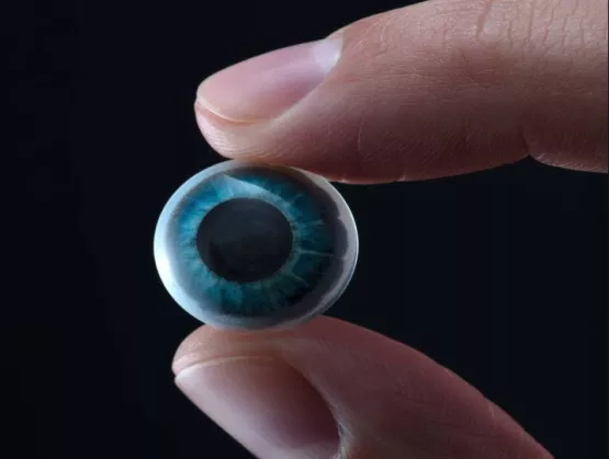
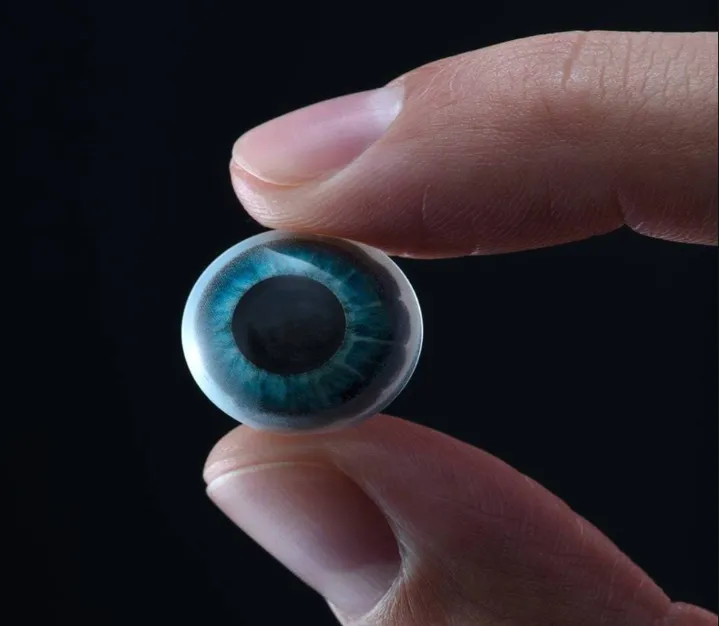
Today’s mobile devices are smaller, more power-efficient, and have more capability than we could have imagined just a decade ago. Offering ever-increasing levels of user functionality, mobile devices are now ubiquitous, and are rapidly becoming the primary mechanisms through which we interact with the digital world, our physical environment, and one another. An unintended side effect of our dependence on the current crop of mobile devices is that they are driving us to distraction.A major industry dynamic will shake things up for the better. Sensors are getting smaller and more efficient, and they’re offering attractive new functionality, giving us the ability to monitor our air and water quality, assess potential toxins in our food sources, and analyze personal health conditions, to name a few use cases. At the same time, the realization of flexible hybrid electronics (FHE) through new materials and production processes, better integration with other electronic components, more efficient energy production and consumption, and pervasive wireless connectivity are fueling the next generation of devices and experiences. What can we expect from tomorrow’s mobile devices — and how can we manage them, instead of having them manage us?SEMI’s Nishita Rao caught up with Mike Wiemer, Ph.D., VP of Engineering, CTO and co-founder, Mojo Vision, to preview his February 25 keynote, The Art of the Possible, at FLEX|MEMS Sensors Technical Congress (MSTC) 2020, February 24-27 at the DoubleTree by Hilton in San Jose, California.Join us at FLEX|MSTC to meet Mike and other industry influencers advancing innovation in FHE and MEMS sensors. Register now to connect with him at FLEX|MSTC or visit him on LinkedIn.SEMI: Mojo Vision has conducted its own research on human interaction with mobile devices. Why is this important?Wiemer: Our mobile devices have given us access to the information we need and want, improving many aspects of our lives. But our devices have also influenced our relationships and attention to our environment in negative ways. We believe that the next mobile computing platform must improve this situation. Instead of pulling us away from the moment, our devices need to embrace more human-centric engagement while still letting us access information that improves our quality of life. Mojo Vision has worked to understand this problem through our own studies and research so we can better develop an approach to address it. SEMI: How are key technical trends driving size, efficiency and capability advancements in mobile devices?Wiemer: Tiny low-power sensors are enabling ever-smaller feature-rich mobile devices that run longer on a battery charge. Smartwatches are a good example. Just a few years ago, smartwatches were not that much more than small screens on our wrists. Today, we have GPS, EKG/health monitoring, and cellular wireless interfaces all inside the same form factor.As this trend continues, we at Mojo Vision predict that our devices will continue to shrink and become even more personal: They’ll be more continuously worn and matched to our own needs and behaviors. This trend towards invisible personal devices is something we’re trying to accomplish with our solutions at Mojo Vision.SEMI: What is Mojo Vision’s concept of “Invisible Computing?” Wiemer: Our vision of Invisible Computing is based on the idea that our wearable devices should be invisible to those around us, encouraging more human interactions. These wearables should be invisible and unobtrusive to users themselves. Our Mojo Lens, which contains a full display and sensors housed inside a contact lens platform, exemplifies this vision. Using proprietary microelectronics and the world’s densest microdisplay to layer digital images and information seamlessly, Mojo Lens is redefining augmented reality. Our mobile devices today continue to increase the quantity and magnitude of interruptions. We think that shouldn’t happen. As a socially invisible device that delivers contextual, relevant content, the Mojo Lens lets us go about our daily lives, naturally interacting with other people while simultaneously enjoying the benefits of augmented reality. We think Invisible Computing can change our relationship with our devices, as well as seemingly give us superpowers. For more information, download the Mojo Vision report, Device Distraction: Understanding the Problem, Re-Thinking the Solution.SEMI: Can you tell us more about Mojo Lens?Wiemer: At its foundation, Mojo Lens is a nanoLED display, radio and sensor platform, integrated using flex technologies, and placed on your eye to provide important information. Mojo Lens can elevate or suppress this information to decrease reliance on your other devices.Unlike your smartwatch or smartphone, which react to you in a binary manner because they don’t have enough information to make autonomous decisions, Mojo Lens understands the context of your experience. That’s because it’s based on our Invisible Computing platform, which can understand your activity. Mojo Lens recognizes if you’re engaged in a conversation, driving or having a coffee, and it reacts with information accordingly.Mojo Lens could act like a real-time interpreter, for example. When someone speaks to me in a language I don’t understand, I should see “subtitles.” Or if I’m having a conversation with someone, Mojo Lens wouldn’t interrupt me with a notification at that moment. For the 92% of Americans who are interrupted by their devices during conversations every day, this prioritization can boost productivity. More importantly, it can improve the quality of our connections with the people around us.Mojo Vision’s microLED platform offers a world-record pixel pitch of over 14,000ppi and pixel density of over 200Mppi², making it the smallest, densest display for dynamic — or moving — content. SEMI: What would you like FLEX|MSTC attendees to take away from your presentation?Wiemer: It feels like the speed at which people are defining important problems and tackling them is increasing every year. And there are so many important problems to solve: space travel, autonomous driving, electric vehicles, alternative energy, quantum computing, lifespan extension, increased food production, brain-computer interfaces, AR/VR. All these problems seem impossible and “crazy,” until some group of people comes along to put a framework in place that can address them. Interestingly, these frameworks aren’t necessarily new. Rather, they build upon existing technologies and capabilities.MEMS sensors and FHE are good examples. From smart textiles, flexible displays and biological sensors to miniature radars, MEMS sensors and FHE technologies are essential building blocks. Many of the big problems we can imagine today will be solved by stacking today’s MEMs and FHE technologies in imaginative new ways. So what do we do next? I’d like to encourage FLEX|MSTC attendees to first define the problem to solve and then define the technology — rather than starting with the technology solution. Mike Weimer is a serial entrepreneur and proven science and technology leader in complex systems development and integration. Before co-founding Mojo Vision as CTO, Weimer co-founded and served as president at Solar Junction, a high-efficiency solar cell company (acquired) where he and his team set two world records for the highest-efficiency solar cells ever made by humans.After Solar Junction, Wiemer joined New Enterprise Associates (NEA) as an Entrepreneur in Residence where he sourced new investments and helped portfolio companies to develop their business and funding strategies. He is a board director at Stratio Corporation and an advisor at Stanford’s StartX Accelerator. He holds a B.S., M.S., and Ph.D. in Electrical Engineering from Stanford University.For more information, visit Mojo Vision.Interested in engaging with the MEMS sensors supply chain? MEMS Sensors Industry Group is a SEMI technology community that enables professionals in the MEMS and sensors industry to accelerate business results by addressing common challenges and opportunities.Nishita Rao is marketing manager for technology communities at SEMI.
Read More