downloadGroupGroupnoun_press release_995423_000000 copyGroupnoun_Feed_96767_000000Group 19noun_pictures_1817522_000000Member company iconResource item iconStore item iconGroup 19Group 19noun_Photo_2085192_000000 Copynoun_presentation_2096081_000000Group 19Group Copy 7noun_webinar_692730_000000Path
Skip to main content
Default Banner Image

Artificial Intelligence

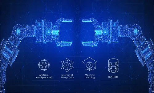
Ride the Wave of Smarter Manufacturing The year 2020 sparked a tremendous acceleration in the digital transformation worldwide, driving a sharp rise in demand for semiconductors and escalating pressure on chip factories to reduce manual functions on the shop floor. The mindset of the semiconductor industry saw a remarkable shift as it recognized with heightened urgency the need to deploy data-driven visualization, analysis, scheduling and dispatching solutions to increase automation to improve production speed and efficiency. Amidst the new excitement around Industry 4.0, chip manufacturers are rapidly deploying new technologies including IIoT, big data, machine learning and Autonomous Intelligent Vehicles (AIVs). Yet for many chip manufacturers, the path to building a smart factory is far from clear because they lack an overall digital transformation strategy. Smart manufacturing is a broad concept covering an array of technologies and solutions, making a holistic, mid- to long-term digitalization strategy rooted in the overall business strategy crucial. There are no shortcuts that can move a manufacturer instantly to Industry 4.0. Instead, this transformation is a step-by-step undertaking with a natural evolution. Some Factory Tasks Must Remain Manual – For Now The semiconductor industry has reached a point where manual processes are no longer efficient enough to support mass chip customization and remote operations. The many technological and standardization advances behind automation can help streamline some of a factory’s most labor-intensive tasks including the loading or unloading of machines or lot tracking and data collection while reducing operational costs. Still, some tasks remain very difficult to automate. For example, handling errors and exceptions presents the greatest challenge since some errors are hard to anticipate. What’s more, the cost of automating error handling can be prohibitive. Eliminating Gaps in Connectivity Often, critical data sources aren’t available due to lack of equipment integration, incomplete product quality monitoring or gaps in material tracking. Closing these gaps in connectivity enables the collection of data and provides rich, reliable information for analysis and reporting that can drive continuous operational improvements, optimizations and efficiencies throughout a factory. But keep in mind that data integration alone can be a challenging task. The selection and proper enrichment of relevant data is, in many cases, not just a technical problem but requires a detailed and in-depth knowledge of the manufacturing steps to be analyzed and optimized. Even when data is available, it might be still difficult to make decisions or implement improvements if it is in siloed systems that require manual processes to integrate and translate into useful information. Problem solving at this level is possible but extremely time-consuming. Manual integration is not only ineffective but costly, draining time, human resources and money from the factory. The right contextual information for the data is vital to unleash its potential and make improvements possible. Dispersed solutions cannot control processes because they span functional areas and people, physical and business entities. Backbone software for shop-floor operations that controls all other applications is central to smart manufacturing. Data-Driven Manufacturing The semiconductor industry is expert in data collection and leads many other industries in this area. The problem is often that chip companies use only a fraction of the information they collect for the analysis and insights needed to improve operational efficiency. By comprehensively integrating all distributed data into a single version of truth – in one location where it is always available – companies can make data analysis and problem solving almost frictionless. Keep in mind that data platforms and edge solutions, within the context of manufacturing, will not be adopted as part of a greenfield initiative. Building a solid automation architecture is only feasible and beneficial by deploying new technologies such as machine learning and artificial intelligence (AI). Analysis of historical data provides important context and reveals deviations such as unexpected process time, uncommon material accumulations or issues with material transport. By integrating swift control actions for new data point collected, manufacturing operations can shift from reactive problem-solving to proactive analysis and operational improvements. The tremendous increase in interest and investment in AI for manufacturing automation only became possible with the availability of low-cost sensors that generate huge volumes of data and solutions for storing and processing that at low cost. AI and other leading-edge technologies transform the tedious but critical process of extracting insights from data, making it instantaneous, streamlined and achievable for every manufacturer. The maturity of smart manufacturing hinges on the extent to which a factory is data-driven. This requires foundational investments to improve traceability, connectivity and real-time operations – and finally making sure that data helps us what to do and when to do it. Ricco WALTER is managing director of SYSTEMA Automation in Singapore.
Read More
SEMI spoke with Andreas C. Zimmer, Executive Search and Selection Consultant at ZIAN Co industrial consulting and recruitment, about strategies for attracting and retaining talent and promoting careers in semiconductor industry. Zimmer shared his views ahead of his presentation at the SEMI Fab Management Forum, 17 February, as part of the SEMI Technology Unites Global Summit, 15-19 February 2021, an online event. Join us to meet experts from ZIAN Co. and other key industry influencers. Registration is open. SEMI: What makes the semiconductor industry such a great career destination? Zimmer: The semiconductor industry is an interesting world for anyone involved in or just fascinated by high-end technology. But if we think about our mobile phones, personal computers or cars, we should all ask ourselves what technology is behind these devices we use in our daily life. The classical Newtonian physics does not reveal the source of the pixels in our mobile phones or why a navigation system knows where I currently am and how I’m supposed to drive to avoid the traffic jam ahead. The semiconductor industry truly is the technological pacesetter. The technologies and applications developed by SEMI and its members are the multipliers directly impacting our daily life. Moore's law not only affects the development of chips themselves, but also how we use the applications and devices they enable. Think about the size-performance ratio of modern smartphones compared to the first- and second-generation devices in the 1970s and 1980s, or compare today's BMW with one from the 1960s. The problem is that the industry is too hermetic. We perceive a lack of willingness to go out and tell in a generally understandable way what this industry is all about! Everyone knows Apple, Samsung, Nokia, but who, besides the specialists, knows NXP, Infineon, TSMC or LFoundry? Many companies are largely unknown to the general public! So why should a graduate from a technical university choose a company such as Applied Materials, TEL or ASML? During their studies students will inevitably have come in touch with IC or MEMS companies, but do they also know what is behind them? Do they really know the value chain that leads to the end product? SEMI: What can the chip industry do to better attract talent? Zimmer: Our industry is extremely attractive for anyone who is interested in technology and would like to push things ahead, but unfortunately access to this industry is almost reserved to the initiated who, in whatever way, came in touch with the industry at some point. Let me get this straight: This is not a conscious, willful attitude. It is just the result of our industry’s hermetic attitude. In my opinion, there is no overarching, uniform strategy in marketing, communications or advertising to promote the potential of the semiconductor industry to a wider audience. That’s why SEMI and the cooperation of its members in attracting talent is essential. SEMI: What concrete actions do you suggest for attracting and retaining talent? Zimmer: In German there is the saying “Do good and talk about it!” – and this is exactly what should be implemented. It is not enough to place an ad when necessary, to promote something here and there, perhaps to sponsor a chair or to provide a device free of charge. These are certainly all reasonable actions, but rather random and not long-term or strategic. Furthermore, these actions will reach only a relatively small group of people. The industry should organize structured recruitment activities under a long-term plan, over 10 years or even extending to the next generation. This shouldn't be a rigid corset, but rather a guideline closely informed by the chip industry’s technology roadmap and companies across the supply chain. If it is the task of an organization’s board and the management to define the strategic direction and to set specific goals, it should be the task of technical management to ensure that these goals can and will be achieved. However, this will only succeed if human resources is involved from the very beginning and can plan appropriate personnel resources accordingly. Employees retire, quit and change employers. New materials, technologies, applications and processes are being developed and require new, specific knowledge. Market requirements change. All of these components need to be recognized and considered in early planning. SEMI: What is your experience as a consultant? Zimmer: As consultants, we experience how organizations literally fall out of the clouds when the situation within the organization itself drastically changes, because a strategically important colleague is retiring or suddenly leaving the team for whatever reason. Then, quite surprisingly, the question “Where and how quickly can we find the suitable replacement?” arises. Instead, that departure should be considered as a possible development up front in overall talent planning – a plan B to keep in the drawer. Developing and implementing a long-term HR development roadmap, aligned with the technology roadmap, enables a company to anticipate when specific resources are needed, identify the right people and get them onboard without gaps. It is also important to keep your team informed and involved in all decisions and process changes, and to make sure they get the respect and appreciation they deserve. Employer-employee cooperation over the long term only works when the relationship is a win-win for both parties. If an organization sees the relationship as one-sided to its exclusive benefit, sooner or later the worker will be terminated or quit at the expense of the organization. Truly live the statement “Our people are our best and most valuable resources!” SEMI: When should organizations start attracting young talent? Zimmer: The sooner, the better! Communications aimed at attracting future employees should be designed to reach people of all ages and levels of education. For many years, the tobacco industry targeted young people by demographic, considering their age, education and cultural mindset to ensure they perceived cigarettes as cool. The result? Many people became addicted, mostly for life, just because some clever communications expert touched the right spot! Our industry will not attract teenagers like tobacco corporations did, but the strategy is basically the same: arouse the curiosity of your target group and speak their language. A possible scenario: A company starts and establishes a relationship with neighboring technical, middle and high schools by providing equipment, documentation, and employees who serve as teachers or coaches, and organizing guided tours, seminars and workshops in coordination with the school management. The cooperation continues with the university, where the respective chairs are supported and financed. With a little creativity there are endless possibilities! In our day-to-day business, we observe that large, well-known companies such as Bosch and Daimler are practically sitting on the lap of students in key universities and institutes, yet are unable to identify talent very early and bind them to their company. SEMI: How can organizations capitalize on shifting retirement patterns to help narrow their talent gap? Zimmer: The answer to this arises from considerations related to personnel planning in connection with a company’s technology roadmap. If the roadmap is linked to HR plans, you automatically have an overview of the time-critical moments when personnel gaps might arise. Then you can easily close these gaps, for example by arranging the onboarding of a successor for a specific position long before the job holder leaves. Considering notice periods and approval processes, a period of at least two years should be planned in order to be prepared for personnel changes. Of course, much of this varies depending on the importance of the position to the organization and the size of the talent pool. For example, it will probably be easier and faster to hire and train a sales engineer than the successor for a development manager, when you know there are maybe only 10 people worldwide who are, professionally speaking, at his level. And this is equally true for internal promotions: Always keep an eye on your own people and try to discover their greatest talent! Senior people tend to look outside the organization rather than just around the corner. Maybe the right talent is sitting next to you. Stay tuned and talk to your people to implement a strategic knowledge transfer as part of your organizational culture. Another aspect that is often overlooked is the deputy function: We often find functions in organizations that literally have a unique selling proposition. But there is no deputy, no one who can step in case of an emergency, because no other colleague possesses the knowledge and information to take over if necessary. Usually this is not a problem during a vacation or illness, but what do you do if a key job holder suddenly cannot work from one day to the other? SEMI: What is the role played by artificial intelligence? Zimmer: AI is both a risk and an opportunity. A new technology can always mean danger if it is used incorrectly, and I am not talking about job losses! This has always proven to be a mistake in the past. On the contrary, new technologies create new jobs! New technology accelerates communication, creates new platforms for interaction, shortens decision-making processes, and turns the world into a small village. In your interview with David Meyer CEO of Lynceus, he hits the nail on the head: The great advantage of AI in our industry is likely to be the management, handling, analysis and drawing of conclusions from an incredible amount of information at an unbelievable speed. Without AI, information cannot be controlled to this extent, not to mention accurately evaluated in real time. The mastery of these processes and the learning curve that results from them – for example for the determination of quality levels – should set completely new manufacturing standards. SEMI: How can technology unite us? What do you expect from your participation at SEMI Technology Unites Global Summit? SONAR GmbH has been in this industry as a personnel and business consultant firm for 25 years now. We have experienced many pig cycles since 1995 and accompanied our customers through all the ups and downs, only to have learned one thing in the end: The semiconductor industry is unfortunately still too fixated on technology and overlooks the fact that this technology is made by people for people. The EU's latest Pact for Skills, which was presented at end of November 2020 by Commissioners Schmidt and Breton, foresees 2 billion € investment to generate 250,000 new jobs in the electronics industry throughout Europe! In 2013, we aimed to sensitize semi industry executives, managers and CEOs to the importance of human resources to the well-being and success of organizations. It’s vitally important to invest in day-to-day relationships with your employees to foster their careers and address their needs. The SEMI Fab Management Forum will feature leading game changers of semiconductor operations to highlight best practices for achieving sustainable operations beyond 2020 and exploring the latest solutions for smarter tools and smarter processes. Andreas C. Zimmer is executive search and selection consultant at ZIAN Co industrial consulting and recruitment, specializing in recruiting talent for high-end technologies in areas such as LED, PV, semiconductors, electronics, and test and measurement. A personnel and industrial consultant with more than 20 years of experience, Andreas is active throughout Europe, the United States and Asia. For more insights about workforce and skills strategies, please see SEMI Workforce Development activities and the European METIS project. Serena Brischetto is senior manager of Marketing and Communications at SEMI Europe.
Read More
SEMI spoke with Eyal Shekel, senior vice president of Service Strategy and Excellence at Tokyo Electron Limited, about the impact of artificial intelligence (AI) on smart manufacturing and how other fab solutions for smarter process tools are advancing semiconductor manufacturing.Eyal shared his views ahead of his presentation at the SEMI Fab Management Forum, 17 February, as part of the SEMI Technology Unites Global Summit, 15-19 February 2021, an online event. Join us to meet experts from Tokyo Electron and other key industry influencers. Registration is open. SEMI: AI technology is considered a key enabler for smart manufacturing. What are the latest trends? Shekel: The advent of advanced nodes and extreme complex 3D semiconductor geometry has lengthened time to market and increased costs in areas ranging from equipment development and large-scale metrology usage to monitoring yield inhibitors.AI is becoming a critical tool in the area of material informatics to determine suitable materials and processing techniques in order to meet the needs of future devices. Together with new materials and processes, the development and implementation of virtual metrology will enable accurate and almost absolute real-time monitoring of our customers’ device wafers at each stage of the manufacturing process.SEMI: What are the benefits of data analysis in the process from R D and Ramp-Up to High-Volume Manufacturing? Shekel: The new research field of materials informatics enabled by AI provides tools to guide the highly efficient discovery and optimization of production processes. For example, TEL has developed methodologies for co-optimizing processes and materials for etch rates.To monitor and manage the yield of semiconductor fabrication processes, direct metrology measurements are important. However, it is difficult to monitor all production wafers due to the time and cost involved. With deep learning AI, it is now becoming possible to predict every wafer’s metrology measurements based on production equipment data and previously processed wafer metrology variables. This enables total quality management and run-to-run control, while simultaneously reducing production costs and cycle time.SEMI: Can you tell us more about TEL Service Advantage?Shekel: TEL Service Advantage is a TEL global support organization that allows customers to select a service plan that fits their needs. Through TEL Service Advantage, we can quickly respond to customer requests and technical advancements. TEL Service Advantage provides various plans to maximize equipment maintenance efficiency for customers and productivity from equipment manufactured by TEL. TEL Service Advantage plans can be combined to meet customer needs and achieve maximum results.A key enabling element of TEL Service Advantage is TELeMetrics™. TEL analyzes equipment data from various sensors using a remote connection and, based on that analysis, provides solutions to customer-specific problems around equipment throughput and predictive maintenance.SEMI: How is AI helping during the pandemic? Can you share a success story? Shekel: The pandemic forced severe travel restrictions worldwide, making it very difficult or even impossible in many cases to visit our customers, as it is still the case today. Standard communication devices like smartphones and email helped at the beginning when TEL intensified the remote support by our Total Support Centre (TSC).TEL continued to develop its Service Advantage program quickly, and started using additional advanced tools and methodologies such as the following: Deployed AR (Augmented Reality) to remotely assist our customer and TEL engineers Secured remote connections into TEL tools to investigate parameters and logs, or to change set-up Used remote training courses that connects trainers via video conferencing systems and training tools in the factories to skill up engineers located in a different parts of the world Used AR glasses for tool start-up and troubleshooting Expanded TEL database global technology with multi-tool on languages search capabilities A key project at a customer site in Europe offers an excellent success story. Using all the approaches above, we collaborated with the local team to put a tool into production with no major delays. This was highly appreciated by the customer and very important for us.SEMI: What do you predict for the future? Shekel: Global technology infrastructure continues to develop and expand rapidly. Elements like 5G networks, IoT and advanced sensing capabilities will lead to what we call General AI, which will be based on neuro-like infrastructure. The auto learning will spread across domains and rely on internal logic and reasoning to automate many tasks that are manual today. In our industry in particular, General AI will enable workers to focus more on data analytics and future advanced R D rather than ongoing operations.SEMI: How can technology unite us? What do you expect from your participation at SEMI Technology Unites Global Summit?Shekel: Technology united us in the last 150 years. The connectivity started with telegraph and telephone and was used to exchange information over wider distances. Nowadays, video conference capabilities, AR and improving communications technology makes it much easier to unite people who are geographically dispersed. This becomes obvious and valuable especially during this pandemic period. As a fact, we are able to continue to perform all our key activities – our tool support, training and customer relationships – even if we cannot be present in person.The SEMI Technology Unites Global Summit is a great chance to stay connected to people and customers that I would normally meet at the SEMICON exhibitions.It also offers the opportunity to network with many more people who I would not be able to meet otherwise. Moreover, I can watch speeches and presentations at any time! Normally I would miss some programs since exhibitions and events took place at the same time.Eyal Shekel, senior vice president of Service Strategy and Excellence at Tokyo Electron Europe Limited, is a 27-year semiconductor industry veteran. Upon his graduation as a Mechanical Engineer from the Technion (Israel leading technical institute), he joined Applied Materials. In 1997 he moved on to Tokyo Electron (TEL) in Europe, served as the Regional Service Manager of Israel and, soon after, was appointed the company’s General Manager. Since 2005 Eyal has been part of TEL Europe senior management. He oversaw the Service and Support Operations for TEL Europe as a senior vice president until 2019. In his current role, he co-leads TEL’s Global Service Committee in Japan.The SEMI SMART Manufacturing Initiative is a global effort to promote awareness of and interest in smart manufacturing with a focus on delivering industry-recognized best-in-class programs and services to enable members to maximize product quality and productivity while reducing costs. Activities are focused on building out core capabilities to enable smart manufacturing across the microelectronics supply chain. MADEin4 is a consortium of 47 partners from 10 countries connecting the full range of supply chain – from semiconductor equipment manufacturers and system-integrating metrology companies to RTOS and key applications such as the automotive industry. The MADEin4 Project develops next generation metrology tools, machine learning methods and applications in support of Industry 4.0 high-volume manufacturing in the semiconductor manufacturing industry. Serena Brischetto is senior manager of Marketing and Communications at SEMI Europe.

Read More
Nexperia became a standalone company about four years ago after our divestiture from NXP Semiconductors. Last year we started our journey towards smart manufacturing at our back-end factories in Asia by developing a roadmap to help steer us in the right direction.Our first step to creating a convincing and workable smart manufacturing roadmap was to define the very meaning of smart manufacturing to Nexperia. Since the definition of smart manufacturing varies widely, we started by looking at two different and distinct technology adaptations: Physical automation Data-driven manufacturing, or using analytics at the core to develop and adopt machine learning and artificial intelligence (AI) models It is important to find the right balance of investments between physical automation and data-driven manufacturing to steer clear of deployment inefficiencies since only connected solutions deliver full value. Our approach involved the following high-level steps. Meeting with internal management teams for their inputs and examining factory needs and maturity Meeting with other semiconductor factory operators, subcontractors and partners to review their smart manufacturing approaches and challenges Evaluating our needs and status against the Singapore Smart Industry Readiness Index model Physical AutomationEvaluating the maturity of available solutions and adaptions by the industry and our own shop floor helped simplify the thought process quite well. Logistic automation is not new. Very mature solutions, even for custom layouts and preferences, are readily available. Shop floor automation is far more difficult than logistic automation since variability is simply too high. Traditional shop floor investments were always driven from quality or OEE perspectives and not necessarily very well connected. Our approach is outside-in – deploy logistic automation first and then move to the shop floor.Data-Driven ManufacturingHow smart manufacturing becomes depends on the extent to which a factory is data-driven. Enabling data-driven manufacturing requires foundational investments to improve traceability, connectivity and real-time operations. We believe real-time awareness can drive machine-level and closed-loop process control critical for predictive, cognitive control of the shop floor.Real-Time Awareness and Traceability is at the CoreDeveloping real-time awareness requires wide-ranging manufacturing protocols. The following focus areas have helped us simplify the challenge: Connectivity Core systems for areas including MES, quality and SAP Analytics and AI Digital shop floor featuring one operator interface with real-time control systems Readiness of engineers, technicians and managers Each of these pillars has different level of complexity due to legacy equipment and systems, legacy processes and inexperience of engineers with automation. This makes deployment of data-driven operations a complex challenge. We looked at different project approaches for each of the focus areas: Core Systems – Build additional technology enablers and roll them out with prioritization planning. Analytics – Focus mainly on OEE and yield with automated root cause analysis and predictive approaches. Real-Time Control – Merge the initiative with factory-level programs to improve productivity and quality. With a strong smart manufacturing roadmap, the next challenge is to secure long-term buy-in on the plan and required investments from executive management. Visiting and otherwise connecting with peer sites that have already deployed smart manufacturing infrastructure is vital in this effort. Thanks to SEMI members, we were allowed to visit their factories with our management team for go-and-see tours since seeing is believing in the smart manufacturing journey. Our executives also met with subcontractors and vendors to better understand the value of this transformational undertaking.A long-term outlook is necessary to successfully develop a smart manufacturing roadmap, and executive commitment goes a long way to ensuring its success. We are excited about our smart manufacturing journey and believe it is a game changer for our factories.Adarsha MARPALLI is director of Factory Automation at Nexperia B.V.
Read More
If you think the world is flooded with a mind-boggling volume of digital content, then you might be just a amazed to learn about the sheer wealth of information and business opportunities that will be uncovered at this year’s SEMICON Japan as the event goes full digital.To start, more than 160 companies will exhibit their semiconductor manufacturing gear and services on the virtual show floor of Japan’s premier event for the semiconductor manufacturing and design supply chain. Add to that over 80 presentations and panels that feature global industry executives, visionaries and experts offering insights into the latest microelectronics developments, trends and technologies, and it’s easy to see how SEMICON Japan 2020 Virtual is designed to help attendees grow their businesses and the industry drive the next wave of innovations that promise to address some of the world’s greatest challenges across healthcare, the environment, transportation and other industries.Best of all, it will all be available at your convenience from your office or home 24 hours a day, making it safe and easy for you and others from all over the world to attend. Following is what’s in store at SEMICON Japan 2020 Virtual to help lead you into the future.Leading Japanese Securities Analysts to Weigh in What’s Ahead for the Chip Equipment Sector in 2021 For the first time, SEMICON Japan will feature Bulls Bears as Japan’s’ five top securities analysts focus on the 2021 outlook for the global semiconductor equipment sector. The December 17th event will include discussions on the COVID-19 pandemic’s impact on the semiconductor industry, the continuing geopolitical tensions that are forcing the industry to reconfigure its supply chains, the fast-growing China market and cutting-edge applications that are powering industry growth. The perspectives from Japan’s investment community are sure to be compelling as the region supplies one-third of the global semiconductor industry’s chip manufacturing equipment.Moderated by Akira Minamikawa of OMDIA, the panel will include these experts:Three Visionaries to Explore the Digital TransformationPowered by semiconductors, the fourth industrial revolution is driving digitalization globally, remaking societies to bring more efficiencies and conveniences to our work and home lives and help more people prosper. But the flip side of those tremendous benefits is the risk that wealth will be concentrated in the hands of people in positions of power, companies and nations. Democratizing economic development remains a serious challenge worldwide.Addressing this pressing issue, the Opening Panel on December 11 will feature prominent visionaries from political, academic and industrial communities including the following:Sony’s Leading-Edge Electric Car and Nissan’s Driver Assistance System to Highlight Automotive InnovationsCars are becoming more like smartphones on wheels, rapidly filling with more and more semiconductor chips every year with electrification and electronic driver-assisted systems to key drivers of this growth. At the SMART Mobility 1 session on December 14, two pioneering companies – Sony and Nissan Motor – will focus on both areas of semiconductor innovation.Sony’s Vision-S concept car, exhibited at CES 2020, astonished many in the electronics ecosystem and the automotive industry. What is Sony’s vision behind the vehicle? Izumi Kawanishi, Senior Vice President, AI Robotics Business at Sony will share the latest on the initiative.Nissan, maker of the pioneering LEAF electric vehicle, is the first Japanese carmaker to equip a car – its new Skyline – with the ProPILOT 2.0 driver assistance system for hands-off highway driving. Nissan Executive Vice President Asako Hoshino will provide an update on the company’s driver assistance system strategy and plans.Quantum Computing Meets Chip Manufacturing for the First Time at SEMICON Japan In contrast with current computer systems that use bits (binary 0 or 1 state) for computing, quantum computers leverage quantum superposition (0 and 1 states exist at once) to quickly solve highly complex problems that might take traditional supercomputers hundreds or even thousands of years to tease out. American physicist Richard Feynman promoted quantum computer as early as 1982, but it wasn’t until nearly two decades later and long after his death that quantum bit circuits emerged for use in superconductive materials.With quantum circuits and devices requiring state-of-art semiconductor processing technology, The Era of Quantum session on December 15 at SEMICON Japan 2020 Virtual will discuss necessary advances in chip manufacturing technology to enable the next generation quantum computing. The session will be the first time SEMICON Japan connects the semiconductor manufacturing and quantum computing communities.The program will feature the following experts:Strategies for Sustainable Semiconductor Industry GrowthSemiconductors are giving rise to a hyper-connected world that is fueling demand for staggering volumes of chips, pressuring the electronics industry to uncover new ways to increase manufacturing efficiency while reducing power consumption in a bid to help combat climate change. The Grand Finale Panel composed of executives from Japan’s semiconductor supply chain and a supervising ministry will gather for the Grand Finale Panel on December 18 to discuss ways the industry can achieve sustainable growth through innovation with a focus on energy savings and an new process technologies such as extreme ultraviolet lithography (EUV), which promises to enable electronics devices that are more power powerful, cheaper and more energy-efficient.Panelists include the following:Register TodayThe SEMICON Japan 2020 Virtual All-In Pass provides online access to all 80 presentations and panels, which will be available on-demand for replay until January 15, 2021. What’s more, all eight keynote programs will feature English subtitles. For complete information of the exposition, programs and registration, visit the SEMICON Japan website.I look forward to seeing you virtually at the event!Jim Hamajima is president of SEMI Japan.
Read More
I recently spoke with Chan Pin CHONG, Executive Vice President and General Manager of Products and Solutions at Kulicke Soffa, about how smart manufacturing is driving new production efficiencies in the semiconductor industry. During our conversation, he also provided practical steps for factory operators to follow in evaluating their smart manufacturing needs in order to ensure successful implementation and discussed the potential payoffs. Based in Singapore, Kulicke Soffa is a leading global provider of ball bonding, advanced packaging, wedge bonding, and electronic assembly equipment for the semiconductor, power and automotive industries.Ng: Industry 4.0 and smart manufacturing are critical to the growth of the semiconductor industry. What does the smart manufacturing movement mean to you or Kulicke Soffa?Chong: The future of smart manufacturing is the vision of building a digital connected factory to drive new manufacturing efficiencies by combining physical and cyber technologies. Industry 4.0 integrates discrete systems and harnesses the power of large volumes of data to move towards greater automation.At K S, we define smart manufacturing across the following four key areas embedded in our roadmap for all K S products, from wire bonders and advance placement tools to pick and place machines: Interoperability – This is about machines, devices and sensors connecting to each other. In fact, the very basis of smart manufacturing is that all devices are connected. Information transparency – Through simulation, various artificial intelligence (AI) tools use contextual information to emulate the actual world. Technical assistance – Robots or machines support humans in making decisions or solving problems. Autonomous decision-making – This is our vision that robots or machines can learn from machines to make decisions on their own. Ng: Please elaborate on some of these areas and how they’re the relevant to smart manufacturing. Chong: The need for machines, devices and people to communicate with each other forms the basis of connectivity, the idea of all machines communicating with each other or a host. Connectivity protocols now in place for machine-to-machine connectivity include SEMA, SECS/GEM, SEMI-ELS and IPC-CFX. Machine technology uses various sensing technologies. For example, for a pick and place machine such as SMT platform on K S Hybrid, the algorithm to recognize and align processes is part of the sensor needed in each machine before to can process and add thousands of components to the substrate or panel. In a wire bonder, the ultrasonics or EFO signal can provide some form of sensing technology for a machine to detect process conditions. Importantly, these sensing technologies can be used to collect feedback for process improvements.One example of how K S machines are connected to the host is our use of an intermediate server or host named KNeXt to connects to all assembly equipment in the fab. The equipment can then, in turn, connect to an external secured cloud or K S Global Cloud.Ng: What are the objectives for smart manufacturing?Chong: The ultimate goal is to achieve higher factory productivity or better OEE (Overall Equipment Effectiveness) by improving machine yields, productivity and efficiency. The key is to leverage AI, 5G, the Internet of Things (Iot) and other industry 4.0 technologies to drive automation and process improvements. Ultimately, each factory must meet productivity, yield and cost goals. Smart manufacturing enables factory operators to meet these goals. That is the focus of smart manufacturing.Ng: What is the biggest potential benefit of smart manufacturing?Chong: Smart manufacturing uses data to predict outcomes of a process step or machine operation. Once data is available in the global cloud, analytics can start to build data sets to run statistical modelling and examine factory operation trends. We can also use the data to identify past machine behaviors in order anticipate outcomes, including undesirable ones that we can then prevent.In the SMT example, if we can systematically examine days or weeks of historical performance, we can plot some statistical variations in the process specifically to a pick or placer or a robot and anticipate or avoid problems. However, all sensors must be in place in the bond head or the robot so that we can detect changes or variations in the robot’s movements.Kulicke Soffa smart manufacturing facility Ng: What are some recent factory improvements smart manufacturing has enabled? Chong: Kulicke Soffa has contributed to the hierarchical architecture of the smart factory and key technologies. COVID-19 is driving demand for greater factory connectivity, and K S offers solutions that are key to remote management and full control of smart equipment from a central control and embedding Internet of Things (IoT), big data, cloud computing and sensors in manufacturing. Using these technologies, a small smart factory can be remotely operated and managed.With COVID-19 limiting air travel around the world and access to support engineers, the need has grown for remote machine access to reduce the downtime per machine. Remote factory access enables off-site engineers to remotely identify and diagnose machine problems.Ng: What are barriers to faster adoption of smart factories?Chong: While most smart factories are capable of network connectivity and data collection, a key challenge is the lack of a business model for smart factories and smart equipment. Most factories must justify major capital investments by demonstrating ROI (Return of investments) potential. Capital improvements for every factory usually take several years to implement and are based on a complex business model. Factory connectivity requires substantial investments and years to implement. The same is true of the cloud infrastructure buildouts necessary to generate big data and meaningful analytics. The executive mandate for factory management to install capability usually calls for specific business targets in the planning stage.Another longstanding barrier to entry is the lack of compatibility of existing tools with new factory protocols, raising the question of whether the cost of replacing legacy tools justifies the need for a smart factory. If new factory investment is required for the latest tools to support the production of new products, the ROI will be much easier to justify.Ng: How is AI is important in smart manufacturing?Chong: AI interprets and learn from data to perform tasks and meet specific goals. Good examples of AI implementations include Amazon’s Siri and Alexa voice-command devices and self-driving cars being developed by Google and Tesla.At K S, over the years we’ve implemented AI in our smart wire bonders to reduce human intervention in our ProCu-7, PSP-2, ProCu Loop 2, Pro Bump and overhang processes.Thanks to AI, with senses of signals from the bonder, we can reduce the amount of parameters that an engineer or technician have to do trial and error. With on bonder metrology, PBI, loop height, wire sway features, AI allows us to measure process efficiency and provide feedback.Over several years of AI development, we have leveraged the technology to monitor machines and provide real-time performance feedback in order to provide better closed loop control such as short tail recovery in our bonder process. We can also use the data to predict machine behavior, monitor its health and track maintenance. Ultimately, AI enables fabs to improve manufacturing efficiency, productivity, yields and device quality.Ng: What’s an example of how AI has solved your manufacturing equipment problems?Chong: We’ve used AI to set RPM (real time monitor) limits, identify defective P-parts and monitor various conditions such as wire size and capillaries. These types of cases can arise in any manufacturing environment as humans make process mistakes or use the wrong part for a machine. With AI, we can prevent these problems and reduce the risk of further material lost from the wire bonding process.Ng: What advice do you have for factories looking to implement smart manufacturing systems?Chong: To build a smart factory, start by focusing on a clear set of business objectives and how smart manufacturing will help minimize or eliminate current factory inefficiencies. In other words, start with the end in mind – the problems that needs to be solved and the business goals – and identify the information you need to demonstrate ROI. Do you need to resolve, automate or improve processes or just to be more efficient? Before investing millions or billions of dollars to build a smart factory, identify those clear goals upfront. Then map out the particulars of implementation to avoid major problems around standards, protocols and connectivity.Bee Bee Ng is president of SEMI Southeast Asia.
Read More
If you bought a new car recently, you must have noticed that it warns you if one of its functions needs your attention. It even alerts the factory if repairs or major adjustments are needed. Wouldn’t it be nice to have similar capabilities for our bodies that will call for a “service” before we end up in an emergency room – or worse? The United States invests almost 18 percent of its Gross Domestic Product (GDP) in healthcare. Such a significant part of our economy deserves our industry’s attention – and it gets it. SEMI’s recent Smart MedTech webinar series tells not only patients and healthcare providers how electronic products can impact their lives, but also offers device makers plenty of ideas for developing new solutions.SEMI Gets SmartIn addition to working on many important topics with more than 2,200 member companies across the semiconductor supply chain, SEMI focuses on special areas: Smart Mobility (as covered here), Smart MedTech (covered below), Smart Manufacturing, and Smart Data. Smart MedTech was the topic of four recent webinars, organized by Melissa Grupen-Shemansky, executive director Nano-Bio Materials Consortium (NBMC), and Chief Technology Officer, SEMI. NBMC’s mission is to enable flexible, wearable human performance monitoring. In her introduction, she emphasized that healthcare will shift from today’s provider-centric approach to a personalized care model, with the following characteristics: Outcome-based Decentralized, not limited to geographies Specific to your personal health and medical needs With a team of providers, connected like never before To achieve all these characteristics, microelectronics will be an essential contributor. That is why SEMI and member companies are working on platforms to fund and commercialize R D as well as to educate potential users and beneficiaries. Grupen-Shemansky engaged a series of experts and organized four webinars to address this broad and complex field, and outline their contributions to meeting the above criteria. They have been recorded and are available to SEMI members. Call your SEMI contacts to find out where and how you can access slides and recordings of more than a dozen presentations.From Biomarkers to BioChemical Sensors Physiological RelevancyTo monitor a human body’s performance, researchers have to first understand which biomarkers indicate specific conditions of the body, then learn how to capture and process the data. Grupen-Shemansky moderated this August 5th session. Christina Davis from UC Davis, Jennifer Martin, and Sean Harshman from the Air Force Research Lab (AFRL), and Kenneth Ward from Pacific Diabetes Technologies presented their ongoing efforts in this field.Davis talked about the challenges of analyzing exhaled breath, which contains 99% water and 1% biomarkers. She showed a hand-held analyzer her team has developed (Figure 1). She also elaborated on how to interpret the captured data and, if needed, decide which follow-up treatments are advised.Figure 1: Palm-sized µCON exhaled breath micro-condenser used to analyze biomarkers. (Courtesy: UC Davis) AFRL’s Martin and Harshman outlined how ongoing and future minimally invasive techniques are being used to monitor airmen, and give them advice for self-treatment to maximize their performance. The Pacific Diabetes Technologies speaker, Ward, showed how to use minimally invasive, subcutaneous (=under the skin) oxygen sensors to detect hemorrhage (= blood loss) and control it.En Route Care (ERC) and Point of Care (POC) DiagnosticsTreating injuries right away and correctly shortens not only a patient’s suffering, but also improves his or her chances for a full recovery. AFRL’s Matthew Dalton moderated this August 12th session. Derek M. Sorensen from AFRL, Zheng Yan from the University of Missouri-Columbia, Melinda Eaton from the Virtual Health Program Management Office at the U.S. Department of Defense (DoD), and Azar Alizadeh from General Electric (GE) Research outlined their contributions to achieving instant and professional care.AFRL’s Sorensen described the many challenges a Critical Care Air Transport Team (CCATT) deals with when performing their work inside a noisy, dark, hot, or cold, shaking airplane, discussed their equipment and personnel constraints, and explained how difficult it is, even for experienced doctors, to perform emergency surgeries under these conditions.Professor Yan takes low cost very seriously and demonstrated how he and his students have developed on-skin wearable sensors that can be manufactured by using only pencil and paper.Eaton outlined the DoD’s strategy for assuring its medical force is ready to support soldiers. Then she discussed a broad range of the DoD’s traditional health management responsibilities and added that Covid-19 is now an important factor.Alizadeh addressed how GE microelectronic solutions improve the efficiency of care, reduce medical errors and length of hospital stays as well as improve workflows of caregivers. In addition to GE’s well-known, large/stationary medical equipment and communications infrastructure (Figure 2), Alizadeh showed that GE is also providing skin patches and other wearable sensors to capture data.Figure 2: The Future of Monitoring: In 2017, Mercy Hospital served 800,000 patients with telemedicine including those with chronic diseases. Patient:doctor ratio: US average 300:1. Mercy = 1100:1. (Courtesy: GE) Human Wearables Enabling Rapid Decision Making in the Integrated Care ContinuumAs Figure 2 above shows, microelectronic equipment can improve patient care and efficiency of medical personnel, but only if sufficient data can be captured timely and accurately – increasing the importance of wearables. AFRL’s Jeremy Ward moderated this August 17th session. Christopher Scully from the U.S. Food and Drug Administration (FDA), Ashleigh Coker from the AFRL’s Sensors Directorate, Ted Harmer from the AFRL’s Airman Systems Directorate, and AFRL’s Regina Shia presented for Oxana Pantchenko from NextFlex how they develop wearables jointly. Scully introduced the FDA’s organization and its responsibilities, described the high-value accurate data can provide, warned about the damage false alarms and equipment failures can cause, and explained the regulatory role the FDA plays in this context.AFRL’s Coker highlighted the essential role sensors play in modern warfare with several examples, described her directorate’s operations and showed their warfighter-centric design process (Figure 3).Figure 3: Warfighter-centric design process steps and the need to engage multiple heads/perspectives in this process. (Courtesy of AFRL) AFRL’s Harmer addressed the importance of good communications architecture and protocols to capture and compute data to assure efficient cooperation between land/air/sea/space-based forces.NextFlex’ Pantchenko prepared a presentation about standards-compliant wearable electroencephalography (EEG), electromyography (EMG), and electrooculography (EOG) devices, jointly developed with AFRL and several other companies. It was delivered by AFRL’s Regina Shia.Automation, Augmentation and AINatalie Wisniewski, Founder of Profusa, Inc. a and consultant in Wearables and Digital Health, moderated the fourth webinar, held on August 26. She emphasized SEMI’s role in this context, then introduced the speakers: Michael Kirby from Colorado State University, Kevin Zhao from Harmonize Health, Mary Clare McCorry from armi/biofab USA, and Andreas Caduff from ETH Zuerich.Professor Kirby outlined several mathematical principles that need to be applied to get meaningful results when analyzing data. He emphasized that genetic factors influence if an individual is susceptible, tolerant, or even resistant to certain pathogens and warned that bacteria can develop resistance to today’s antibiotics.Zhao from Harmonize talked about the importance of predictive analytics in remote care, how to filter out false alarms, and how to deliver the best available care cost-effectively. In closing, he emphasized that computers and algorithms are not replacing clinical staff.McCorry outlined how biofab USA, a program of armi, uses sensors and automation to grow replacement tissue and organs (Figure 4). She explained how they use engineering principles and life sciences to make guide cells grow into replacement tissue. The company’s plan is to expand the currently lab-based capabilities into an industrial scale tissue foundry.Figure 4: Growing ear cartilage in the lab. (Courtesy: armi/biolab USA) SummaryMcCorry summarized her presentation, and actually the entire webinar series, with these statements: The human body is a 3D, highly complex, dynamic, and multi-faceted biological construct Skin lends itself well as an interface between body and wearable sensors Connecting physiology (e.g. vital signs), behavior, and external factors is important for getting good results Verification, validation, and FDA involvement are important for making methods and devices successful Sensors, communication computing (AI/ML) are complementing, not replacing, medical personnel Today’s methods and devices will be outperformed by tomorrow’s solutions – stay up to date Personal CommentsSummarizing eight hours of presentations in a few pages requires a very high and lossy compression factor – please understand. I suggest you call on your SEMI contact to get access to these previous and following webinar recordings. Excellent contacts across the electronics supply chain enable SEMI to win experts in many areas to convey valuable information in these webinars.I am impressed that the USA military, specifically the AFRL, invests so much effort in medical support for airmen/women. They demonstrate that only healthy and fit personnel can take full advantage of the sophisticated weapon systems at their disposal if/when they are called upon to deploy them.This Smart MedTech webinar series confirms what many medical experts told me during exams and/or before and after surgeries: The human body is a masterpiece of bioengineering. These webinars also reminded me of what I learned at a brain-health class at Stanford University: Our brains only need about 20 Watts to perform computing and memory tasks that fairly quickly approximate the results of today’s computers – a benchmark for computer architects and AI/ML experts.Republished with permission from 3D InCites.
Read More
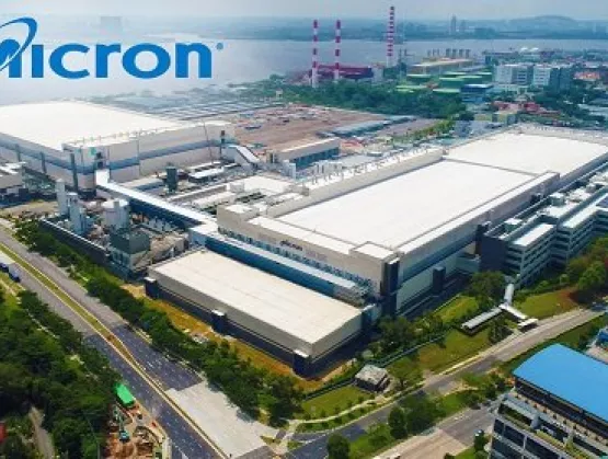
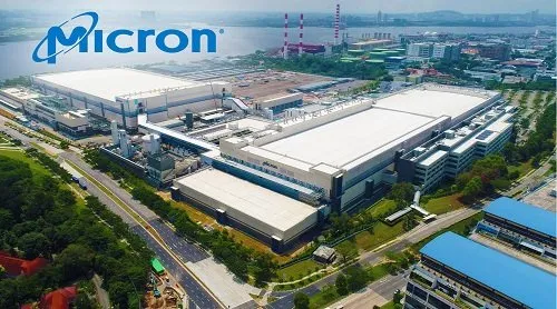
Making Strides TogetherKnowledge is power – especially when it is shared. This principle formed the foundation for Micron’s Go and See virtual visit of its Singapore manufacturing plant on 26 August 2020 as 27 companies including GLOBALFOUNDRIES, ST Microelectronics, Infineon, TEL, ViTrox , IBM, HP and UTAC joined the first-of-a-kind virtual factory visit. The chip industry powerhouses gathered to see how Micron’s Lighthouse frontend wafer fabrication facility leverages Fourth Industrial Revolution technologies to drive new production and cost efficiencies.They saw clear markers of a transformed organisation and spoke with working-level staff, managers and front-line employees. Company representatives also met virtually with Micron management teams from organisations that led its digital transformation – from pilot programs to integration at scale – to realise significant financial and operational benefits. The mix of technologies they deployed to make it all happen included artificial intelligence (AI), big data analytics and the Industrial Internet-of-Things (IIoT).Micron’s Singapore-based fab facility earned Lighthouse certification earlier this year from the World Economic Forum’s Global Lighthouse Network. The Go and See tour was co-sponsored by SEMI Southeast Asia and McKinsey Company.Transformation is CrucialBy embracing Lighthouse principles, semiconductor sectors and companies can accelerate their digital transformation to boost operational and financial efficiency while helping increase productivity across the electronics supply chain. It will take time for Southeast Asia semiconductor manufacturers to transform to digital operations, though we’re seeing growing interest in Industry 4.0 practices as they begin to understand that the deployment of new technologies and applications will help them better understand real-world benefits of smart manufacturing use cases and solutions. SEMI believes shining the spotlight on companies like Micron can illuminate the way forward for other companies to help drive the industry’s digital transformation. We look forward to seeing companies build on this momentum as they start to leverage leading-edge technologies to improve efficiencies and promote sustainability.Bee Bee Ng is president of SEMI Southeast Asia.
Read More
MEMS and image sensors are shining stars in the chip industry as technology companies worldwide accelerate innovation in the fight against COVID-19. The tiny devices are behind advances in areas of electronics ranging from thermal imaging and faster point-of-care testing to microfluidics-based polymerase chain reaction (PCR) tools and techniques to detect SARS-CoV-2.SEMI recently spoke with Yole Développement analysts Dimitrios Damianos and Chenmeijing Liang about MEMS and imaging sensors market trends and how microelectronics-enhanced technologies are supporting the worldwide push to contain the spread of COVID-19.For additional insights on the technologies, join the SEMI MEMS Imaging Sensors Summit, held for the first time at SEMICON Europa, 12-13 November 2020 in Munich, Germany. Registration is open.SEMI: Despite the global pandemic, the MEMS and sensors market is still growing and is one of the healthiest industries, not only in Europe, but globally. What is driving this growth?Damianos: MEMS have been continuously evolving from the first sensors that were measuring pressure and acceleration to rotation sensing and visible light management followed by light sensing beyond visible and the expansion to ultrasound and multi-spectral. Now we are heading towards an era where we want to sense every aspect of our environment, with more processing and eventually analytics bringing more quality to the data.COVID-19 has impacted various global markets in very different ways. While automotive, mobility and civil aviation have suffered, the impact on telecommunications and medical has been positive. The effects on the consumer, mobile and industrial markets have been moderate. Moreover, COVID-19 is changing the perception of the current global supply chain in manufacturing, potentially leading to more localized value chains and further regionalization in order to minimize similar risks posed by the pandemic and the first lockdown.SEMI: Who are the main MEMS players based on your research? Damianos: For MEMS players, the picture in 2019 was not the same as 10 years ago, when Texas Instruments (TI) and Hewlett-Packard (HP) were leading the scene, with Bosch and ST Microelectronics following, all at comparable revenue levels. Now, Broadcom and Bosch lead with almost $1.4 billion in revenue each, and the rest of the MEMS key stakeholders compete in the $400 million to $600 million league. Microphone players profited from the voice interface adoption trend, while players active in MEMS for mobility and smartphones suffered slightly due to weak end-system demand.SEMI: What scenarios can we expect for each market with regard to the impact of COVID-19 on MEMS for 2020? Damianos: For 2020, at Yole Développement we expect the consumer market to contract slightly by 2.6%, with the automotive market to dip by 27.5%, and defense and aerospace by 20.5%. For the defense market, no major effect is expected, as all major programs still run for the year. The market may experience some slight delays in deliveries due to supply chain and logistics problems. However, sensors integrated in commercial/civil aerospace applications will suffer due to the general paralysis of the air travel industry. On the positive side, telecommunications could increase by 4.7%, medical applications by 10.6%, and industrial by 11.5%.Due to the global pandemic, some types of MEMS have spiked in demand this year. For example, demand for thermopiles and microbolometers used in temperature guns and thermal cameras has increased because of the need for contactless monitoring of people’s temperatures. Moreover, microfluidics for DNA sequencing and real-time polymerase chain reaction (PCR) diagnostic tests for detecting COVID-19 are gaining market relevance, with the latter serving as a premier method of detecting a bacteria or virus on the molecular level with high degrees of accuracy. Furthermore, pressure and flowmeters in ventilators will grow because of huge demand by hospital intensive care units (ICUs).SEMI: What growth trends do you predict for the long haul?Damianos: In the longer term, we expect global MEMS volumes to almost double, from 24.4 billion units in 2019 to 50.8 billion units in 2025, with a 13% CAGR during the same period. The global MEMS market could reach $17.7 billion in revenue by 2025.We see a trend to more wearable devices integrating a lot of sensors but also a move to a more consumer-oriented healthcare. Moreover, everything related to voice interfaces and voice/virtual-personal assistants (VPAs) will continue to see strong growth, increasing demand for MEMS mics with better quality and high-fidelity voice capture. MEMS devices are shifting to higher accuracy, ultra-low power, embedded intelligence and possibly some bio-compatibility for medical applications.MEMS players will try to escape the commoditization cycle and deliver more value by increasing the value of the data, either grouping many sensors to create sensor hubs or by adding processing, algorithms and software. Industry players are employing strategies such as adding extra processing close to the sensor (e.g. Knowles) or ameliorating the use cases of their applications of their clients (e.g. Bosch or ST). AI on the edge seems very alluring for extra value acquisition, with many startups already working on it. Some examples include always-on-sensing (Aspinity in collaboration with Infineon, Syntiant), echolocation (IMERAI) and predictive maintenance using inertial sensors (Cartesiam). This will be the next pit stop for MEMS technology for sure. SEMI: The CMOS Image Sensor (CIS) is a cornerstone technology in the development of devices powered by machine sensing and artificial intelligence (AI) for applications such as advanced driver assistance system (ADAS). CIS powers many of the ongoing revolutions in new technical products and use cases. What is the status of the image sensors industry? Liang: Last year was exceptional with a combination of high demand and high prices due to capacity limitations. Q4 2019 went way above the forecast, and, in the end, the CIS industry reached $19.3 billion for the full year. This year, we think it will return to normal, and, despite the pandemic impact, we expect significant growth in the range of 7% to 12%. Last year’s 25% year-over-year (YOY) growth was the highest we’ve seen over the past decade. Mobile still dominates the marketplace for CIS with 69% market share. Two markets, computing (8%) and consumer (5%), are adjacent to the mobile market but progressively losing ground due to the smartphone disruption.Security, at 6% market share, will probably be the second largest CIS market in the future. Although this is an area of excellence for the emerging Chinese players, unfortunately, they could be hit by the current trade war. The automotive market did very well from 2018 to 2019 because of the numerous applications recently developed for ADAS, viewing, and in-cabin applications. Lastly, the industrial camera applications benefited from large investments in automation, especially in the semiconductor and automotive industries, but here again many uncertainties remain as these markets will reshuffle in the post COVID-19 world. SEMI: Which CIS markets are most susceptible to seasonality and the impact of COVID-19?Liang: According to our quarterly CIS monitor, automotive and security were both negatively impacted by the pandemic beyond what we expected in terms of seasonality. For computing, the situation improved just prior the lockdown. Q1 got a positive impact with high sales results for laptops and tablets, but no significant impact was seen for security equipment. For automotive, the demand for cameras was very high in Q1, which is seasonally normal, despite the decrease of car shipments that followed later. The automotive CIS market in 2020 should remain relatively flat compared to 2019 due to the higher attachment rates of cameras despite the lower number of cars produced. Consumer and industrial segments dropped in Q1, which is typical early in the year.The next five years might be a bit slow, and although we forecast growth for the next year, in the future the market share will be lower in mobile. In fact, mobile CIS growth will fall below the CIS growth average, but we will see an increase of market share for the security, automotive and industrial segments. The CIS market could reach $28 billion in 2025.At first, COVID-19 had a limited impact on the production side, as factories in China are usually closed for the New Year holiday, when the pandemic started. While supply is currently recovering, we still consider the limited impact on demand. Smartphone production for 2020 will be down 6%, but camera shipments for mobile should increase about 10% this year. Another positive trend for the mobile market is optical fingerprint implementation. Currently, high-end Android phones use this kind of technology. For 2023, we estimate optical fingerprint technology revenue to be over $1 billion.The roadmap for the automotive market is driven by camera proliferation. We’ll see 10 cameras per car and more for some high-end vehicles. Increasing demand for safety and convenience will mean more cameras per car in the future. With a strong attachment rate, the market average in automotive is around 2.0 cameras per car nowadays, and we expect the market average to reach 3.5 cameras per car in 2025. In security, Charge Coupled Device (CCD)-based cameras are nearly out of the market, as CMOS-based IP cameras are most important now.SEMI: What are current key technology trends?Liang: 3D semiconductor technology is the hot topic. CIS wafer staking technology is indeed at the center of the CIS technology race. Future applications could be AI analytics or recently developed applications on new types of CIS. So far, we have seen the introduction of variants of the CIS pixel. Global shutter (GS) and indirect Time of Flight (iToF) were recently introduced, and now direct time-of-flight (dTOF) pixels are being used in high volume. 3D semiconductor technology is a bonanza for the industry, as it allows to pack more value in a single chip. While the surface of silicon is still increasing, additional silicon is added through stacking.With COVID-19 still a problem, the endpoint for smartphones in 2020 remains uncertain. The short-term impact for CIS will be slower growth with respect to the 25% YoY of last year. The downturn in car production will be mitigated by an increased attachment rate for automotive cameras. The security market will also help maintain CIS growth.For more insights, see the following reports: Status of the MEMS Industry 2020 3D Imaging and Sensing 2020 CIS Market Monitor Q2 2020 Dimitrios Damianos is a technology and market analysts at Yole Développement covering MEMS, Sensors, Photonics and Imaging. Chenmeijing Liang is a technology and market analysts at Yole Développement covering Imaging. Serena Brischetto is senior manager of Marketing and Communications at SEMI Europe.
Read More
Japan’s semiconductor industry has weathered the COVID-19 pandemic to post robust growth. Far from a temporary setback, COVID-19 will lead to enduring change in how we work and live. And just as automation has been a bulwark against the devastating business impacts of the virus outbreak, increasing digitization will lead to new efficiencies in our industry.These were some of the key takeaways from three SEMI Japan Members Day webinars in June and July that offered the latest updates on COVID-19 impacts to the semiconductor industry and restart strategies for SEMI members. More than 2,000 SEMI members across Japan’s islands attended the webinars featuring the following five speakers: Hideki Kanewaka, Marketing Director, Consulting Lead, Japan, Accenture Japan Ltd. Takayuki Komori, Manager, Marketing Engineering Dept, SUMCO Corporation Taketoshi Hamaguchi, Director, Manufacturing Industry, Microsoft Corporation Akira Minamikawa, Senior Consulting Director, OMDIA (Informa Intelligence LCC) Yuichi Koshiba, Managing Director Partner, Boston Consulting Group COVID-19 Impact on Japan Semiconductor Industry is ModestThe consensus view of the five speakers from various quarters of the industry – consultant, IT service provider, materials supplier, market analyst – was that the Japan semiconductor industry withstood the heavy blows COVID-19 dealt to other industries thanks to strong demand for chips. Shelter-in-place policies and lockdowns spawned by COVID-19 has accelerated the digital transformation rippling around the world as electronics sales have soared to support everything from remote work and education to healthcare and home entertainment including gaming.The rapid growth of cloud usage for video streaming, gaming and remote work is taxing communications network capacity and placing more bandwidth demands on servers, said Akira Minamikawa of OMDIA. According to a recent report by Nokia, communications network traffic has skyrocketed 300 percent for online meetings and 400 percent for gaming, bringing the networks closer to their capacity limits. Minamikawa sees server shipments increasing at 8 percent CAGR through 2024. For the broader chip market, he expects demand for notebooks, solid state and hard disk drives, and gaming to remain strong in 2020. He also predicts rapid 5G penetration for smartphones will boost semiconductor chip industry growth.Still, not all semiconductor segments are expanding, said Yuichi Koshiba of Boston Consulting Group. Chip shipments for end products in markets such as automotive, industrial equipment and aircrafts are on the decline. Slowing demand for chips that power automotive applications in particular could pare sales for some chip companies and distributors since the segment accounts for a high proportion of their overall revenue.State of the Semiconductor IndustryFrom SUMCO’s vantagepoint as a major silicon wafer supplier, the company’s Takayuki Komori sees a number of changes unfolding in the semiconductor industry: Smartphones are driving growing demand for process technology (smaller nodes) and 300mm wafers. Komori estimates the typical high-end smartphone sports 1,700 square millimeters of silicon. 300mm wafers account for 80 percent of that total while more than 50 percent of the devices use leading edge multi-patterning technologies. Smartphones will need more RF chips to support 5G’s high-speed communications and added frequency ranges. Substrates for RF switches and tuners have been shifting from gallium arsenide (GaAs) and other compound semiconductors to silicon. 5G smartphone penetration will accelerate as the cost of integrating CPUs and modem functions into a single chip sees a swift decline. While the sensitivity and resolution of CMOS image sensors have evolved to incorporate innovative backside illumination and stacking technologies, future advances will focus more on products for machine vision applications capable of sensing invisible light bands. Rising adoption of electric vehicles and robotics applications will drive growing demand for power semiconductors that control their motors such as IGBTs and MOSFETs as the production capacity for the devices expands and shifts to 300mm wafer lines. For memory fabs, Minamikawa said utilization remains high as a result of a spending slowdown by major chip manufacturers and will stay elevated even once additional capacity ramps to support robust demand. Foundry fab utilization also remains high despite the pandemic-driven cancellation of smartphone chip orders in March. Minamikawa also sees the utilization rate of micro rising with the surge in demand for notebooks, PCs and servers in the second half of 2020.Transition to New NormalAs people around the world start to settle into new ways of living and working, there’s a growing acceptance that the transformation will be long-lasting. And no area of people’s lives is changing more than their work. Boosted by government subsidies, many small and midsize companies in Japan have started to implement work-from-home policies, an area where major electronics and IT businesses had already instituted reforms, said Hideki Kanewaka of Accenture. A few examples: Nippon Telegraph and Telephone Corporation (NTT) announced that half of its employees will continue to work from home in the future. A five-year plan Toshiba launched in 2019 to allow all employees to work from home will likely accelerate. Hitachi plans to allow all employees to work from home starting in April 2021. dwango, a major internet-based entertainment company in Japan, announced it will allow in principle any employees to work remotely. In the critical area of remote sales, Kanewaka pointed to the importance of going beyond online business meetings, paperless transactions and virtual events to devise new ways to attract customers and close deals. Creating online communities and providing rich digital content are also important measures to consider, he said.Manufacturing's Digital TransformationTravel restrictions by most countries to curb the COVID-19 outbreak have also raised barriers to chip companies sending engineers overseas sites to service state-of-art equipment and provide other technical support. Microsoft’s remote assist system deployed by ASML is one tool semiconductor makers can use to overcome this challenge, said Taketoshi Hamaguchi of Microsoft.The system connects a remote equipment service expert with an onsite worker through the internet, allowing the technical expert to provide support through a goggle display with a camera worn by the worker. Guided by the expert, the worker can perform complex services. A Natural User Interface (NUI) helps give the factory worker a clear understanding of the often highly technical instructions.Using artificial intelligence (AI) to increase automation will also help reduce the reliance of semiconductor factories on onsite workers. For example, AI deep learning can be deployed to calibrate equipment autonomously and reduce downtime after scheduled maintenances, Hamaguchi said.Corporate Restart Strategies Beyond factory considerations tied to COVID-19, semiconductor companies will need to adapt their business strategies to new ways of operating. For example, global supply chains will shift to domestic sources and increase redundancy to ensure a steady supply, a change leading to higher overall costs, Koshiba said. Trade routes among regions will also be redrawn as the trade rift between the United States and China and other geopolitical tensions intensify. The total value of those routes is expected to recover by 2023.Koshiba advised companies to evaluate the supply chain trade-offs between stability and cost and factor in potential risks to improve their short-term resilience and drive mid- to long-term supply chain restructuring.After past recessions, 14 percent of companies restored sales growth, Koshiba said. He recommended investing aggressively in growth and seizing M A opportunities during the downturn. Chip companies must also adapt to supply chain changes faster than competitors.Become a SEMI MemberWebinars like the recent SEMI Japan Members Day series have become increasingly important in the mix of programs and services SEMI offers members to help them connect, collaborate and innovate in the microelectronics community. To become a SEMI member, please visit the SEMI website or contact your nearest SEMI office.Jim Hamajima is president of SEMI Japan.
Read More